Yealink YL43455 Bluetooth and FM Receiver Combo Stamp Module
YL43455 IEEE 802.11a/b/g/n/ac Wireless LAN, Bluetooth and FM receiver Combo Stamp Module
General Description
The YL43455 IEEE 802.11 a/b/g/n/ac SDIO Wi-Fi with Bluetooth and FM receiver combo stamp module is a highly integrated wireless local area network (WLAN) solution to let users enjoy the digital content through the latest wireless technology without using the extra cables and cords. It combines with Bluetooth and provides a complete 2.4GHz Bluetooth system that is fully compliant to Bluetooth and SDIO v3.0 that supports EDR of 2Mbps and 3Mbps for data and audio communications. It enables a high-performance, cost-effective, low-power, compact solution that easily fits onto the SDIO and UART stamp module.
Compliant with the IEEE 802.11a/b/g/n/ac standard, YL43455 uses Direct Sequence Spread Spectrum (DSSS), Orthogonal Frequency Division Multiplexing (OFDM), BPSK, QPSK, CCK and QAM baseband modulation technologies.
A high level of integration and full implementation of the power management functions specified in the IEEE 802.11 standard minimize system power requirements by using YL43455.
YL43455 module adopts BCM43455 single chip solution. The module design is based on the BCM43455 solution.
Key Features
- 1. High-speed wireless connection up to 433.3Mbps for Wi-Fi
- 1(Transmit) 1(Receive) Wi-Fi and Bluetooth
- Low power consumption and high performance
- Enhanced wireless security
- Fully qualified Bluetooth
- Enhanced Data Rate(EDR) compliant for both 2Mbps and 3Mbps supported
Specifications Table
| Model Name | YL43455 |
| Description | Wireless LAN &Bluetooth Stamp Module |
| WLAN Standard | IEEE 802.11 a/b/g/n/ac |
| Bluetooth Standard | Bluetooth 2.1+Enhanced Data Rate (EDR)+ BLE(1M) |
| Major Chipset | BCM43455 |
| Host Interface | Wi-Fi : SDIO, BT :UART |
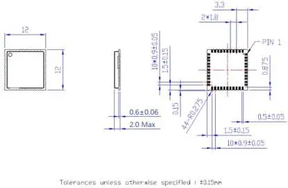
| Dimensions | 12mm * 12mm * 2.0mm |
| Operating Conditions | |
| Voltage | power supply for host:3.3V |
| Temperature | -40℃~85℃ |
| Storage temperature | -45℃~135℃ |
| Electrical Specifications | |
|
Frequency Range | WLAN: 2.4 GHz ISM Bands 2.412-2.462 GHz 5G:5.150~5.250GHz, 5.250~5.350GHz, 5.47~5.725GHz 5.725~5.85GHz Bluetooth: 2402~2480MHz |
|
Modulation | DSSS, OFDM, DBPSK, DQPSK, CCK, 16-QAM, 64-QAM,256-QAM for WLAN GFSK (1Mbps), Π/4 DQPSK (2Mbps) and 8DPSK (3Mbps) for Bluetooth |
|
Output Power | WLAN: 2412-2462MHz: 15.55dBm 5150-5250MHz: 14.12dBm 5250-5350MHz: 14.38dBm 5470-5725MHz: 12.04dBm 5725-5850MHz: 13.37dBm BT: 2402-2480MHz: 7.74dBm |
|
Data Rates | WLAN 802.11b: 1, 2, 5.5, 11Mbps 802.11a/g: 6, 9, 12, 18, 24, 36, 48, 54Mbps 802.11n: up to 75Mbps-single 802.11n: up to 150Mbps 802.11ac:up to 96Mbps (20MHz channel) 802.11ac:up to 200Mbps (40MHz channel) 802.11ac:up to 433Mbps (80MHz channel) Bluetooth Bluetooth 2.1+EDR data rates of 1,2, and 3Mbps |
|
Security | u WAPI u WEP 64-bit and 128-bit encryption with H/W TKIP processing u WPA/WPA2(Wi-Fi Protected Access) u WMM/WMM-SA/WMM-PS (U-APSD) u AES-CCMP hardware implementation as part of 802.11i security |
| standard | |
| Operating System Compatibility | TBD |
Electrical Characteristics
Absolute Maximum Ratings
| Symbol | Parameter | Maximum | Unit |
| VBAT | 3.3V power supply voltage | 5.25 | V |
| VDDIO | Voltage supply for GPIO | 3.9 | V |
| RFin | Maximum RF input (reference to 50 Ω) | TBD | dBm |
Recommended Operating Conditions
| Symbol | Parameter | Rating | Unit |
| VDD | 3.3V power supply voltage | 3.2~4.8 | V |
| VDDIO | Voltage supply for GPIO | 1.62~3.63 | V |
GPIO DC Characteristics
| Symbol | Parameter | Minimum | Typical | Maximum | Unit |
| VIH | Input high voltage | 0.65×VDDIO | — | VIO+0.3 | V |
| VIL | Input low voltage | — | — | 0.35×VIO | V |
| VOH | Output high voltage | VIO-0.45 | — | VIO | V |
| VOL | Output low voltage | 0 | — | 0.45 | V |
Pin Definition
Pin Description 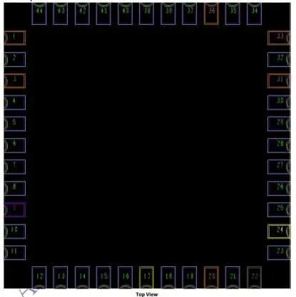
| Pin No. | Definition | Basic Description Type | Type |
| 1 | GND | GROUND | GND |
| 2 | WL_BT_ANT | Wi-Fi/BT RF signal | I/O |
| 3 | GND | GROUND | GND |
| 4 | NC | Floating Pin, No connect to anything. | Floating |
| 5 | NC | Floating Pin, No connect to anything. | Floating |
| 6 | Host_Wakeup_BT/GPIO34 | Host wakeup BT device | IN |
| 7 | BT_wakeup_Host | BT Device wakeup Host | I/O |
| 8 | TMS | Reserve for EJTAG | I/O |
| 9 | VDD | DC power supply +3.3V input | VCC |
| 10 | NC | Floating Pin, No connect to anything. | Floating |
| 11 | NC | Floating Pin, No connect to anything. | Floating |
| 12 | WL_EN | GPIO pin to on/off the Wi-Fi function by software. Active high. Reserve pull high | IN |
| 100K resistor and shunt 100pF capacitor to GND on platform. | |||
| 13 | WL_wakeup_Host/GPIO35 | WLAN device wakeup host | OUT |
| 14 | SDIO_DATA2 | SDIO Data Line 2 | I/O |
| 15 | SDIO_DATA3 | SDIO Data Line 3 | I/O |
| 16 | SDIO_CMD | SDIO Command Input | I/O |
| 17 | SDIO_CLK | SDIO Clock Input | IN |
| 18 | SDIO_DATA0 | SDIO Data Line 0 | I/O |
| 19 | SDIO_DATA1 | SDIO Data Line 1 | I/O |
| 20 | GND | GROUND | GND |
| 21 | CLK_REQ/GPIO11 | Clock request output | DO |
| 22 | VDDIO | 1.8V-3.3V VDDIO supply for WLAN and BT | VCC |
| 23 | NC | Floating Pin, No connect to anything. | Floating |
| 24 | LPO | External low-power 32.768KHz clock input. | IN |
| 25 | PCM_OUT | PCM synchronous data output, connected to PCM_IN on the host. | OUT |
| 26 | PCM_CLK | PCM Clock | I/O |
| 27 | PCM_IN | PCM synchronous data input, connected to PCM_OUT on the host. | IN |
| 28 | PCM_SYNC | PCM synchronous data SYNC | I/O |
| 29 | TDI | Reserve for EJTAG | IN |
| 30 | TDO | Reserve for EJTAG | OUT |
| 31 | GND | GROUND | GND |
| 32 | TCK | Reserve for EJTAG | GND |
| 33 | GND | GROUND | GND |
|
34 |
BT_EN | GPIO pin to on/off the BT function by software. Active high. Reserve pull high 100K resistor and shunt 100pF capacitor to GND on host. |
IN |
| 35 | NC | Floating Pin, No connect to anything. | Floating |
| 36 | GND | GROUND | GND |
| 37 | NC | Floating Pin, No connect to anything. | Floating |
| 38 | NC | Floating Pin, No connect to anything. | Floating |
| 39 | Debug_UART_TXD | TXD for Wi-Fi Uart_debug only, connected to RXD of the host. | OUT |
| 40 | Debug_UART_RXD | RXD for Wi-Fi Uart_debug only, connected to TXD of the host. | IN |
| 41 | UART_RTS | UART Ready To Send, connected to CTS on the host. | OUT |
| 42 | UART_TXD | UART Transmit Data, connected to RXD on | OUT |
| the host. | |||
| 43 | UART_RXD | UART Receive Data, connected to TXD on the host. | IN |
| 44 | UART_CTS | UART Clear To Send, connected to RTS on the host. | IN |
Mechanical Information
FCC WARNING
This equipment has been tested and found to comply with the limits for a Class B digital device, pursuant to part 15 of the FCC Rules. These limits are designed to provide reasonable protection against harmful interference in a residential installation. This equipment generates uses and can radiate radio frequency energy and, if not installed and used in accordance with the instructions, may cause harmful interference to radio communications. However, there is no guarantee that interference will not occur in a particular installation. If this equipment does cause harmful interference to radio or television reception, which can be determined by turning the equipment off and on, the user is encouraged to try to correct the interference by one or more of the following measures:
- Reorient or relocate the receiving antenna.
- Increase the separation between the equipment and receiver.
- Connect the equipment into an outlet on a circuit different from that to which the receiver is connected.
- Consult the dealer or an experienced radio/TV technician for help.
Any Changes or modifications not expressly approved by the party responsible
for compliance could void the user’s authority to operate the equipment.
This device complies with part 15 of the FCC Rules. Operation is subject to the following two conditions: (1) This device may not cause harmful interference, and (2) this device must accept any interference received, including interference that may cause undesired operation.
FCC RF EXPOSURE STATEMENT:
This equipment complies with FCC radiation exposure limits set forth for an uncontrolled environment.
This transmitter must not be co-located or operating in conjunction with any
other antenna or transmitter.
This equipment should be installed and operated with minimum distance 20cm between the radiator& your body.
Integration instructions for host product manufacturers according to KDB 996369
D03 OEM
Manual v01
List of applicable FCC rules CFR 47 FCC PART 15 SUBPART C/E has been investigated. It is applicable to the modular.
Specific operational use conditions
This module is stand-alone modular. If the end product will involve the Multiple simultaneously transmitting condition or different operational conditions for a
the stand-alone modular transmitter in a host, host manufacturer have to consult with module manufacturer for the installation method in end system.
Limited module procedures
Not applicable
Trace antenna designs
Not applicable
RF exposure considerations
To maintain compliance with FCC’s RF exposure guidelines, this equipment should
be installed and operated with a minimum distance of 20cm from your body.
Antennas
This radio transmitter FCC ID: T2C-YL43455 has been approved by Federal Communications Commission to operate with the antenna types listed below, with the maximum permissible gain indicated. Antenna types not included in this list that have a gain greater than the maximum gain indicated for any type listed are strictly prohibited for use with this device.
| Antenna type | Maximum Antenna gain |
| PCB Antenna | 3dBi |
Label and compliance information
The final end product must be labeled in a visible area with the following
” Contains FCCID: T2C-YL43455”
Information on test modes and additional testing requirements
Host manufacturer is strongly recommended to confirm compliance with FCC requirements for the transmitter when the module is installed in the host.
Additional testing, Part 15 Subpart B disclaimer
Host manufacturer is responsible for compliance of the host system with module installed
with all other applicable requirements for the system such as Part 15 B


