Shenzhen ESP32-SL WIFI and BT Module User Manual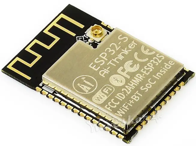
Disclaimer and copyright notice
The information in this article, including the URL for reference, is subject to change without notice.
The document is provided “as is” without any guarantee responsibility, including any guarantee of marketability, suitability for a specific purpose or non-infringement, and any guarantee mentioned elsewhere in any proposal, specification or sample. This document assumes no responsibility, including any liability for infringement of any patent rights arising from the use of the information in this document. This document does not grant any license to use intellectual property rights, whether express or implied, by estoppel or other means.The test data obtained in this article are all obtained by Enxin Lab’s laboratory tests, and the actual results may be slightly different.
The Wi-Fi Alliance member logo is owned by the Wi-Fi Alliance.
All trademark names, trademarks and registered trademarks mentioned in this articleare the property of their respective owners and are hereby declared.
The final interpretation right belongs to Shenzhen Anxinke Technology Co., Ltd
Attention
The contents of this manual may change due to product version upgrade or other reasons. Shenzhen Anxinke Technology Co., Ltd. reserves the right to modify the contents of this manual without any notice or prompt. This manual is only used as a guide. Shenzhen Anxinke Technology Co., Ltd. makes every effort to provide accurate information in this manual, but Shenzhen Anxinke Technology Co., Ltd. does not guarantee that the contents of the manual are completely error-free. And the suggestion does not constitute any express or implied guarantee.
Formulation/Revision/Abolition of CV
| Version | Date | Formulation/Revision | Maker | Verify |
| V1.0 | 2019.11.1 | First formulated | Yiji Xie | |
PRODUCT OVERVIEW
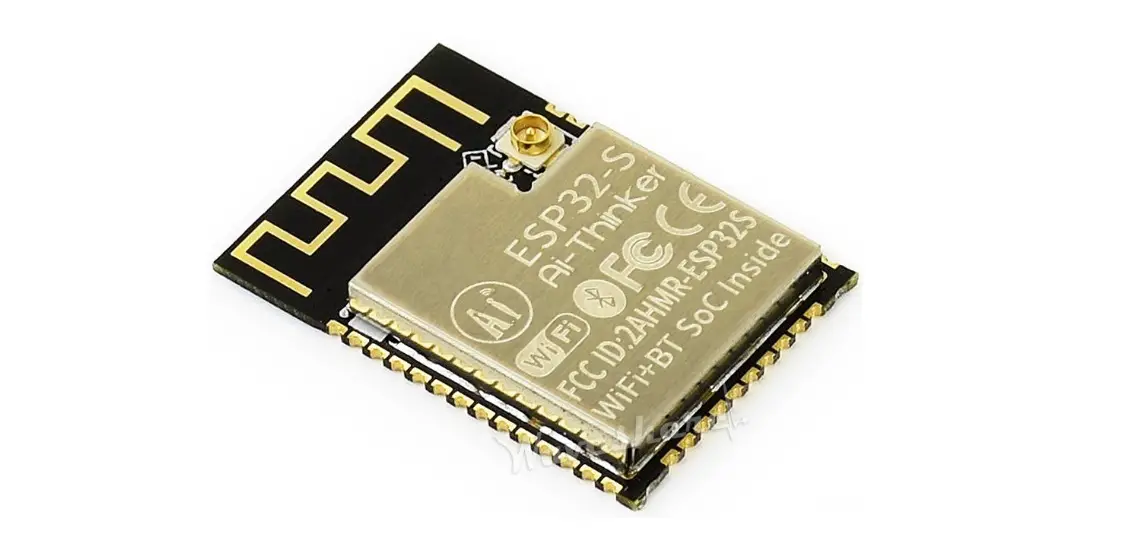
ESP32-SL is a general-purpose Wi-Fi+BT+BLE MCU module, with the industry’s most competitive package size and ultra-low energy consumption technology, the size is only 18*25.5*2.8mm.
ESP32-SL can be widely used in various IoT occasions, suitable for home automation, industrial wireless control, baby monitors, wearable electronic products, wireless position sensing devices, wireless positioning system signals, and other IoT applications. It is an IoT application Ideal solution.
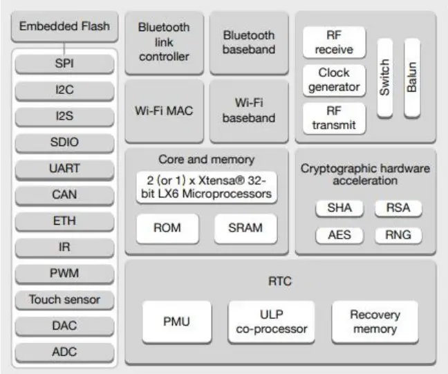
The core of this module is the ESP32-S0WD chip, which is scalable and adaptive. The user can cut off the power of the CPU and use the low power consumption to assist the processor to continuously monitor the status changes of peripherals or whether certain analog quantities exceed the threshold. ESP32-SL also integrates a wealth of peripherals, including capacitive touch sensors, Hall sensors, low-noise sensor amplifiers, SD card interface, Ethernet interface, high-speed SDIO/SPI, UART, I2S andI2C. The ESP32-SL module is developed by Encore Technology. The core processorESP32 of the module has a built-in low-power Xtensa®32-bit LX6 MCU, and the main frequency supports 80 MHz and 160 MHz.
ESP32-SL adopts SMD package, which can realize the rapid production of products through standard SMT equipment, providing customers with highly reliable connection methods, especially suitable for modern production methods of automation, large-scale,and low cost, and is convenient to apply to various IoT hardware Terminal occasions.
Characteristics
- Complete 802.11b/g/n Wi-Fi+BT+BLE SOC module
- Using low-power single-core 32-bit CPU, can be used as an application processor, the main frequency is up to 160MHz, the computing power is 200 MIPS, support RTOS
- Built-in 520 KB SRAM
- Support UART/SPI/SDIO/I2C/PWM/I2S/IR/ADC/DAC
- SMD-38 packaging
- Support Open OCD debug interface
- Support multiple sleep modes, the minimum sleep current is less than 5uA
- Embedded Lwip protocol stack and Free RTOS
- Support STA/AP/STA+AP work mode
- Smart Config (APP)/AirKiss (WeChat) one-click distribution network supporting Android and IOS
- Support serial local upgrade and remote firmware upgrade (FOTA)
- General AT command can be used quickly
- Support secondary development, integrated Windows, Linux development
environment
Major parameter
List 1 description of major parameter
| Model | ESP32-SL |
| Packaging | SMD-38 |
| Size | 18*25.5*2.8(±0.2)MM |
| Antenna | PCB antenna/external IPEX |
| Spectrum range | 2400 ~ 2483.5MHz |
| Work frequency | -40 ℃ ~ 85 ℃ |
| Store environment | -40 ℃ ~ 125 ℃ , < 90%RH |
| Power supply | Voltage 3.0V ~ 3.6V,current >500mA |
| Power consumption | Wi-Fi TX(13dBm~21dBm):160~260mA |
| BT TX:120mA | |
| Wi-Fi RX:80~90mA | |
| BT RX:80~90mA | |
| Modem-sleep:5~10mA | |
| Light-sleep:0.8mA | |
| Deep-sleep:20μA | |
| Hibernation:2.5μA | |
| Interface supported | UART/SPI/SDIO/I2C/PWM/I2S/IR/ADC/DAC |
| IO port quantity | 22 |
| Serial rate | Support 300 ~ 4608000 bps ,default 115200 bps |
| Bluetooth | Bluetooth BR/EDR and BLE 4.2 standard |
| Safety | WPA/WPA2/WPA2-Enterprise/WPS |
| SPI Flash | Default 32Mbit, maximum support128Mbit |
ELECTRONICS PARAMETER
Electronic characteristics
| Parameter | Condition | Min | Typical | Max | Unit | |
| Voltage | VDD | 3.0 | 3.3 | 3.6 | V | |
| I/O | VIL/VIH | – | -0.3/0.75VIO | – | 0.25VIO/3.6 | V |
| VOL/VOH | – | N/0.8VIO | – | 0.1VIO/N | V | |
| IMAX | – | – | – | 12 | mA | |
Wi-Fi RF Performance
| Description | Typical | Unit |
| Work frequency | 2400 – 2483.5 | MHz |
| Output power | ||
| In 11n mode,PA output power is | 13±2 | dBm |
| In 11g mode,PA output power is | 14±2 | dBm |
| In 11b mode,PA output power is | 17±2 | dBm |
| Receiving sensitivity | ||
| CCK, 1 Mbps | <=-98 | dBm |
| CCK, 11 Mbps | <=-89 | dBm |
| 6 Mbps (1/2 BPSK) | <=-93 | dBm |
| 54 Mbps (3/4 64-QAM) | <=-75 | dBm |
| HT20 (MCS7) | <=-73 | dBm |
BLE RF Performance
| Description | Min | Typical | Max | Unit |
| Sending characteristics | ||||
| Sending sensitivity | – | +7.5 | +10 | dBm |
| Receiving characteristics | ||||
| Receiving sensitivity | – | -98 | – | dBm |
DIMENSION
PIN DEFINITION
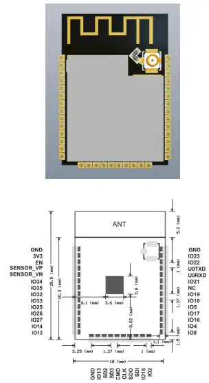
The ESP32-SL module has a total of 38 interfaces, as shown in the figure below. The following table shows the interface definitions.
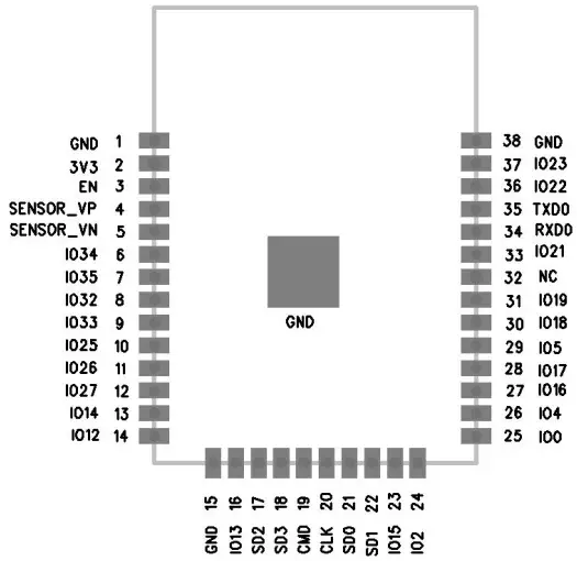
ESP32-SL PIN definition diagram
List PIN function description
| No. | Name | Function description |
| 1 | GND | Ground |
| 2 | 3V3 | Power supply |
| 3 | EN | Enable chip, high level is effective. |
| 4 | SENSOR_ VP | GPI36/ SENSOR_VP/ ADC_H/ADC1_CH0/RTC_GPIO0 |
| 5 | SENSOR_ VN | GPI39/SENSOR_VN/ADC1_CH3/ADC_H/ RTC_GPIO3 |
| 6 | IO34 | GPI34/ADC1_CH6/ RTC_GPIO4 |
| 7 | IO35 | GPI35/ADC1_CH7/RTC_GPIO5 |
| 8 | IO32 | GPIO32/XTAL_32K_P (32.768 kHz crystal oscillator input)/ ADC1_CH4/ TOUCH9/ RTC_GPIO9 |
| 9 | IO33 | GPIO33/XTAL_32K_N (32.768 kHz crystal oscillator output)/ADC1_CH5/TOUCH8/ RTC_GPIO8 |
| 10 | IO25 | GPIO25/DAC_1/ ADC2_CH8/ RTC_GPIO6/ EMAC_RXD0 |
| 11 | IO26 | GPIO26/ DAC_2/ADC2_CH9/RTC_GPIO7/EMAC_RXD1 |
| 12 | IO27 | GPIO27/ADC2_CH7/TOUCH7/RTC_GPIO17/ EMAC_RX_DV |
| 13 | IO14 | GPIO14/ADC2_CH6/ TOUCH6/ RTC_GPIO16/MTMS/HSPICLK /HS2_CLK/SD_CLK/EMAC_TXD2 |
| 14 | IO12 | GPIO12/ ADC2_CH5/TOUCH5/ RTC_GPIO15/ MTDI/ HSPIQ/ HS2_DATA2/SD_DATA2/EMAC_TXD3 |
| 15 | GND | Ground |
| 16 | IO13 | GPIO13/ ADC2_CH4/ TOUCH4/ RTC_GPIO14/ MTCK/ HSPID/ HS2_DATA3/ SD_DATA3/ EMAC_RX_ER |
| 17 | SHD/SD2 | GPIO9/SD_DATA2/ SPIHD/ HS1_DATA2/ U1RXD |
| 18 | SWP/SD3 | GPIO10/ SD_DATA3/ SPIWP/ HS1_DATA3/U1TXD |
| 19 | SCS/CMD | GPIO11/SD_CMD/ SPICS0/HS1_CMD/U1RTS |
| 20 | SCK/CLK | GPIO6/SD_CLK/SPICLK/HS1_CLK/U1CTS |
| 21 | SDO/SD0 | GPIO7/ SD_DATA0/ SPIQ/ HS1_DATA0/ U2RTS |
| 22 | SDI/SD1 | GPIO8/ SD_DATA1/ SPID/ HS1_DATA1/ U2CTS |
| 23 | IO15 | GPIO15/ADC2_CH3/ TOUCH3/ MTDO/ HSPICS0/ RTC_GPIO13/ HS2_CMD/SD_CMD/EMAC_RXD3 |
| 24 | IO2 | GPIO2/ ADC2_CH2/ TOUCH2/ RTC_GPIO12/ HSPIWP/ HS2_DATA0/ SD_DATA0 |
| 25 | IO0 | GPIO0/ ADC2_CH1/ TOUCH1/ RTC_GPIO11/ CLK_OUT1/ EMAC_TX_CLK |
| 26 | IO4 | GPIO4/ ADC2_CH0/ TOUCH0/ RTC_GPIO10/ HSPIHD/ HS2_DATA1/SD_DATA1/ EMAC_TX_ER |
| 27 | IO16 | GPIO16/ HS1_DATA4/ U2RXD/ EMAC_CLK_OUT |
| 28 | IO17 | GPIO17/ HS1_DATA5/U2TXD/EMAC_CLK_OUT_180 |
| 29 | IO5 | GPIO5/ VSPICS0/ HS1_DATA6/ EMAC_RX_CLK |
| 30 | IO18 | GPIO18/ VSPICLK/ HS1_DATA7 |
| 31 | IO19 | GPIO19/VSPIQ/U0CTS/ EMAC_TXD0 |
| 32 | NC | – |
| 33 | IO21 | GPIO21/VSPIHD/ EMAC_TX_EN |
| 34 | RXD0 | GPIO3/U0RXD/ CLK_OUT2 |
| 35 | TXD0 | GPIO1/ U0TXD/ CLK_OUT3/ EMAC_RXD2 |
| 36 | IO22 | GPIO22/ VSPIWP/ U0RTS/ EMAC_TXD1 |
| 37 | IO23 | GPIO23/ VSPID/ HS1_STROBE |
| 38 | GND | Ground |
Strapping PIN
| Built-in LDO(VDD_SDIO)Voltage | |||||||
| PIN | Default | 3.3V | 1.8V | ||||
| MTDI/GPIO12 | Pull down | 0 | 1 | ||||
| System startup mode | |||||||
| PIN | Default | SPI Flash startup mode | Download startup mode | ||||
| GPIO0 | Pull up | 1 | 0 | ||||
| GPIO2 | Pull down | Non-sense | 0 | ||||
| During system startup, U0TXD outputs log print information | |||||||
| PIN | Default | U0TXD Flip | U0TXD still | ||||
| MTDO/GPIO15 | Pull up | 1 | 0 | ||||
| SDIO slave signal input and output timing | |||||||
| PIN | Default | Falling edge output Falling edge input | Falling edge input Rising edge output | Rising edge input Falling edge output | Rising edge input Rising edge output | ||
| MTDO/GPI O15 | Pull up | 0 | 0 | 1 | 1 | ||
| GPIO5 | Pull up | 0 | 1 | 0 | 1 | ||
Note: ESP32 has 6 strapping pins in total, and the software can read the value of these 6 bits in the register “GPIO_STRAPPING”. During the chip power-on reset process, the strapping pins are sampled and stored in the latches. The latches are “0” or “1” and remain until the chip is powered off or turned off. Each strapping pin is
connected to internal pull-up/pull-down. If a strapping pin is not connected or the connected external line is in a high impedance state, the internal weak pull-up/pull-down will determine the default value of the strapping pin input level.
To change the value of the strapping bits, the user can apply external pull down/pull-up resistors, or apply the GPIOof the host MCU to control the level of the strapping pins at power-on reset of ESP32. After reset, the strapping pinhas the same function as the normal pin.
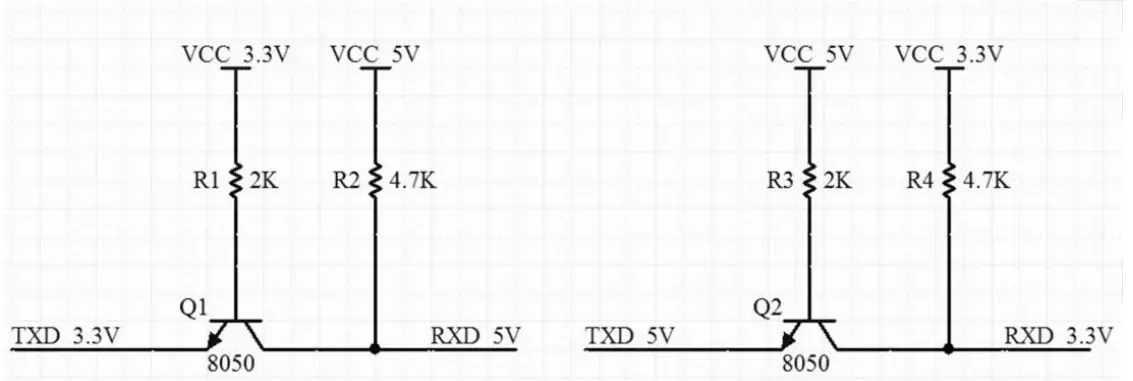
SCHEMATIC DIAGRAM
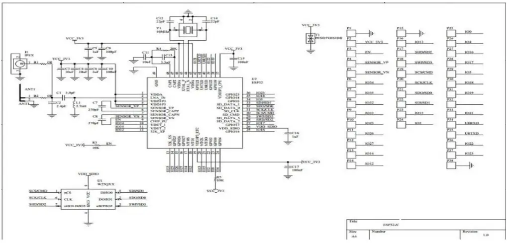
DESIGN GUIDE
Application circuit
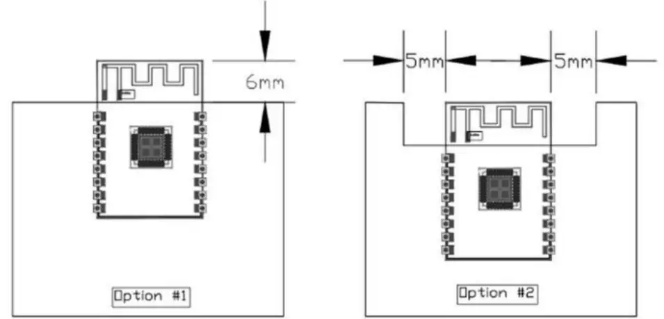
Antenna layout requirements
- The following two methods are recommended for the installation location on the motherboard:
Option 1: Place the module on the edge of the main board, and the antenna area protrudes from the edge of the main board.
Option 2: Place the module on the edge of the motherboard, and the edge of the motherboard digs out an area at the position of the antenna. - In order to meet the performance of the onboard antenna, it is forbidden to place metal parts around the antenna.

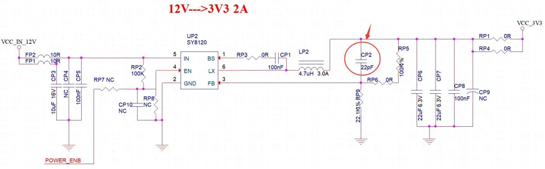
- Power supply
- 3.3V voltage is recommended, the peak current is more than 500mA
- It is recommended to use LDO for power supply; if using DC-DC, it is recommended to control the ripple within 30mV.
- It is recommended to reserve the position of the dynamic response capacitor in theDC-DC power supply circuit, which can optimize the output ripple when the load changes greatly.
- 3.3V power interface is recommended to add ESD devices.

- Use of GPIO port
- Some GPIO ports are led out of the periphery of the module. If you need to use a10-100 ohm resistor in series with the IO port is recommended. This can suppress overshoot, and the level on both sides is more stable. Help both EMI and ESD.
- For the up and down of the special IO port, please refer to the instruction manual of the specification, which will affect the startup configuration of the module.
- The IO port of the module is 3.3V. If the IO level of the main control and the module does not match, a level conversion circuit needs to be added.
- If the IO port is directly connected to the peripheral interface, or the pin header and other terminals, it is recommended to reserve ESD devices near the terminal of the IOtrace.

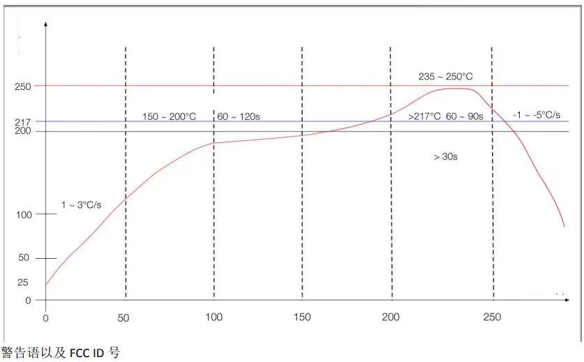
REFLOW SOLDERING CURVE
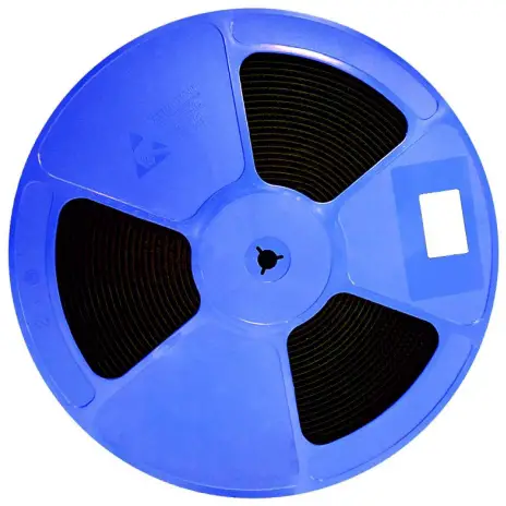
PACKAGING
As shown below, the packaging of ESP32-SL is taping.
CONTACT US
Web:https://www.ai-thinker.com
Development DOCS:https://docs.ai-thinker.com
Official forum:http://bbs.ai-thinker.com
Sample purchase:http://ai-thinker.en.alibaba.com
Business:[email protected]
Support:[email protected]
Add: 408-410, Block C, Huafeng Smart Innovation Port, Gushu 2nd Road, Xixiang, Baoan District,
Shenzhen
Tel:0755-29162996
Important Notice to OEM integrators
INTEGRATION INSTRUCTIONS
FCC rules
The ESP32-SL is an WIFI+BT Module Module with frequency hopping using an ASK modulation. It operates on the 2400 ~2500 MHz band and, therefore, is within U.S. FCC part 15.247 standard.
Modular installation instruction
- ESP32-SL Integrates high-speed GPIO and peripheral interface. Please pay attention to the installation direction (pin direction).
- Antenna could not be in no-load state when module is working. During debugging, it is suggested to add 50 ohms load to the antenna port to avoid damage or performance degradation of the module under long-time no-load condition.
- When the module needs to output 31dBm or more power, it needs a voltage supply of 5.0V or more to achieve the expected output power.
- When working at full load, it is recommended that the entire bottom surface of the module be attached to the housing or heat dissipation plate, and it is not recommended to conduct heat dissipation through air or screw column heat conduction.
- UART1 and UART2 are serial ports with the same priority. The port which receives commands returns information.
Trace antenna designs
Not Applicable
RF exposure considerations
To maintain compliance with FCC’s RF Exposure guidelines, This equipment should be installed and operated with minimum distance between 20cm the radiator your body: Use only the supplied antenna.
Antennas
The ESP32-SL is an UHF RFID Module beams signals and communicates with its antenna, which is Panel Antenna.
LABEL OF THE END PRODUCT
The final end product must be labeled in a visible area with the following:
Host must Contains FCC ID: 2ATPO-ESP32-SL. If the size of the end product is larger than 8x10cm, then the following FCC part 15.19 statement has to also be available on the label: This device complies with Part 15 of FCC rules. Operation is subject to the following two conditions:
- this device may not cause harmful interference and
- this device must accept any interference received, including interference that may cause undesired operation.
Information on test modes and additional testing requirements5
Data transfer module demo board can control the EUT work in RF test mode at specified test channel.
Additional testing, Part 15 Subpart B disclaimer
The module without unintentional-radiator digital circuit, so the module does not required an evaluation by FCC Part 15 Subpart B. The host should be evaluated by the FCC Subpart B.
ATTENTION
This device is intended only for OEM integrators under the following conditions:
- The antenna must be installed such that 20 cm is maintained between the antenna and users, and
- This device and its antenna(s) must not be co‐located with any other transmitters except in accordance with FCC multi‐transmitter product procedures. Referring to the multi‐transmitter policy, multiple transmitter(s) and module(s) can be operated simultaneously without C2P.
- For all products market in US, OEM has to limit the Operating Frequency: 2400 ~2500MHz by supplied firmware programming tool. OEM shall not supply any tool or info to the end‐user regarding to Regulatory Domain change.
USERS MANUAL OF THE END PRODUCT:
In the user manual of the end product, the end user has to be informed to keep at least 20cm separation with the antenna while this end product is installed and operated. The end user has to be informed that the FCC radio‐frequency exposure guidelines for an uncontrolled environment can be satisfied. The end user has to also be informed that any changes or modifications not expressly approved by the manufacturer could void the user’s authority to operate this equipment.
If the size of the end product is smaller than 8x10cm, then additional FCC part 15.19 statement is required to be available in the users manual: This device complies with Part 15 of FCC rules.
Operation is subject to the following two conditions:
- this device may not cause harmful interference and
- this device must accept any interference received, including interference that may cause undesired operation.
FCC WARNING
This device complies with part 15 of the FCC Rules. Operation is subject to the following two conditions:
Any changes or modifications not expressly approved by the party responsible for compliance could void the user’s authority to operate the equipment.
NOTE: This equipment has been tested and found to comply with the limits for a Class B digital device, pursuant to Part 15 of the FCC Rules. These limits are designed to provide reasonable protection against harmful interference in a residential installation. This equipment generate, uses and can radiate radio frequency energy and, if not installed and used in accordance with the instructions, may cause harmful interference to radio communications. However, there is no guarantee that interference will not occur in a particular installation.
If this equipment does cause harmful interference to radio or television reception, which can be determined by turning the equipment off and on, the user is encouraged to try to correct the interference by one or more of the following measures:
- Reorient or relocate the receiving antenna.
- Increase the separation between the equipment and receiver.
- Connect the equipment into an outlet on a circuit different from that to which the receiver is connected.
- Consult the dealer or an experienced radio/TV technician for help.


