![]()
BDE-BLEM401P
Bluetooth Low Energy Module (BT4.2)
BDE-BLEM401P BDE-BLEM401P-U
Key Features
- Bluetooth Dual Mode 4.2 compliant
- Low-power 2.4GHz Transceiver
- ARM968E Core Microprocessor integrated
- 160 KB programmable Flash for Program and 20 KB RAM for Data
- Program code read protection
- Operation voltage from 0.9 V to 3.6 V
- Clock
 16 MHz crystal reference clock64 MHz digital PLL clock32 kHz ring oscillatorExternal 32 kHz crystal oscillatorMCU can run with any clock source with internal frequency divider
 - Interface and peripheral unitsJTAG, SPI interfaceUARTMulti-channels PWM outputOn-chip 10 bit general ADC13 GPIO with multiplexed interface functionsTrue random number generator
- RF PerformanceTX Power: up to 4dBmRX Sensitivity: up to -96dBm
- Communication Range: 30 meters (LOS)
- Antenna:Integrated PCB antenna - 401PIPEX/U.FL connector for external antenna - 401P-U
- Size: 16.55mm x 10.8mm x 1.5mm (Without Shielding)
16.55mm x 10.88 mm x 2.3mm (With Shielding) - Power Consumption:Shutdown: 1uA (Wake up on External Events)Standby: 8.5uA (RTC Running and RAM/CPU Retention)RX Current: 5.1mATX Current @ -1dBm: 4.8mA
- BQB (DID: D049515), FCC ID: 2ABRUBDLEM401P, CE, RoHS compliant
Descriptions
BDE-BLEM401P is a Bluetooth 4.2 dual mode compliant module targeted at low power sensors and PC/Phone accessories.
BDE-BLEM401P highly integrates a high-performance RF transceiver, baseband, ARM9E core, programmable protocol and profile to support BLE application. The module also offers flexible hardware interfaces for the sensor application.
It enables ultra-low power connectivity and data transfer for the applications that are sensitive to power consumption, size and cost.
Block Diagram
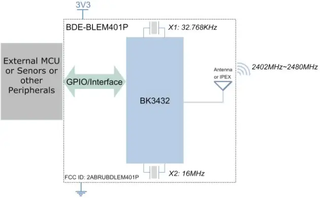 Fig. 1: The Block Diagram of BDE-BLEM401P
Applications
- Home and Building Automation
- Industrial
- Retail
- Health and Medical
- Sports and Fitness
- HID
Electrical Characteristics
- Recommended operating conditions
Rating | Min | Typ | Max | Unit |
| Operating Temperature | -40 | – | 85 | ℃ |
VDDS | 1.6 | 3.3 | 3.6 | V |
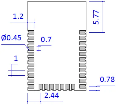
Pin Out
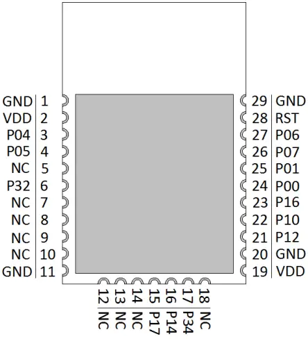 Fig. 2: The pinout of BDE-BLEM401P (TOP VIEW)
Table 1: Pin definitions of BDE- BLEM203P
| Pin Number | Pin Name | Definitions |
| 1 | GND | Power Ground |
| 2 | VDD | Power Supply |
| 3 | P04 | GPIO, SPI_SCK, SPI_MOSI (Program mode), JTAG_TDI (JTAG mode) |
| 4 | P05 | GPIO, SPI_MOSI, SPI_MISO (Program mode), JTAG_TDO (JTAG mode) |
| 5 | NC | NC |
| 6 | P32 | GPIO, ADC CH2 |
| 7 | NC | NC |
| 8 | NC | NC |
| 9 | NC | NC |
| 10 | NC | NC |
| 11 | GND | Power Ground |
| 12 | NC | NC |
| 13 | NC | NC |
| 14 | NC | NC |
| 15 | P17 | GPIO, UART2_RX |
| 16 | P14 | GPIO, PWM |
| 17 | P34 | GPIO, ADC CH4 |
| 18 | NC | NC |
| 19 | VDD | Power Supply |
| 20 | GND | Power Ground |
| 21 | P12 | GPIO, PWM |
| 22 | P10 | GPIO, PWM (20mA) |
| 23 | P16 | GPIO, UART2_TX |
| 24 | P00 | GPIO, UART_TX |
| 25 | P01 | GPIO, UART_RX |
| 26 | P07 | GPIO, SPI_NSS, SPI_CS (Program mode), JTAG_TMS (JTAG mode) |
| 27 | P06 | GPIO, SPI_MISO, SPI_SCK (Program mode), JTAG_TCK (JTAG mode) |
| 28 | RST | Reset, active low |
| 29 | GND | Power Ground |
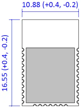
Overall Dimensions
Fig. 1 shows the overall dimensions of BDE-BLEM401P. The module measures 16.55mm long by 10.88mm wide by 2.3mm high with the shield.
 |  | 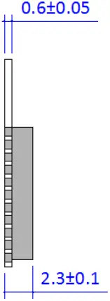 |
Top View | Bottom View | Side View |
Fig. 3: Overall Dimensions of BDE-BLEM401P
Module Location for Reference
In order to get a fine performance when integrate the module to your product, it is advised to use the recommended module location to the respective PCB.
- Location in X-Y plane
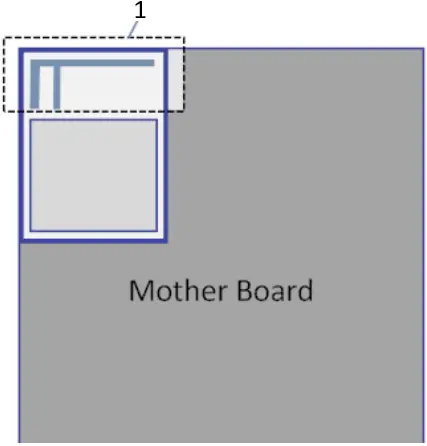
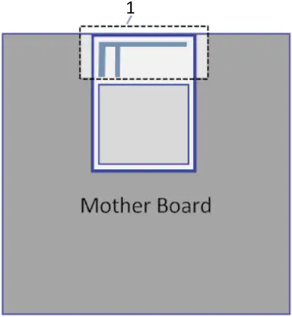
Fig. 4: Recommended location in X-Y plane
- Antenna area.
This area of the mother board should be cut off or copper free.
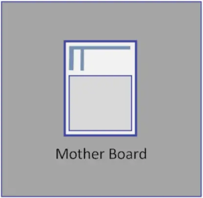
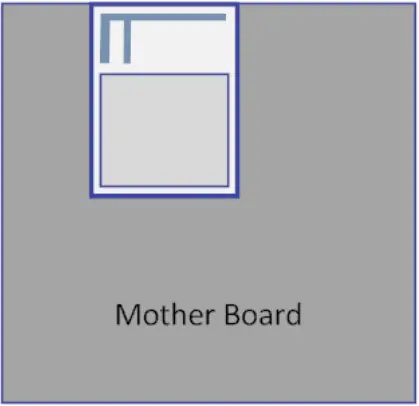
Fig. 5: Not recommended location in X-Y plane
- Location in Z plane
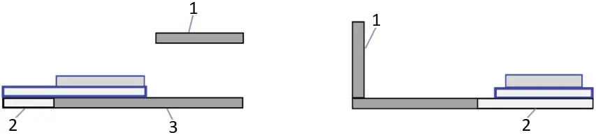 Fig. 6: Recommended location in Z plane
- Metal
- Cut off or copper free
- Mother Board
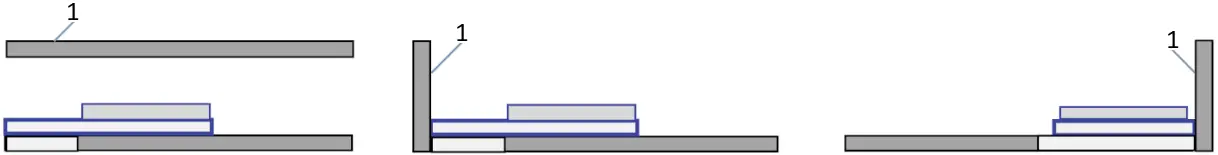 Fig. 7: Not recommended location in Z plane
- Metal
Typical Solder Reflow Profile
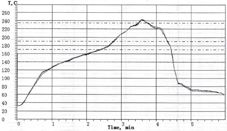 Fig. 8: Typical Solder Reflow Profile
Package Information
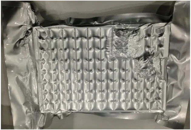 Fig. 9: Package
FCC statements
This device complies with part 15 of the FCC rules. Operation is subject to the following two conditions:
(1) This device may not cause harmful interference, and
(2) This device must accept any interference received, including interference that may cause undesired operation.
NOTE: The manufacturer is not responsible for any radio or TV interference caused by unauthorized modifications or changes to this equipment. Such modifications or changes could void the user’s authority to operate the equipment.
NOTE: This equipment has been tested and found to comply with the limits for a Class B digital device, pursuant to part 15 of the FCC Rules. These limits are designed to provide reasonable protection against harmful interference in a residential installation. This equipment generates uses and can radiate radio frequency energy and, if not installed and used in accordance with the instructions, may cause harmful interference to radio communications. However, there is no guarantee that interference will not occur in a particular installation. If this equipment does cause harmful interference to radio or television reception, which can be determined by turning the equipment off and on, the user is encouraged to try to correct the interference by one or more of the following measures:
– Reorient or relocate the receiving antenna.
– Increase the separation between the equipment and receiver.
– Connect the equipment into an outlet on a circuit different from that to which the receiver is connected.
– Consult the dealer or an experienced radio/TV technician for help.
The SAR limit of USA (FCC) is 1.6 W/kg averaged over one gram of tissue. Device types Panasonic ELUGA Ray 600 (FCC ID: 2APTIS60ER6) has also been tested against this SAR limit.The highest SAR value reported under this standard during product certification for use when properly worn on the body is 0.681 W/kg and for head is 0.898 W/kg. Simultaneous RF exposure is 1.233W/Kg. This device was tested for typical body-worn operations with the back of the handset kept 10mm from the body. To maintain compliance with FCC RF exposure requirements, use accessories that maintain a 10mm separation distance between the user’s body and the back of the handset. The use of belt clips, holsters and similar accessories should not contain metallic components in its assembly. The use of accessories that do not satisfy these requirements may not comply with FCC RF exposure requirements, and should be avoided.
Contacts
Guangzhou BDE Technology Inc.
Address: Originality Building B2-403, 162 Science Ave, Huangpu District, Guangzhou, 510663, China 494 E Thornhill Ln, Palatine, IL 60074, USA
Tel: +86-020-28065335 Fax: +86-020-28065338
Website: www.bdecomm.com Email: [email protected]
Guangzhou BDE Technology Inc.


