
kontron FlexATX-KBL-S-C236
Disclaimer
Kontron would like to point out that the information contained in this manual may be subject to alteration, particularly as a result of the constant upgrading of Kontron products. This document does not entail any guarantee on the part of Kontron with respect to technical processes described in the manual or any product characteristics set out in the manual. Kontron assumes no responsibility or liability for the use of the described product(s), conveys no license or title under any patent, copyright or mask work rights to these products and makes no representations or warranties that these products are free from patent, copyright or mask work right infringement unless otherwise specified. Applications that are described in this manual are for illustration purposes only. Kontron makes no representation or warranty that such application will be suitable for the specified use without further testing or modification. Kontron expressly informs the user that this manual only contains a general description of processes and instructions which may not be applicable in every individual case. In cases of doubt, please contact Kontron.
This manual is protected by copyright. All rights are reserved by Kontron. No part of this document may be reproduced, transmitted, transcribed, stored in a retrieval system, or translated into any language or computer language, in any form or by any means (electronic, mechanical, photocopying, recording, or otherwise), without the express written permission of Kontron. Kontron points out that the information contained in this manual is constantly being updated in line with the technical alterations and improvements made by Kontron to the products and thus this manual only reflects the technical status of the products by Kontron at the time of publishing.
Brand and product names are trademarks or registered trademarks of their respective owners.
©2019 by Kontron S&T AG
Kontron S&T AG
Lise-Meitner-Str. 3-5
86156 Augsburg Germany www.kontron.com
Revision History
| Revision | Brief Description of Changes | Date of Issue | Author |
| 1.0 | Initial issue | 2017-September-21 | hjs |
| 1.1 | Processor Socket corrected | 2018-February-22 | hjs |
| 1.2 | Power Supply Note | 2019-May-07 | hjs |
| 1.3 | chapter 6.25 RS232/RS485 modified | 2019-December-17 | hjs |
| 1.4 | Added Limited Power Source notice | 2020-June-18 | cw |
Customer Support
Find Kontron contacts by visiting: http://www.kontron.com/support.
Customer Service
As a trusted technology innovator and global solutions provider, Kontron extends its embedded market strengths into a services portfolio allowing companies to break the barriers of traditional product lifecycles. Proven product expertise coupled with collaborative and highly-experienced support enables Kontron to provide exceptional peace of mind to build and maintain successful products.
For more details on Kontron’s service offerings such as: enhanced repair services, extended warranty, Kontron training academy, and more visit http://www.kontron.com/support-and-services/services.
Customer Comments
If you have any difficulties using this user guide, discover an error, or just want to provide some feedback, contact Kontron support. Detail any errors you find. We will correct the errors or problems as soon as possible and post the revised user guide on our website.
Terms and Conditions
Kontron warrants products in accordance with defined regional warranty periods. For more information about warranty compliance and conformity, and the warranty period in your region, visit http://www.kontron.com/terms- and-conditions.
Kontron sells products worldwide and declares regional General Terms & Conditions of Sale, and Purchase Order Terms & Conditions. Visit http://www.kontron.com/terms-and-conditions.
For contact information, refer to the corporate office’s contact information on the last page of this user guide or visit our website CONTACT US.
Intended Use
THIS DEVICE AND ASSOCIATED SOFTWARE ARE NOT DESIGNED, MANUFACTURED OR INTENDED FOR USE OR RESALE FOR THE OPERATION OF NUCLEAR FACILITIES, THE NAVIGATION, CONTROL OR COMMUNICATION SYSTEMS FOR AIRCRAFT OR OTHER TRANSPORTATION, AIR TRAFFIC CONTROL, LIFE SUPPORT OR LIFE SUSTAINING APPLICATIONS, WEAPONS SYSTEMS, OR ANY OTHER APPLICATION IN A HAZARDOUS ENVIRONMENT, OR REQUIRING FAIL-SAFE PERFORMANCE, OR IN WHICH THE FAILURE OF PRODUCTS COULD LEAD DIRECTLY TO DEATH, PERSONAL INJURY, OR SEVERE PHYSICAL OR ENVIRONMENTAL DAMAGE (COLLECTIVELY, “HIGH RISK APPLICATIONS”).
You understand and agree that your use of Kontron devices as a component in High-Risk Applications is entirely at your risk. To minimize the risks associated with your products and applications, you should provide adequate design and operating safeguards. You are solely responsible for compliance with all legal, regulatory, safety, and security related requirements concerning your products. You are responsible to ensure that your systems (and any Kontron hardware or software components incorporated in your systems) meet all applicable requirements. Unless otherwise stated in the product documentation, the Kontron device is not provided with error-tolerance capabilities and cannot therefore be deemed as being engineered, manufactured or setup to be compliant for implementation or for resale as device in High Risk Applications. All application and safety related information in this document (including application descriptions, suggested safety measures, suggested Kontron products, and other materials) is provided for reference only.
Handling and operation of the product is permitted only for trained personnel within a work place that is access controlled. Please follow the “General Safety Instructions for IT Equipment” supplied with the system.
 Symbols
 Symbols
The following symbols may be used in this manual
| DANGER indicates a hazardous situation which, if not avoided, will result in death or serious injury. |
| WARNING indicates a hazardous situation which, if not avoided, could result in death or serious injury. |
| CAUTION indicates a hazardous situation which, if not avoided, may result in minor or moderate injury. |
| NOTICE indicates a property damage message. |
Electric Shock!
This symbol and title warn of hazards due to electrical shocks (> 60 V) when touching products or parts of them. Failure to observe the precautions indicated and/or prescribed by the law may endanger your life/health and/or result in damage to your material.
Please refer also to the “High-Voltage Safety Instructions” portion below in this section.
| ESD Sensitive Device! This symbol and title inform that the electronic boards and their components are sensitive to static electricity. Care must therefore be taken during all handling operations and inspections of this product in order to ensure product integrity at all times. |
| HOT Surface! Do NOT touch! Allow to cool before servicing. |
| Laser! This symbol inform of the risk of exposure to laser beam and light emitting devices (LEDs) from an electrical device. Eye protection per manufacturer notice shall review before servicing. |
Introduction
This manual describes the FlexATX Kabylake S board. This board will also be denoted FlexATX-KBL-S within this Users Guide.
The use of this Users Guide implies a basic knowledge of PC hard- and software. This manual is focussed on describing the FlexATX-KBL-S board’s special features and is not intended to be a standard PC textbook. New users are recommended to study the short installation procedure stated in the following chapter before switching on the power.
All configuration and setup of the CPU board is either done automatically or manually by the user via the BIOS setup menus. Latest revision of this manual, datasheet, BIOS, drivers and BSP’s (Board Support Packages) can be downloaded from Kontron Web Page.
Description
The mainboard FlexATX-KBL-S is based on the Kabylake processor family. It uses the Chipset C236 PCH from Intel. This powerful hardware with efficient graphic and network capabilities offers a broad range of application areas.
Main characteristics are:
- Support Kabylake Family Processors on a LGA1151 CPU Socket (37.5 mm x 37.5 mm) Processor range up to 80 W Thermal Design Power (TDP)
- Chipset Kabylake C236 PCH
- 2x ECC/NON ECC SODIMM Memory Architecture
- Two Display Ports (DP) and and LVDS, or optional three DPs
- Four Gigabit Ethernet Ports
- Six SATA 3.0 Ports
- One PCI Express x16 for expansion
- Monolithic 4Core and 2Core with Integrated Memory Controller (IMC) & Graphics
Built with these functions, FlexATX-KBL-S Mother Board is ideal for Automated Teller Machines (ATM), Automation, multi-media, gaming, Kiosk, medical equipment, industrial automation, financial automation, process control, semiconductor equipment and network security markets.
Installation procedure
Packing Check List
The FlexATX-KBL-S package includes the following basic items accompany with this manual.
- One main board
- One IO shield
If any of these items are damaged or missed, please contact your vendor and save all packing materials for future replacement and maintenance. Note: The above packing list is for standard single box packing only.
Installing the Board
ESD Sensitive Device!
Electrostatic discharge (ESD) can damage equipment and impair electrical circuitry.
- Wear ESD-protective clothing and shoes
- Wear an ESD-preventive wrist strap attached to a good earth ground
- Check the resistance value of the wrist strap periodically (OK: 1 MΩ to 10 MΩ)
- Transport and store the board in its antistatic bag
- Handle the board at an approved ESD workstation
- Handle the board only by the edges
To get the board running follow these steps. If the board shipped from Kontron has already components like RAM and CPU cooler mounted, then the next steps below can be skipped.
![]() Only connect to a power supply delivering the specified input rating and complying with the requirements of Safety Extra Low Voltage (SELV) and Limited Power Source (L.P.S.) of IEC
Only connect to a power supply delivering the specified input rating and complying with the requirements of Safety Extra Low Voltage (SELV) and Limited Power Source (L.P.S.) of IEC ![]() 60950-1 and the Energy sources (ES1) of IEC 62368-1.
60950-1 and the Energy sources (ES1) of IEC 62368-1.
- Turn off the PSU (Power Supply Unit)
![]() Turn off PSU completely (no mains power connected to the PSU) or leave the Power Connectors unconnected while configuring the board. Otherwise components (RAM, LAN cards etc.) might get damaged. Make sure to use +12V single supply only. Alternatively use a standard ATX PSU with suitable cable kit and PS_ON# active.
Turn off PSU completely (no mains power connected to the PSU) or leave the Power Connectors unconnected while configuring the board. Otherwise components (RAM, LAN cards etc.) might get damaged. Make sure to use +12V single supply only. Alternatively use a standard ATX PSU with suitable cable kit and PS_ON# active.
- Insert the DDR4 SO-DIMM 260 pin module(s) Be careful to push it in the slot(s) before locking the tabs. For a list of approved SO-DIMMs contact your Distributor or FAE. See also chapter “System Memory Support”. Use SO-DIMM with the same memory density in both sockets.
- Cooler Installation: The FlexATX-KBL-S comes with a passive heatsink pre-installed and a separate fan, which can be mounted onto the heatsink, should the system require additional airflow. Connect Cooler Fan electrically to the FANCPU connector.
- Connecting Interfaces: Insert all external cables for hard disk, keyboard etc. A monitor must be connected in order to change BIOS settings.
- Connect and turn on PSU: Connect PSU to the board by the ATX-24-pin connector.
- Power Button: If the board does not start by itself when switching on the ATX/DC PSU AC mains, then follow these instructions to start the board.
- BIOS Setup: Enter the BIOS setup by pressing the <F2> key during boot up. Enter “Exit Menu” and Load Setup Defaults.
 To clear all BIOS settings, including Password protection, activate “Load Default BIOS Settings” Jumper for > 10 sec (without power connected).
- Mounting the board in the chassis
![]() When mounting the board to chassis etc. please notice that the board contains components on both sides of the PCB which can easily be damaged if board is handled without reasonable care. A damaged component can result in malfunction or no function at all.
When mounting the board to chassis etc. please notice that the board contains components on both sides of the PCB which can easily be damaged if board is handled without reasonable care. A damaged component can result in malfunction or no function at all.
 When fixing the Motherboard on a chassis it is recommended to use screws with integrated washer and a diameter of > 7 mm. Do not use washers with teeth, as they can damage the PCB and cause short circuits.
![]() Recommended Power Supply for KabyLake motherboard should be above or equal to 473 W.
Recommended Power Supply for KabyLake motherboard should be above or equal to 473 W.
![]() 1T44B he ATX 12V specification does not clearly state a requirement for the ramp-up of the 5VSB standby voltage. However, we strongly recommend to use only PSUs where the 5VSB ramp up follows the same rules as listed for +5VDC. 1T45B his should ensure that the board behaves properly, in particular when powering up without or with a weak/empty battery.
1T44B he ATX 12V specification does not clearly state a requirement for the ramp-up of the 5VSB standby voltage. However, we strongly recommend to use only PSUs where the 5VSB ramp up follows the same rules as listed for +5VDC. 1T45B his should ensure that the board behaves properly, in particular when powering up without or with a weak/empty battery.
Requirements IEC60950-1
Take care when designing chassis interface connectors in order to fulfil the IEC60950-1 standard.
Users of FlexATX-KBL-S must evaluate the end product to ensure compliance the requirements of the IEC60950-1 safety standard are met:
- The motherboard must be installed in a suitable mechanical, electrical and fire enclosure.
- The system in its enclosure must be evaluated for temperature and air flow considerations.
- The motherboard must be powered by a CSA or UL approved power supply that limits the maximum input current to 10 A via 24-pin ATX connector.
- For interfaces having a power pin such as external power or fan, ensure that the connectors and wires are suitably rated. All connections from or to the product shall be with Safety Extra Low Voltage (SELV) circuits only.
- Wires have suitable rating to withstand the maximum available power.
- The enclosure of the peripheral device fulfills the fire protecting requirements of IEC60950-1.
![]() If any of the supply voltages drops below the allowed operating level longer than the specified hold-up time, all the supply voltages should be shut down and left OFF for a time long enough to allow the internal board voltages to discharge sufficiently.
If any of the supply voltages drops below the allowed operating level longer than the specified hold-up time, all the supply voltages should be shut down and left OFF for a time long enough to allow the internal board voltages to discharge sufficiently.
If the OFF time is not observed, parts of the board or attached peripherals may work incorrectly or even suffer a reduction of MTBF. The minimum OFF time depends on the implemented PSU model and other electrical factors and needs to be measured individually for each case.
System specifications
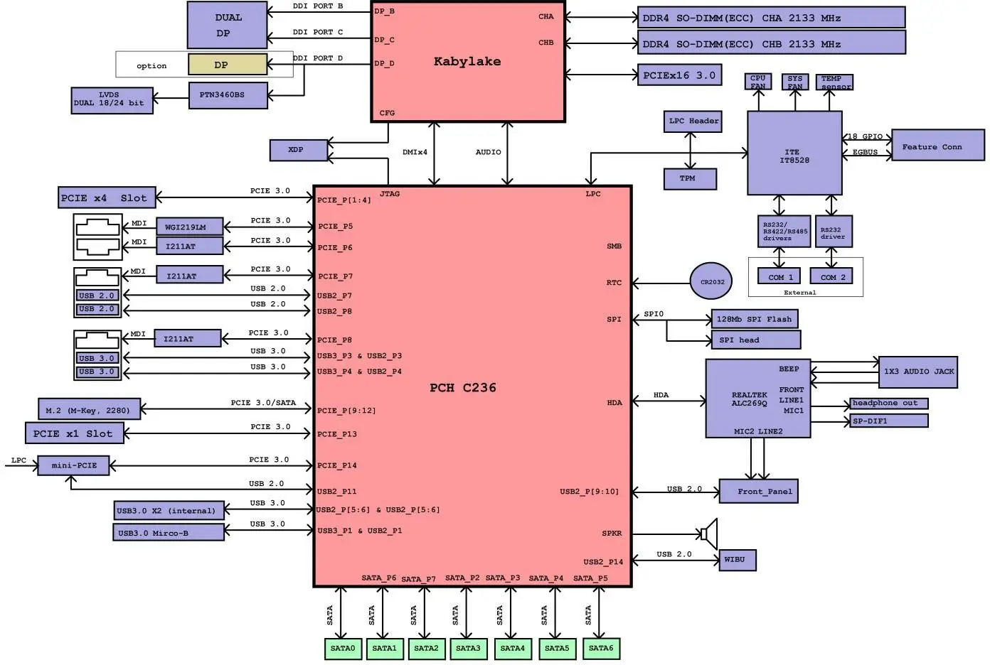
Block Diagram
Figure 1: Block Diagram of FlexATX-KBL
Component Main Data
The table below summarizes the features of the FlexATX-KBL-S embedded motherboard.
Table 1: Component Main Data
| Motherboard FlexATX-KBL-S | |
| Form factor | FlexATX with 229 mm x 191 mm (9 inch x 7.5 inch) |
| Processor | Onboard CPU variants Intel® Kabylake-S Processor line with FCLGA1151 Socket (37.5 mm x 37.53 mm), range from 65 to 80 W TDP, Kabylake processors Core™ i7-7700, Core™ i5-7500, Core™ i3-7101E, Xeon® Processor E3- 1275 v6 |
| Platform Controller Hub (PCH) | Intel®KBL Intel C236 PCH |
| Memory | 2x Dual-Channel DDR4SO-DIMM, support DDR4 (1.2 V) with 2133 MT/s (PC4-2133), Kabylake version supports up to 2400 MT/s, max. up to 32 GB memory using 2×16 GB modules |
| Storage | 4x SATA 3.0 with 6 Gb/s, 2x SATA optional, one M.2 card slot optional |
| Watchdog Timer | Implemented in embedded controller (IT8528E) |
| H/W Status Monitor | Monitoring system temperature |
| Trusted Platform Module (TPM) | Infineon SLB9665TT 2.0 and WIBU Safenet TPM |
| Power management | ACPI 4.0a C0, C1, C1E, C3, C6, C7, C8, C9, C10 states |
| Battery | CR2032, 220mAh See Safety Instructions below this table. |
| Expansion | One PCIe x16 slot (PCIe Gen3), can operate at 2.5 GT/s, 5 GT/s, or 8 GT/s, 1x PCIe x4, 1x PCIe x1 |
| Operating System Support | Windows 10 |
| External I/O | |
| LAN , USB | 4x Gbit-Ethernet RJ-45 LAN Port (with two LED indicators), dual USB3.0 and dual USB2.0 |
| Audio | 3x Audio Jacks for MIC-input, Line-out and Line-input |
| Display Port | 2x Display Port dual stack, one additional Display Port upright type |
| COM | 2 x COM Ports |
| Internal I/O | |
| SATA | 6 x SATA 3.0 (6 Gb/s) |
| PC Buzzer | Standard PC buzzer on board |
| LVDS (40-pin) | 1 x ( 2 x 20 ) 1.25 mm pin-header for 24-bit dual channel with brightness control |
| PCI | 1×16 PEG Gen3, 1x PCI x4, 1x PCI x1 |
| M.2 (M-Key, 2280) | 2x (SATA-PCIe x4/Optane Memory) |
| Mini PCIe | 1 x full size with USB 2.0 |
| Audio | 1x (1×3) S/PDIF, 1x (1×3) H/P, 1 x ( 1 x 4 ) 2.0 mm pin-header for Speaker with 2 W + 2 W amplifier |
| Internal Header | |
| Fan | 2 x (1 x 4 ) 2.54 mm pin-header for CPU & System fan with Pulse Width Modulation (PWM) function |
| CMOS Clear | 1 x (1 x 3 ) 2 mm pin-header |
| Front Panel | 1 x 2.54 mm 24 pin-header |
| Display | |
| Graphics Controller | Intel®Gen 9 LP (generation 9 Low Power) graphics core:
|
| DP to LVDS Controller | PTN3460BS |
| Display Interface | Display Port 1.2 and LVDS Note: Three (3) Independent Displays Max. |
| Resolution | DP/LVDS 4096×2304 @ 60 Hz, 24 bpp (One panel display) |
| Ethernet | |
| Controller | LAN1: Intel® I219LM 10/100/1000 Gigabit Ethernet PHY with AMT11.0 LAN2: Intel® I211AT10/100/1000 Gigabit Ethernet Controller LAN3 and LAN4 I211 LAN |
| Interface | IEEE 802.3 10BASE-T / 100BASE-TX / 1000BASE-T compliant |
| Audio | |
| HDAC | Realtek®ALC269Q High Definition Audio Codec |
| Power Supply | |
| Power Type | 4-pin ATX 12V power connector and : 20-pin or 24-pin ATX Power connector. |
![]() Danger of explosion if the lithium battery is incorrectly replaced.
Danger of explosion if the lithium battery is incorrectly replaced.
- Replace only with the same or equivalent type recommended by the manufacturer
- Dispose of used batteries according to the manufacturer’s instructions
Table 2: Environmental Conditions
| Operating | 0°C to +60°C (32°F~140°F) operating temperature (forced cooling). It is the customer’s responsibility to provide sufficient airflow around each of the components to keep them within allowed temperature range. 50 % to 90 % relative humidity (non-condensing) |
| Storage | -40°C to~70°C (-40°F~176°F); lower limit of storage temperature is defined by specification restriction of on-board CR2032 battery. Intel CPUs and PCHs only support commercial temperature ranges (0° to 60°C), but the board will be tested to extended temperatures (-25° to +70°C) with standard cooler running at maximum speed to provide overall stability report at extended temperature ranges. Absolute margin test will be performed to obtain absolute limits of the board, when the board stops to operate properly. |
| Radiated Emissions (EMI) |
|
| Shock | Follows IEC 60068-2-27. Half-sine wave, acceleration 2g, pulse duration 11ms, shock count 600 (100 per face). |
| Vibration | IAW IEC 60068-2-64, Test Fh, Random Vibration. 90 min per axis, 3 axes, at 1.9 grms, with PSD 10-20 Hz 0.05 g²/Hz and 20-500 Hz -3dB/octave. |
| Restriction of Hazardous Substances (RoHS) | All boards in the FlexATX-KBL family are RoHS compliant |
Table 3: Certification and Compliance Information
| UL | E147705-A97-UL: Equipment Including Electrical Business Equipment |
| CE | EMC Directive 2014/30/EU EN55032/EN55024 |
| FCC/ISED | 47 CFR FCC Part 15 Subpart B class B ANSI C63.4:2014 |
| CE EMC | EN 55032:2012/AC:2013 CISPR 32:2012 EN 61000-3-2:2014 EN 61000-3-3:2013 EN 55024:2010 + A1:2015 |
| Safety | EN60950-1:2006+A11:2009+A1:2010+A12:2011 |
Jumpers and Connectors
Hardware Configuration Setting
This chapter gives the definitions and shows the positions of jumpers, headers and connectors. All of the configuration jumpers on the board are in the proper position. The default settings shipped from factory are marked with an asterisk (*).
In general, jumpers on the board are used to select options for certain features. Some of the jumpers are designed to be user-configurable, allowing for system enhancement. The others are for testing purpose only and should not be altered. To select any option, cover the jumper cap over (SHORT) or remove (NC) it from the jumper pins according to the following instructions. Here, NC stands for “Not Connect”.
Connectors
Table 4: Connectors
| Connectors | Function | Remark |
| CPU_FAN | CPU FAN Connector | 1 x 4 Wafer |
| SYS_FAN | SYS FAN Connector | 1 x 4 Wafer |
| FP | Front Panel Connector | 2 x 12 Header |
| LVDS | LVDS Connector | 2 x 20 Connector |
| ATX | ATX Power Connector | 2 x 12 Connector |
| PWR_CPU1 | CPU Power Connector | 2 x 2 Connector |
| MINI-PCIE | Mini PCIe Connector | |
| PCIEx16X | PCIe x16 3.0 Connector | |
| PCIEx4x | PCIe x4 Connector | |
| PCIEx1 | PCIe x1 Connector | |
| SPI_SOCKET | Bios Socket | 2 x 4 socket |
| SPI ROM | SPI connector | 12-pin header |
| SATA1 | SATA3.0 Connector | Standard |
| SATA2 | SATA3.0 Connector | Standard |
| SATA3 | SATA3.0 Connector | Standard |
| SATA4 | SATA3.0 Connector | Standard |
| SATA5 | SATA3.0 Connector | Standard |
| SATA6 | SATA3.0 Connector | Standard |
| BAT1 | Battery Socket | CR2032 compatible |
| DIMM | Memory Socket | Slot |
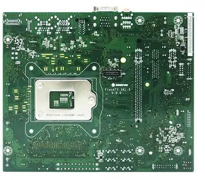
Mainboard Placement and Rear I/O locations
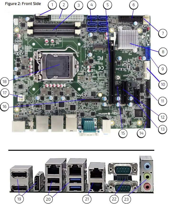
|
|
Rear Side
Pin Definitions
The following sections provide pin definitions and detailed description of all on-board connectors. The connector definitions follow the following notation:
Table 5: Connector Definitions
| Column Name | Description |
| Pin | Shows the pin-numbers in the connector. The graphical layout of the connector definition tables is made similar to the physical connectors. |
| Signal | The mnemonic name of the signal at the current pin. The notation “XX#” states that the signal “XX” is active low. |
| Type | AI: Analogue Input. AO: Analogue Output. I: Input, TTL compatible if nothing else stated. IO: Input / Output. TTL compatible if nothing else stated. IOT: Bi-directional tristate IO pin. IS: Schmitt-trigger input, TTL compatible. IOC: Input / open-collector Output, TTL compatible. IOD: Input / Output, CMOS level Schmitt-triggered. (Open drain output) NC: Pin not connected. O: Output, TTL compatible. OC: Output, open-collector or open-drain, TTL compatible. OT: Output with tri-state capability, TTL compatible. LVDS: Low Voltage Differential Signal PWR: Power supply or ground reference pins. |
| Ioh: Typical current in mA flowing out of an output pin through a grounded load, while the output voltage is > 2.4 V DC (if nothing else stated). Iol: Typical current in mA flowing into an output pin from a VCC connected load, while the output voltage is < 0.4 V DC (if nothing else stated). | |
| Pull U/D | On-board pull-up or pull-down resistors on input pins or open-collector output pins. |
| Note | Special remarks concerning the signal. |
| Designation | Type and number of item described |
| see Section | Number of section in this manual containing detailed description |
Processor Support
The FlexATX is designed to support the following processors:
- 7th generation Intel® Core i7, -i5, -i3 Quad Core processor
- Intel® Xeon processor
Kontron has defined the board versions as listed in the following table, so far all based on Embedded CPUs.
Table 6: Processor Support
| Name | Speed | Turbo | Embed. | Cache | Sspec | TDP / Tj | Part number |
| Core™ i7-7700 | 3.6 GHz | 4.2 GHz | Yes | 8 MB | SR338 | 65 W / 100ºC | 1060- 9526 |
| Core™ i5-7500 | 3.4 GHz | 3.8 GHz | Yes | 8 MB | SR335 | 65 W / 100ºC | 1060- 9525 |
| Core™ i3-7101E | 3.9 GHz | Yes | 3 MB | SR32Z | 54 W / 100ºC | 1060- 9524 | |
| Xeon™ E3-1275 V6 | 3.8 GHz | 4.2 GHz | Yes | 8 MB | SR32A | 73 W / | 1060- 9489 |
System Memory Support
The memory system has two DDR4 sockets. The sockets support the following memory features:
- 2x DDR4 SO-DIMM, 1.2 V
- Max up to 32 GB (2×16 GB).
- Dual channel, 260 pins, 1866/2133 MT/s (PC4-1866/PC4-2133)
- ECC is supported
Kontron offers the following memory modules:
Table 7: Memory Support
| Memory Module Description | Part number |
| DDR4-2133 non-ECC SODIMM 4GB | 1060-2753 |
| DDR4-2133 non-ECC SODIMM 8GB | 1060-2760 |
| DDR4-2133 non-ECC SODIMM 16GB | 1060-2761 |
| DDR4-2133 ECC SODIMM 4GB | 1060-2762 |
| DDR4-2133 ECC SODIMM 8GB | 1060-2763 |
| DDR4-2133 ECC SODIMM 16GB | 1060-2764 |
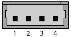
Ethernet Connectors (I/O area)
The FlexATX-KBL-S supports four channels of 10/100/1000 Mbit Ethernet.
In order to achieve the specified performance of the Ethernet port, Category 5 twisted pair cables must be used with 10/100 MByte/s and Category 5E, 6 or 6E with 1 Gbit/s LAN networks.
Figure 4: Ethernet Connector
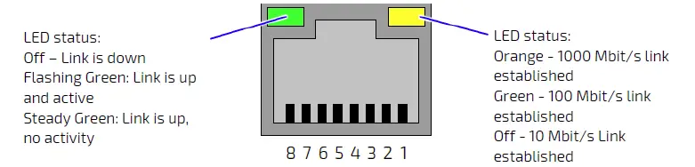
| Pin | Signal | Ethernet 10 BaseT/100BaseT | Gigabit-Ethernet |
| 1 | MDI0+ | TX+ | D1+ |
| 2 | MDI0- | TX- | D1- |
| 3 | MDI1+ | RX+ | D2+ |
| 4 | MDI1- | D3+ | |
| 5 | MDI2+ | D3- | |
| 6 | MDI2- | RX- | D2- |
| 7 | MDI3+ | D4+ | |
| 8 | MDI3- | D4- |
| Signal | Description |
| MDI[0]+ / MDI[0]- | In MDI mode, this is the first pair in 1000Base-T, i.e. the BI_DA+/- pair, and is the transmit pair in 10Base-T and 100Base-TX. In MDI crossover mode, this pair acts as the BI_DB+/- pair, and is the receive pair in 10Base-T and 100Base-TX. |
| MDI[1]+ / MDI[1]- | In MDI mode, this is the second pair in 1000Base-T, i.e. the BI_DB+/- pair, and is the receive pair in 10Base-T and 100Base-TX. In MDI crossover mode, this pair acts as the BI_DA+/- pair, and is the transmit pair in 10Base-T and 100Base-TX. |
| MDI[2]+ / MDI[2]- | In MDI mode, this is the third pair in 1000Base-T, i.e. the BI_DC+/- pair. In MDI crossover mode, this pair acts as the BI_DD+/- pair. |
| MDI[3]+ / MDI[3]- | In MDI mode, this is the fourth pair in 1000Base-T, i.e. the BI_DD+/- pair. In MDI crossover mode, this pair acts as the BI_DC+/- pair. |
USB Connectors (I/O area)
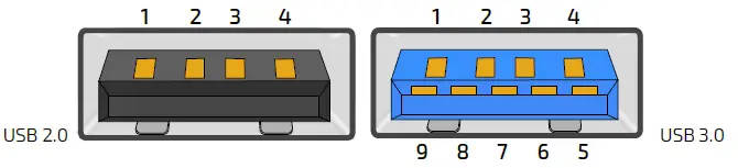
| Pin | Type | Signal | Note |
| 1 | PWR | 5 V / SB 5 V | USB2.0 / 3.0 |
| 2 | IO | USB 3- | USB2.0 / 3.0 |
| 3 | IO | USB 3+ | USB2.0 / 3.0 |
| 4 | PWR | GND | USB2.0 / 3.0 |
| 5 | IO | RX 2- | USB3.0 |
| 6 | IO | RX 2+ | USB3.0 |
| 7 | PWR | GND | USB3.0 |
| 8 | IO | TX 2- | USB3.0 |
| 9 | IO | TX 2+ | USB3.0 |
| Signal | Description |
| USBn+ USBn- RXn+ RXn- TXn+ TXn- | Differential pair works as serial differential receive/transmit data lines. (n= 0,1,2,3) |
| 5 V / SB5 V | 5 V supply for external devices. SB5 V is supplied during power-down to allow wakeup on USB device activity. Protected by resettable 2.6 A of USB3.0 and 1.5 A of USB2.0. |
For HiSpeed rates it is required to use a USB cable, which is specified in USB2.0 standard:
Figure 6: USB 2.0 High Speed Cable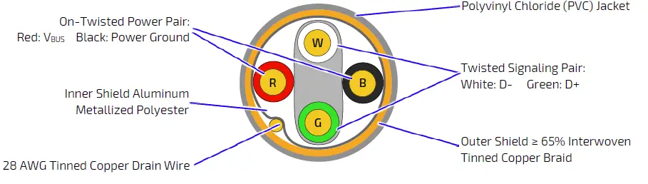
Outer Shield ≥ 65% Interwoven Tinned Copper Braid
For SuperSpeed rates it is required to use a USB cable, which is specified in USB3.0 standard:
Figure 7: USB 3.0 High Speed Cable
Fan Connector (internal, J34, J35)
The FANSYS (SYS_FAN) can be used to power, control and monitor a fan for chassis ventilation etc.
The 4-pin header is recommended to be used for driving 4-wire type fan in order to implement FAN speed control.
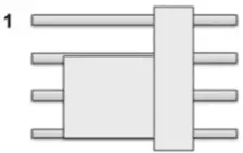
Figure 8: 4-pin Fan Connector
| Pin | Signal | Description | Type |
| 1 | PWM | FAN speed sense | O |
| 2 | TACHO | FAN speed control | I |
| 3 | 12 V | Power +12 V | PWR |
| 4 | GND | Ground | PWR |
| Signal | Description | Type |
| GND | Power Supply GND signal | PWR |
| 12 V | +12 V supply for fan. A maximum of 2000 mA can be supplied from this pin. | PWR |
| TACHO | Tacho input signal from the fan, for rotation speed supervision RPM (Rotations Per Minute). | I |
| PWM | PWM output signal for FAN speed control. | O |
Front Panel (internal)
Figure 9: FP1 Connector
| Pin | Description | Pin | Description |
| 1 | USB Port 1 VBUS | 2 | USB Port 2 VBUS |
| 3 | USB Port 1 Data- | 4 | USB Port 2 Data- |
| 5 | USB Port 1 Data+ | 6 | USB Port 2 Data+ |
| 7 | Ground | 8 | Ground |
| 9 | Not present (Key) | 10 | Headphone out left |
| 11 | Power 5.0V S0 | 12 | Power 5.0V S0 |
| 13 | SATA LED output (Active low) | 14 | Suspend LED output |
| 15 | Ground | 16 | Power button input (Active low) |
| 17 | Reset button input (Active low) | 18 | Ground |
| 19 | Power 3.3V S5 | 20 | Headphone out right |
| 21 | Analog Ground | 22 | Analog Ground |
| 23 | Microphone in left | 24 | Microphone in right |
USB3.0 Internal Header
Figure 10: USB Internal Connector

| Pin | Description | Pin | Description |
| 1 | Power | 2 | SSRX0- |
| 3 | SSRX0+ | 4 | GND |
| 5 | SSTX0- | 6 | SSTX0+ |
| 7 | GND | 8 | USB0- |
| 9 | USB0+ | 10 | NC |
| 11 | USB1+ | 12 | USB1- |
| 13 | GND | 14 | SSRT1+ |
| 15 | SSTX1- | 16 | GND |
| 17 | SSRX1+ | 18 | SSRX1- |
| Pin | Description | Pin | Description |
| 19 | Power |
Internal Feature Connector
Figure 11: GPIO Internal Connector
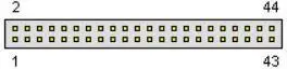
| Pin | Description | Pin | Description |
| 1 | INTRUDER# | 2 | SMBus Clock |
| 3 | SLP_S4# | 4 | SMBus Data |
| 5 | SYS_PWROK | 6 | External Battery |
| 7 | N/C | 8 | N/C |
| 9 | Power 3.3V S5 | 10 | Power 5.0V S5 |
| 11 | GPIO0 | 12 | GPIO1 |
| 13 | GPIO2 | 14 | GPIO3 |
| 15 | GPIO4 | 16 | GPIO5 |
| 17 | GPIO6 | 18 | GPIO7 |
| 19 | Ground | 20 | Ground |
| 21 | GPIO8 | 22 | GPIO9 |
| 23 | GPIO10 | 24 | GPIO11 |
| 25 | GPIO12 | 26 | GPIO13 |
| 27 | GPIO14 | 28 | GPIO15 |
| 29 | GPIO16 | 30 | GPIO17 |
| 31 | Ground | 32 | Ground |
| 33 | External GPIO Bus Clock | 34 | External GPIO Bus Chip Select (Active low) |
| 35 | External GPIO Bus Address/Data | 36 | Timer 0 |
| 37 | Power 12.0V S0 | 38 | Ground |
| 39 | N/C | 40 | N/C |
| 41 | Ground | 42 | Ground |
| 43 | Ground | 44 | SLP_S3# |
Audio Jack Connectors (I/O area)
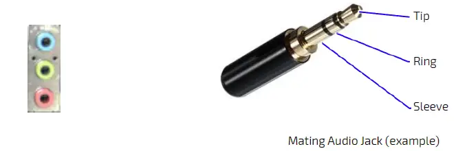
| Pin Designation | Signal | Type | Note |
| Tip | Front_L | OA | For headphone, max 1.6 VRMS |
| Ring | Front R | OA | For headphone, max 1.6 VRMS |
| Sleeve | GND | PWR |
| Pin Designation | Signal | Type | Note |
| Tip | LINE1_L | IA | 1.0 VRMS, 30 kΩ |
| Ring | LINE1_R | IA | 1.0 VRMS, 30 kΩ |
| Sleeve | GND | PWR |
| Pin Designation | Signal | Type | Note |
| Tip | |||
| Ring | |||
| Sleeve | GND | PWR |
| Signal | Description | Note |
| LINE1_L | Line In signal Left | |
| LINE1_R | Line In signal Right | |
| Front_L | Line Out Left | |
| Front_R | Line Out Right |
S/PDIF and Lineout header (internal, J31)
Figure 13: S/PDIF and Lineout Header
1 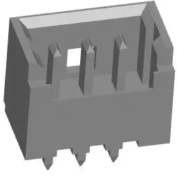
Table 8: S/PDIF
| Pin | Description |
| 1 | SPDIF_Out |
| 2 | GND |
| 3 | SPDIF_In |
LVDS (internal)
Figure 14: LVDS Connector
| Pin | Description | Pin | Description |
| 1 | Power 12.0V S0 | 2 | Power 12.0V S0 |
| 3 | Power 12.0V S0 | 4 | Power 12.0V S0 |
| 5 | Power 12.0V S0 | 6 | Ground |
| 7 | Power 5.0V S0 | 8 | Ground |
| 9 | Power LVDS Logic | 10 | Power LVDS Logic |
| 11 | DDC Clock | 12 | DDC Data |
| 13 | Backlight Control / PWM | 14 | VDD Enable |
| 15 | Backlight Enable | 16 | Ground |
| 17 | LVDS Channel A Data0- | 18 | LVDS Channel A Data0+ |
| 19 | LVDS Channel A Data1- | 20 | LVDS Channel A Data1+ |
| 21 | LVDS Channel A Data2- | 22 | LVDS Channel A Data2+ |
| 23 | LVDS Channel A Clock- | 24 | LVDS Channel A Clock+ |
| 25 | LVDS Channel A Data3- | 26 | LVDS Channel A Data3+ |
| Pin | Description | Pin | Description |
| 27 | Ground | 28 | Ground |
| 29 | LVDS Channel B Data0- | 30 | LVDS Channel B Data0+ |
| 31 | LVDS Channel B Data1- | 32 | LVDS Channel B Data1+ |
| 33 | LVDS Channel B Data2- | 34 | LVDS Channel B Data2+ |
| 35 | LVDS Channel B Clock- | 36 | LVDS Channel B Clock+ |
| 37 | LVDS Channel B Data3- | 38 | LVDS Channel B Data3+ |
| 39 | Ground | 40 | Ground |
SATA (Serial ATA) Disk Interfaces (internal)
Figure 15: SATA Connector
| Pin | Signal | Type |
| 1 | GND | PWR |
| 2 | SATA* TX+ | |
| 3 | SATA* TX- |
| 4 | GND | PWR |
| 5 | SATA* RX- | |
| 6 | SATA* RX+ | |
| 7 | GND | PWR |
| Signal | Description |
| SATA* TX+ / TX- | Host transmitter differential signal pair |
| SATA* RX+ / RX- | Host receiver differential signal pair |
specifies 0 or 1 depending on SATA port.
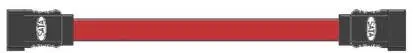
Figure 16: Available Cable Kit
SATA Internal Power(SATA_PWR1)
The SATA power connector (SATA_PWR1) supplies the SATA hard disk with either 12 V or 5 V.
Figure 17: SATA Power Internal Connector
Pin Assignment SATA Power (SATA_PWR)
| Pin | Signal |
| 1 | +12V |
| 2 | GND |
| 3 | GND |
| 4 | VCC5 |
PCIe x1 connector 1 (J2)
Figure 18: 52-pin PCIe x1 connector

| Pin | Signal | Pin | Signal |
| A1 | PRSNT1# | B1 | V_12V0_S0 |
| A2 | V_12V0_S0 | B2 | V_12V0_S0 |
| A3 | V_12V0_S0 | B3 | V_12V0_S0 |
| A4 | GND | B4 | GND |
| A5 | JTAG2_TCK | B5 | SMCLK |
| A6 | JTAG3_TDI | B6 | SMDAT |
| A7 | JTAG4_TDO | B7 | GND |
| A8 | JTAG5_TMS | B8 | V_3V3_S0 |
| A9 | V_3V3_S0 | B9 | JTAG1_TRST# |
| A10 | V_3V3_S0 | B10 | V_3V3_AUX |
| A11 | PERST# | B11 | WAKE# |
| A12 | GND | B12 | RSVD – N.C. |
| A13 | REFCLK+ | B13 | GND |
| Pin | Signal | Pin | Signal |
| A14 | REFCLK- | B14 | PET0+ |
| A15 | GND | B15 | PET0- |
| A16 | PER0+ | B16 | GND |
| A17 | PER0- | B17 | PRSNT2# |
| A18 | GND | B18 | GND |
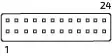
Mini PCIe Card socket
Figure 19: 52-pin Mini PCIe Card
| Pin | Signal | Pin | Signal |
| 1 | WAKE# | 2 | +3.3V_S5 |
| 3 | N.C. | 4 | GND |
| 5 | N.C. | 6 | +1.5V_S0 |
| 7 | CLKREQ# | 8 | UIM-PWR |
| 9 | GND | 10 | UIM-DATA |
| 11 | PCIe_REFCLK- | 12 | UIM-CLK |
| 13 | PCIe_REFCLK+ | 14 | UIM-RST |
| 15 | GND | 16 | UIM-VPP |
| 17 | UIM-C8 | 18 | GND |
| 19 | UIM-C4 | 20 | W_DISABLE# |
| 21 | GND | 22 | PLTRST# |
| 23 | PCIe_RX- | 24 | +3.3V_S5 |
| 25 | PCIe_RX+ | 26 | GND |
| 27 | GND | 28 | +1.5V_S0 |
| 29 | GND | 30 | PU 3.3V(S5) (Optional: SMB_CLK) |
| 31 | PCIe_TX- | 32 | PU 3.3V(S5) (Optional: SMB_DAT) |
| 33 | PCIe_TX+ | 34 | GND |
| 35 | GND | 36 | USB_D- |
| 37 | GND | 38 | USB_D+ |
| 39 | +3.3V_S5 | 40 | GND |
| Pin | Signal | Pin | Signal |
| 41 | +3.3V_S5 | 42 | PU 3.3V(S0) |
| 43 | GND | 44 | PU 3.3V(S0) |
| 45 | N.C. | 46 | PU 3.3V(S0) |
| 47 | N.C. | 48 | +1.5V_S0 |
| 49 | N.C. | 50 | GND |
| 51 | N.C. | 52 | +3.3V_S5 |
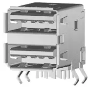
Double USB 3.0 Connector (J21)
This connector provides two USB 3.0 connections (downstream). The 5 V output is electronically fused to 900 mA each port.
Figure 20: Double USB 3.0 Connector
| Pin | Signal | Remark |
| 1 | VBUS +5V (900mA max.) | Low, Full & High Speed (USB 2.0) contact pins Bottom con. |
| 2 | USB Data – | |
| 3 | USB Data + | |
| 4 | GND | |
| 5 | USB SSRX- | Super Speed (USB3.0) contact pins Bottom con. |
| 6 | USB SSRX+ | |
| 7 | GND | |
| 8 | USB SSTX- | |
| 9 | USB SSTX+ | |
| 10 | VBUS +5V (900mA max.) | Low, Full & High Speed (USB 2.0) contact pins Top con. |
| 11 | USB Data – | |
| 12 | USB Data + | |
| 13 | GND | |
| 14 | USB SSRX- | Super Speed (USB3.0) contact pins Top con. |
| 15 | USB SSRX+ | |
| 16 | GND | |
| 17 | USB SSTX- |
| Pin | Signal | Remark |
| 18 | USB SSTX+ | |
| Shield | Shield |
DP connector (J12)
Figure 21: 20-pin DP connector
| Pin | Signal | Pin | Signal |
| 1 | ML LANE 0+ | 2 | GND (ML LANE 0) |
| 3 | ML LANE 0- | 4 | ML LANE 1+ |
| 5 | GND (ML LANE 1) | 6 | ML LANE 1- |
| 7 | ML LANE 2+ | 8 | GND (ML LANE 2) |
| 9 | ML LANE 2- | 10 | ML LANE 3+ |
| 11 | GND (ML LANE 3) | 12 | ML LANE 3- |
| 13 | AUX_SEL# | 14 | Pull-down to GND |
| 15 | AUX CH+ | 16 | GND (AUX CH) |
| 17 | AUX CH- | 18 | Hot plug |
| 19 | GND (GND_DDC) | 20 | +3.3V (DDC EEPROM power) Max 500mA |
RTC battery holder
Figure 22: RTC battery holder
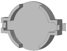
| Pin | Signal |
| Positive (+) | V_BAT_INT |
| Negative (-) | GND |
Module Power-In Connector
Figure 23: Module Power-In Connector

| Pin | Signal | Description |
| 1 | V_MODULE | Module Power 3.0 V to 5.25 V may be independent of Carrier power. |
| 2 | GND | |
| 3 | N.C. | Not connected |
| 4 | GND |
Internal Power Connector
Figure 24: Internal Power Connector

| Pin | Signal | Pin | Signal |
| 1 | Power Input 3.3V S0 | 13 | Power Input 3.3V S0 |
| 2 | Power Input 3.3V S0 | 14 | Power Input -12.0V S0 |
| 3 | Ground | 15 | Ground |
| 4 | Power Input 5.0V S0 | 16 | ATX PS_ON# Signal |
| 5 | Ground | 17 | Ground |
| 6 | Power Input 5.0V S0 | 18 | Ground |
| 7 | Ground | 19 | Ground |
| 8 | ATX Power Good signal | 20 | Power Input -5.0V S0 |
| 9 | Power Input 5.0V S5 | 21 | Power Input 5.0V S0 |
| Pin | Signal | Pin | Signal |
| 10 | Power Input 12.0V S0 | 22 | Power Input 5.0V S0 |
| 11 | Power Input 12.0V S0 | 23 | Power Input 5.0V S0 |
| 12 | Power Input 3.3V S0 | 24 | Ground |
Recommended Power Supply for KabyLake motherboard should be above or equal to 473 W.
 PS/2 Header (J30)
Figure 25: PS/2 Header
1 
| Pin | Signal |
| 1 | Keyboard Clock |
| 2 | Keyboard Data |
| 3 | Mouse Clock |
| 4 | Mouse Data |
| 5 | Power 5.0V S5 |
| 6 | Ground |
LPC Header (J33)
Figure 26: 20-pin LPC Header

| Pin | Signal | Pin | Signal |
| 1 | LPC Clock (33MHz) | 2 | Ground |
| 3 | LPC Frame# | 4 | Not present (Key) |
| 5 | Platform Reset (PLTRST#) | 6 | Power 5.0V S0 |
| 7 | LPC LAD3 | 8 | LPC LAD2 |
| Pin | Signal | Pin | Signal |
| 9 | Power 3.3V S0 | 10 | LPC LAD1 |
| 11 | LPC LAD0 | 12 | Ground |
| 13 | SMBus Clock | 14 | SMBus Data |
| 15 | Power 3.3V S0 | 16 | SERIRQ |
| 17 | Ground | 18 | N/C |
| 19 | N/C | 20 | N/C |
SPI External Flash header (J36)
Figure 27: 12-pin SPI Header

| Pin | Signal | Pin | Signal |
| 1 | SPI Clock | 2 | Power 3.3V S5 |
| 3 | SPI CS# | 4 | SPI ADDIN |
| 5 | Power 3.3V S5 | 6 | N/C |
| 7 | SPI MOSI | 8 | SPI ISOLATE |
| 9 | SPI MISO | 10 | Ground |
| 11 | SPI IO2 | 12 | SPI IO3 |
SPI External GPIO header (J37)
Figure 28: 12-pin GPIO Header
| Pin | Signal | Pin | Signal |
| 1 | SPI Clock | 2 | Power 3.3V S5 |
| 3 | SPI CS# | 4 | SPI ADDIN |
| 5 | Power 3.3V S5 | 6 | N/C |
| Pin | Signal | Pin | Signal |
| 7 | SPI MOSI | 8 | SPI ISOLATE |
| 9 | SPI MISO | 10 | Ground |
| 11 | SPI IO2 | 12 | SPI IO3 |
RS-232/RS-485, RS-422 Header
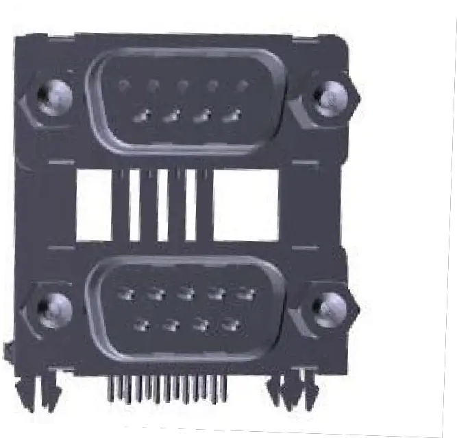
| Pin | RS232 | RS422/RS485 Full Duplex | RS 485 Half duplex |
| 1 | DCD | Tx- | Data- |
| 2 | RxD | Tx+ | Data+ |
| 3 | TxD | Rx+ | |
| 4 | DTR | Rx- | |
| 5 | GND | GND | GND |
| 6 | DSR | ||
| 7 | RTS | ||
| 8 | DCTS | ||
| 9 | RI |
Figure 29: 9-pin RS-232 Header (upper connector), 9-pin RS-232/RS-485/RS-422 Header (lower connector) Table 9: RS232, RS485/RS422 Connector
| Signal | Description |
| TxD | Transmitted Data, sends data to the communications link. The signal is set to the marking state (-12 V) on hardware reset when the transmitter is empty or when loop mode operation is initiated. |
| RxD | Received Data, receives data from the communications link. |
| DTR | Data Terminal Ready, indicates to the modem etc. that the on-board UART is ready to establish communication link. |
| DSR | Data Set Ready, indicates that the modem etc. is ready to establish a communications link. |
| RTS | Request To Send, indicates to the modem etc. that the on-board UART is ready to exchange data. |
| CTS | Clear To Send, indicates that the modem or data set is ready to exchange data. |
| DCD | Data Carrier Detect, indicates that the modem or data set has detected the data carrier. |
| Signal | Description |
| RI | Ring Indicator, indicates that the modem has received a ringing signal from the telephone line. |
RS-485/422: Receiver Termination enabled
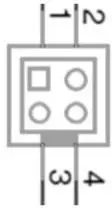
RTC/SRTC Reset Jumper (J45, J46)
Figure 30: 2-pin RTC Reset Jumper

RTC Reset Jumper (J45)
| Pin | Signal |
| 1 | RTCRST# |
| 2 | Ground |
SRTC Reset Jumper (J46)
| Pin | Signal |
| 1 | SRTCRST# |
| 2 | Ground |
Indicators
Attached Indicators List
Table 10: LEDs internal
| Part | Indicator | Function |
| J2 | Upper Port Left LED | GbE Link / Activity |
| Upper Port Right LED | GbE Speed 100/1000 | |
| Lower Port Left LED | GbE Link / Activity | |
| Lower Port Right LED | GbE Speed 100/1000 | |
| J3 | Left LED | GbE Link / Activity |
| Right LED | GbE Speed 100/1000 | |
| J4 | Left LED | GbE Link / Activity |
| Right LED | GbE Speed 100/1000 |
External indicators list
Table 11: External Indicators
| Location | Indicator | Function |
| J25 | SATA LED# | SATA Activity LED |
| SUS LED | Suspend state LED |
System Status LED
Table 12: System Status LEDs
| System state | Red LED Status | Green LED Status | Color |
| S0 | Off | On | Green |
| S3 | Blink @1Hz | Blink @1Hz | Yellow |
| S5 | On | On | Yellow |
| Overheat below limit | Blink @1Hz | Off | Red |
| Overheat above limit | On | Off | Red |
| G3 / Error state | Off | Off |
BIOS Setup structure
The Setup utility features for menus listed in the selection bar at the top of the screen:
- Main
- Advanced
- Chipset
- Security
- Boot
- Save & Exit
The Setup menus are selected via the left and right arrow keys. The currently active menu and the currently active uEFI BIOS Setup item are highlighted in white. Each Setup menu provides two main frames. The left frame displays all available functions. Functions that can be configured are displayed in blue. Functions displayed in gray provide information about the status or the operational configuration. The right frame displays an Item Specific Help window providing an explanation of the respective function.
Main Setup Menu
Upon entering the uEFI BIOS Setup program, the Main Setup menu is displayed. This screen lists the Main Setup menu sub-screens and provides basic system information as well as functions for setting the system time and date.
Table 13: Main Setup Menu Sub-Screens Functions
| Sub-Screen/Function | Description |
| BIOS Information | Display BIOS Vendor, Core Version, and etc. |
| Board Information | Display Product Name, PCB ID, and etc. |
| Processor Information | Display Name, Type, Speed, and etc. |
| PCH Information | Display Name, PCH SKU, and etc. |
| System Language | Set System Language |
| System Date | Set System Date |
| System Time | Set System Time |
Advanced Setup Menu
The Advanced Setup menu provides sub-screens and functions for advanced configuration.
Table 14: Advanced Setup Menu Sub-Screens and Functions
| Sub-Screen | Function | Description |
| Intel RC ACPI Settings | PTID Support | Enable/Disable PTID Support |
| PECI Access Method | Direct I/O or ACPI PECI Access Method | |
| Native PCIE Enable | Enable/Disable Native PCIE Enable | |
| Native ASPM | Auto/Enable/Disable Controlled ASPM | |
| BDAT ACPI Table Support | Enable/Disable BDAT ACPI Table Support | |
| Wake system from S5 | Enable/Disable system wake on alarm event |
| Sub-Screen | Function | Description |
| ACPI Debug | Enable/Disable ACPI Debug | |
| Low Power SO Idle | Enable/Disable Low Power SO Idle | |
| Lpit Recidency Counter | Select Recidency Counter | |
| PCI Delay Optimization | Enable/Disable PCI Delay Optimization | |
| ZpODD | Enable/Disable ZpODD | |
| CPU Configuration | C6DRAM | Enable/Disable C6DRAM |
| SW Guard Extensions (SGX) | Enable/Disable Software Guard Extensions (SGX) | |
| Select Owner EPOCH input type | There are three owner EPOCH modes (No Change in Owner EPOCHs; Change to New Random Owner EPOCHs; Manual User Defined Owner EPOCHs) | |
| PRMRR Size | Display the PRMRR | |
| CPU Flex Ratio Override | Enable/Disable CPU Flex Ratio Override | |
| CPU Flex Ratio Settings | Display the CPU Flex Ratio Settings | |
| Hardware Prefetcher | Enable/Disable Hardware Prefetcher | |
| Adjacent Cache Line Prefetch | To turn on/off prefetching of adjacent cache lines | |
| Intel (VMX) Virtualization Technology | Enable/Disable Intel (VMX) Virtualization Technology | |
| PECI | Enable/Disable PECI | |
| Active Processor Core | Number of cores to enable in each processor package | |
| BIST | Enable/Disable BIST (Built-In Self Test) on reset | |
| JTAG C10 Power | Enable/Disable Power JTAG in C10 and deeper power states | |
| AP threads Idle Manner | Ap thread Idle Manner for waiting signal to run | |
| AP threads Handoff Manner | AP threads Handoff to OS Manner from end of POST | |
| AES | Enable/Disable AES (Advance Encryption Standard) | |
| MachineCheck | Enable/Disable Machine Check | |
| MonitorMWait | Enable/Disable MonitorMWait | |
| Intel Trusted Execution Technology | Enable utilization of additional hardware capabilities provided by Intel (R) Trusted Execution Technology | |
| Alias Check Request DPR Memory Size (MB) | Display Alias Check Request DPR Memory Size (MB) | |
| Reset AUX Content | Reset TPM Aux content. Txt may not |
| Sub-Screen | Function | Description | |||
| functional after AUX content gets reset | |||||
| Flash Wear Out Protection | Enable/Disable Flash Wear Out Protection | ||||
| Current Debug Interface Status | Display Current Debug Interface Status | ||||
| Debug Interface | Enable/Disable Debug Interface Support | ||||
| Debug Interface Lock | Enable/Disable Debug Interface Lock | ||||
| Processor trace memory allocation | Disable or select processor trace memory region size: from 4KB ~ 128MB | ||||
| CPU SMM Enhancement | SMM Code Access Check | Enable/Disable support for SMM Code Access feature | |||
| SMM Use Delay Indication | Enable/Disable usage of SMM_DELAYED MSR for MP sync in SMI | ||||
| SMM Use Block Indication | Enable/Disable usage of SMM_BLOCKED MSR for MP sync in SMI | ||||
| FCLK Frequency for Early Power On | FCLK can take values of 400MHz, 800MHz and 1GHZ | ||||
| Voltage Optimization | Enable/Disable/Auto Voltage Optimization | ||||
| Power & Performance | CPU – Power Managemen t Control | Boot Performance mode | Select the performance state that the BIOS will set starting from reset vector | ||
| Intel (R) SpeedStep(tm) | Allows more than two frequency to be supported | ||||
| Race To Halt (RTH) | Enable/Disable Race To Halt | ||||
| Intel (R) Speed Shift Technology | Enable/Disable Intel (R) Speed Shift Technology support | ||||
| HDC Control | This option allows HDC configuration | ||||
| Turbo Mode | Enable/Disable processor Turbo Mode | ||||
| View/Configure Turbo Options | Energy Efficient P- State | Enable/Disable Energy Efficient P-State feature | |||
| Package Power Limit MSR Lock | Enable/Disable locking of Package Power Limit | ||||
| 1-Core Ratio Limit Override | Display 1-Core Ratio Limit Override | ||||
| 2-Core Ratio Limit Override | Display 2-Core Ratio Limit Override | ||||
| 3-Core Ratio Limit Override | Display 3-Core Ratio Limit Override | ||||
| 4-Core Ratio Limit Override | Display 4-Core Ratio Limit Override | ||||
| Energy Efficient Turbo | Enable/Disable Energy Efficient Turbo Feature | ||||
| Config TDP | Configurable TDP | Configurable TDP Mode as | |||
| Sub-Screen | Function | Description | |||
| Configurations | Boot Mode | Nominal/Up/Down/Deactivate TDP selection | |||
| Configurable TDP Lock | Enable/Disable Configurable TDP Lock | ||||
| CTDP BIOS Control | Enable/Disable CTDP Control via | ||||
| runtime ACPI BIOS methods | |||||
| ConfigTDP Levels | ConfigTDP Turbo Activation Ratio, Power Limit 1, Power Limit 2 | ||||
| Custom Settings | Setting for Power Limit 1, Power Limit 2, | ||||
| Nominal ConfigTDP Nominal | Power Limit 1 Time Window, ConfigTDP Turbo Activation Ratio | ||||
| Custom Settings | Setting for Power Limit 1, Power Limit 2, | ||||
| Down ConfigTDP Level 1 | Power Limit 1 Time Window, ConfigTDP Turbo Activation Ratio | ||||
| Custom Settings Up | Setting for Power Limit 1, Power Limit 2, | ||||
| ConfigTDP Level 2 | Power Limit 1 Time Window, ConfigTDP Turbo Activation Ratio | ||||
| CPU VR Settings | PSYS Slope | Display PSYS Slope | |||
| PSYS Offset | Display PSYS Offset | ||||
| PSYS Pmax Power | Display PSYS Pmax Power | ||||
| Acoustic | Acoustic | Enable/Disable Acoustic Noise | |||
| Noise Settings | Noise Mitigatio n | Mitigation | |||
| IA VR Domain | Display Disable Fast PKG C State Ramp for IA Domain and Slow Slew Rate for IA Domain | ||||
| GT VR | Display Disable Fast PKG C State Ramp | ||||
| Domain | for GT Domain and Slow Slew Rate for GT Domain | ||||
| SA VR Domain | Display Disable Fast PKG C State Ramp for SA Domain and Slow Slew Rate for SA Domain | ||||
| Core/IA | VR Config | Enable/Disable VR Config | |||
| VR Settings | Enable | ||||
| AC Loadline | Display AC Loadline | ||||
| DC | Display DC Loadline | ||||
| Loadline | |||||
| PS | Display PS Current Threshold1 | ||||
| Current | |||||
| Threshol d1 | |||||
| PS | Display PS Current Threshold2 | ||||
| Sub-Screen | Function | Description | |||
| Current | |||||
| Threshol d2 | |||||
| PS | Display PS Current Threshold3 | ||||
| Current | |||||
| Threshol d3 | |||||
| PS3 | Enable/Disable PS3 | ||||
| Enable | |||||
| PS4 Enable | Enable/Disable PS4 | ||||
| IMON | Display IMON Slope | ||||
| Slope | |||||
| IMON Offset | Display IMON Offset | ||||
| IMON | Set the Offset value as positive or | ||||
| Prefix | negative | ||||
| VR | Display VR Current Limit | ||||
| Current Limit | |||||
| VR | Display VR Voltage Limit | ||||
| Voltage Limit | |||||
| TDC Enable | Enable/Disable TDC | ||||
| TDC | Display TDC Current Limit | ||||
| Current Limit | |||||
| TDC Time Windows | TDC Time Window, value in milliseconds. 1ms is default. Range from | ||||
| 1ms to 10ms, except for 9ms as it has no valid encoding in the MSR definition | |||||
| TDC Lock | Enable/Disable TDC Lock | ||||
| GT- UnSliced | VR Config Enable | Enable/Disable VR Config | |||
| VR Settings | |||||
| AC Loadline | Display AC Loadline | ||||
| DC Loadline | Display DC Loadline | ||||
| PS | Display PS Current Threshold1 | ||||
| Current | |||||
| Threshol d1 | |||||
| PS | Display PS Current Threshold2 | ||||
| Current | |||||
| Threshol | |||||
| Sub-Screen | Function | Description | |||
| d2 | |||||
| PS | Display PS Current Threshold3 | ||||
| Current | |||||
| Threshol d3 | |||||
| PS3 | Enable/Disable PS3 | ||||
| Enable | |||||
| PS4 Enable | Enable/Disable PS4 | ||||
| IMON | Display IMON Slope | ||||
| Slope | |||||
| IMON Offset | Display IMON Offset | ||||
| IMON | Set the Offset value as positive or | ||||
| Prefix | negative | ||||
| VR | Display VR Current Limit | ||||
| Current Limit | |||||
| VR | Display VR Voltage Limit | ||||
| Voltage Limit | |||||
| TDC Enable | Enable/Disable TDC | ||||
| TDC | Display TDC Current Limit | ||||
| Current Limit | |||||
| TDC Time Windows | TDC Time Window, value in milliseconds. 1ms is default. Range from | ||||
| 1ms to 10ms, except for 9ms as it has no valid encoding in the MSR definition | |||||
| TDC Lock | Enable/Disable TDC Lock | ||||
| GT- Sliced | VR Config Enable | Enable/Disable VR Config | |||
| VR Settings | |||||
| AC Loadline | Display AC Loadline | ||||
| DC Loadline | Display DC Loadline | ||||
| PS | Display PS Current Threshold1 | ||||
| Current | |||||
| Threshol d1 | |||||
| PS | Display PS Current Threshold2 | ||||
| Current | |||||
| Threshol d2 | |||||
| Sub-Screen | Function | Description | |||
| PS Current Threshol d3 | Display PS Current Threshold3 | ||||
| PS3 Enable | Enable/Disable PS3 | ||||
| PS4 Enable | Enable/Disable PS4 | ||||
| IMON Slope | Display IMON Slope | ||||
| IMON Offset | Display IMON Offset | ||||
| IMON Prefix | Set the Offset value as positive or negative | ||||
| VR Current Limit | Display VR Current Limit | ||||
| VR Voltage Limit | Display VR Voltage Limit | ||||
| TDC Enable | Enable/Disable TDC | ||||
| TDC Current Limit | Display TDC Current Limit | ||||
| TDC Time Windows | TDC Time Window, value in milliseconds. 1ms is default. Range from 1ms to 10ms, except for 9ms as it has no valid encoding in the MSR definition | ||||
| TDC Lock | Enable/Disable TDC Lock | ||||
| VR Mailbox Command options | Display VR Mailbox Command options | ||||
| Platform PL1 Enable | Enable/Disable Platform Power Limit 1 Programming | ||||
| Platform PL2 Enable | Enable/Disable Platform Power Limit 2 Programming | ||||
| Power Limit 4 Override | Enable/Disable Power Limit 4 Override | ||||
| C States | Enable/Disable CPU Power Management | ||||
| Enhanced C-states | Enable/Disable C1E | ||||
| C-State Auto Demotion | Configure C-State Auto Demotion | ||||
| C-State Un-demotion | Configure C-State Un-demotion | ||||
| Package C-State Demotion | Enable/Disable Package C-State Demotion | ||||
| Sub-Screen | Function | Description | ||
| Package C-State Un-demotion | Enable/Disable Package C-State Un- demotion | |||
| Cstate Pre-Wake | Enable/Disable Cstate Pre-Wake | |||
| IO MWAIT Redirection | When set, will map IO_read instructions sent to IO registers PMG_IO_BASE_ADDRBASE+off set to MWAIT(offset) | |||
| Package C State Limit | Maximum Package C State Limit Setting | |||
| C3 Latency Control (MSR 0X60A) | Setting of Time Unit (Unit of measurement for IRTL value) and Latency | |||
| C6/7 Short Latency Control (MSR 0X60B) | Setting of Time Unit (Unit of measurement for IRTL value) and Latency | |||
| C6/7 Long Latency Control (MSR 0X60C) | Setting of Time Unit (Unit of measurement for IRTL value) and Latency | |||
| Thermal Monitor | Enable/Disable Thermal Monitor | |||
| Interrupt Redirection Mode Selection | Interrupt Redirection Mode Select for Logical Interrupts | |||
| Timed MWAIT | Enable/Disable Timed MWAIT | |||
| Custom P-state Table | Display Number of P states | |||
| Energy performance gain | Enable/Disable Energy performance gain | |||
| EPG DIMM Idd3N | Display EPG DIMM Idd3N | |||
| EPG DIMM Idd3P | Display EPG DIMM Idd3P | |||
| Power Limit 3 Settings | Enable/Disable Power Limit 3 Override | |||
| CPU Lock Configuration | CFG Lock | Configure MSR 0XE2[15], CFG Lock bit | ||
| Overclocking Lock | Enable/Disable Overclocking Lock | |||
| GT – Power Managemen t Control | RC6 (Render Standby) | Check to enable render standby support | ||
| Maximum GT frequency | Choose between 350MHz (RPN) and 1000MHz (RPO). Value beyond the range will be clipped to min/max supported by SKU | |||
| PCH-FW Configuration | ME Firmware Version | Display ME Firmware Version | ||
| ME Firmware Mode | Display ME Firmware Mode | |||
| ME Firmware SKU | Display ME Firmware SKU | |||
| ME File System Integrity Value | Display ME File System Integrity Value | |||
| ME Firmware Status 1 | Display ME Firmware Status 1 | |||
| ME Firmware Status 2 | Display ME Firmware Status 2 | |||
| NFC Support | Display NFC Support | |||
| Sub-Screen | Function | Description | ||
| ME State | Display ME State | |||
| Manageability | Display Manageability | |||
| Features State | Display Features State | |||
| AMT BIOS Features | Display AMT BIOS Features | |||
| AMT Configuration | ASF support | Enable/Disable Alert Standard Format Support | ||
| USB Provisioning of AMT | Enable/Disable of AMT USB Provisioning | |||
| CIRA Configuration | Active Remote Assistance Process | Trigger CIRA boot | ||
| CIRA Timeout | Display CIRA Timeout | |||
| ASF Configuration | PET Progress | Enable/Disable PET Events Progress to receive PET Events | ||
| Watchdog | Enable/Disable Watchdog Timer | |||
| OS Timer | Display OS Timer | |||
| BIOS Timer | Display BIOS Timer | |||
| Secure Erase Configuration | Secure Erase Mode | Change Secure Erase module behavior | ||
| Force Secure Erase | Force Secure Erase on next boot | |||
| OEM Flags Settings | MEBx hotkey Pressed | Enable/Disable MEBx hotkey Pressed | ||
| MEBx Selection Screen | Enable/Disable MEBx Selection Screen | |||
| Hide Unconfigure ME Confirmation Prompt | Enable/Disable Hide Unconfigure ME Confirmation Prompt | |||
| MEBx OEM Debug Menu Enable | Enable/Disable MEBx OEM Debug Menu | |||
| Unconfigure ME | Enable/Disable Unconfigure ME | |||
| MEBx Resolution Settings | Non-UI Mode Resolution | Resolution for non-UI text mode | ||
| UI Mode Resolution | Resolution for UI text mode | |||
| Sub-Screen | Function | Description | |||
| Graphic Mode Resolution | Resolution for graphics mode | ||||
| ME Unconfig on RTC Clear | Display ME Unconfig on RTC Clear | ||||
| Comms Hub Support | Enable/Disable support for Comms Hub | ||||
| JHI Support | Enable/Disable Intel® DAL Host Interface Service (JHI) | ||||
| Core Bios Done Message | Enable/Disable Core Bios Done message sent to ME | ||||
| Firmware Update Configuration | Enable/Disable Me FW Image Re-Flash function | ||||
| PTT Configuration | PTT Capability/State | Display PTT Capability/State | |||
| TPM Device Selection | Selects TPM device: PTT or dTPM | ||||
| PTP aware OS | Display PTP aware OS | ||||
| ME Debug Configuration | HECI Timeouts | Enable/Disable HECI Send/Receive Timeouts | |||
| Force ME DID Init Status | Force the DID Initialization Status value | ||||
| CPU Replaced Polling Disable | Setting this option disables CPU replacement polling loop | ||||
| ME DID Message | Enable/Disable ME DID Message | ||||
| HECI Retry Disable | Setting this option disables retry mechanism for all HECI APIs | ||||
| HECI Message check Disable | Setting this option disables message check for Bios Boot Path when sending | ||||
| MBP HOB Skip | Setting this option will skip MBP HOB | ||||
| HECI2 Interface Communication | Adds and Removes HECI2 Device from PCI space | ||||
| KT Device | Enable/Disable KT Device | ||||
| IDER Device | Enable/Disable IDER Device | ||||
| End Of Post Message | Enable/Disable End Of Post Message sent to ME | ||||
| DOI3 Setting for HECI Disable | Setting this option disables setting DOI3 bit for all HECI devices | ||||
| RTD3 settings | RTD3 Support | Enable/Disable Runtime D3 Support | |||
| VR Staggering delay | Delay between subsequent VR power on to avoid current spike | ||||
| VR Ramp up delay | Delay between subsequent VR ramp ups if they are all turn ON at the same time | ||||
| PCIE Slot 5 Device Power-on delay in ms | Delay between applying core power and Deasserting PERST# | ||||
| PCIE Slot 5 Device Power-off delay in ms | Delay after removing core power | ||||
| Sub-Screen | Function | Description |
| Audio Delay | Delay after applying power to HD Audio(Realtex) codec device | |
| I2C0 Controller | Delay in _PSO I2C0 Controller | |
| SensorHub | Delay after applying power to SensorHub device | |
| I2C1 Controller | Delay in _PSO I2C1 Controller | |
| TouchPad | Delay after applying power to TouchPad device | |
| TouchPanel | Delay in PR _ON after applying power to TouchPanel device | |
| P-state Capping | Set _PPC and send ACPI notification | |
| USB Port 1 | USB RTD3 support | |
| USB Port 2 | USB RTD3 support | |
| I2C0 Sensor Hub | Enable RTD3 support for I2C0 Sensor Hub | |
| ZPODD | Zero power ODD option is applicable only for WhiteTipMountain1 and AdenHills with ZPODD Feature rework | |
| WWAN | Enable/Disable RTD3 support for WWAN | |
| Sata Port 0 | Setup option to control the SATA port RTD3 functionality | |
| Sata Port 1 | Setup option to control the SATA port RTD3 functionality | |
| Sata Port 2 | Setup option to control the SATA port RTD3 functionality | |
| MiniCard SATA Port3 | Setup option to control the SATA port RTD3 functionality | |
| Sata Port 4 | Setup option to control the SATA port RTD3 functionality | |
| PCIe Remapped CR1 | Display PCIe Remapped CR1 | |
| PCIe Remapped CR2 | Display PCIe Remapped CR2 | |
| PCIe Remapped CR3 | Display PCIe Remapped CR3 | |
| RST Raid Volumes | Valid only with RST Storage Driver | |
| OverClocking Performance Menu | OverClocking Feature | Performance Menu for Processor and Memory |
| WDT Enable | Enable/Disable WatchDog Timer | |
| RSR | Enable/Disable RSR Feature | |
| Intel ICC | ICC/OC WatchDog Timer | Enable/Disable ICC/OC WatchDog Timer |
| ICC Locks after EOP | Display ICC Locks after EOP | |
| ICC Profile | Display ICC Profile |
| Sub-Screen | Function | Description | |
| ACPI Settings | Enable ACPI Auto Configuration | Enable/Disable BIOS ACPI Auto Configuration | |
| Enable Hibernation | Enable/Disable System ability to Hibernate | ||
| ACPI Sleep State | Select the highest ACPI sleep state the system will enter when the SUSPEND button is pressed | ||
| Lock Legacy Resources | Enable/Disable Lock Legacy Resources | ||
| S3 Video Repost | Enable/Disable S3 Video Repost | ||
| SMART Settings | SMART Self Test | Run SMART Self Test on all HDDs during POST | |
| IT8528 Super IO Configuration | Super IO Chip | IT8528 | |
| Serial Port 1 Configuration | Serial Port | Enable/Disable Serial Port (COM) | |
| Device Settings | Display Device Settings | ||
| Change Settings | Select an optimal settings for Super IO Device | ||
| RS485 Duplex Mode | Sets full or or half duplex mode | ||
| Termination Control | Select COM1 receiver termination | ||
| Direction Control | Select COM1 direction | ||
| Serial Port 2 Configuration | Serial Port | Enable/Disable Serial Port (COM) | |
| Device Settings | Display Device Settings | ||
| Change Settings | Select an optimal settings for Super IO Device | ||
| Serial Port Console Redirection | Console Redirection | Enable/Disable Console Redirection | |
| Console Redirection Settings | Terminal Type | Emulation: ANSI: Extended ASCII char set. VT100: ASCII char set. VT100+: Extends VT100 to support color, function keys, etc. VT-UTF8: Uses UTF8 encoding to map Unicode | |
| Bits per second | Select serial port transmission speed | ||
| Data Bits | Data Bits | ||
| Parity | A parity bit can be sent with the data bit to detect some transmission errors | ||
| Stop Bits | Stops bits indicate the end of a serial data packet | ||
| Flow Control | Flow control can prevent data loss from buffer overflow | ||
| VT-UTF8 Combo Key Support | Enable VT-UTF8 Combination Key Support for ANSI/VT100 terminals | ||
| Recorder Mode | With this mode enable only text will be sent. This is to capture terminal data | ||
| Sub-Screen | Function | Description | |
| Resolution 100×31 | Enables/Disables extended terminal resolution | ||
| Legacy OS Redirection Resolution | On Legacy OS, the number of rows and columns supported redirection | ||
| Putty KeyPad | Select function key and keypad on Putty | ||
| Redirection After BIOS POST | The settings specify if bootLoader is selected then Legacy console redirection is disable before booting to Legacy OS | ||
| COM1(Pci Bus0, Dev0, Func0) | Enable | ||
| Console Redirection | Port is disable | ||
| Legacy Console Redirection Settings | Legacy Serial Redirection Port | Select a COM port to display redirection of Legacy OS and Legacy OPROM Messages | |
| Serial Port for Out-of-Band Management/Windows Emergency Management Services (EMS) Console Redirection | Enable/Disable Console Redirection | ||
| AMI Graphic Output Protocol Policy | Intel (R) GOP Driver | Shows GOP Driver Version | |
| Output Select | Output Interface | ||
| PCI Subsystem settings | AMI PCI Driver Version | Shows AMI PCI Driver Version | |
| Above 4G Decoding | Enable/Disable Above 4G Decoding | ||
| Hot-Plug Support | Hot-Plug Support | ||
| Restore PCIE Registers | Enable/Disable Restore PCIE Registers | ||
| Don’t Reset VC-TC Mapping | Enable/Disable Don’t Reset VC-TC Mapping | ||
| Network Stack Configuration | Network Stack | Enable/Disable UEFI Network Stack | |
| CSM Configuration | CSM Support | Enable/Disable Compatibility Support Module | |
| NVMe Configuration | NVMe controller and Device information | No NVMe Device Found | |
| USB Configuration | Legacy USB Support | Enables Legacy USB support | |
| XHCI Hand-off | This is a workaround for OSes without XHCI hand-off support | ||
| USB Mass Storage Driver Support | Enable/Disable USB Mass Storage Driver Support | ||
| Port 60/64 Emulation | Enable/Disable Port 60/64 Emulation | ||
| USB transfer time-out | The time-out value for Control, Bulk, and Interrupt transfer | ||
| Device reset time-out | USB mass storage device start unit | ||
| Sub-Screen | Function | Description |
| command time-out | ||
| Device power-up delay | Maximum time for the device will take before it properly report itself to the Host Controller | |
| LVDS Configuration | LVDS Flat Panel Display Support | Enable/Disable LVDS Flat Panel Display Support |
| Panel Type | Select the type or Manufacturer’s name of the display panel | |
| Resolution | Select the screen resolution of the display panel | |
| Panel Color Depth | Select the display panel color depth | |
| Panel Voltage | Select the voltage level for powering the LVDS Display Panel | |
| Channel | Select LVDS Interface Signals mode Single-Channel or Dual-Channel (Sometimes called “Single-Pixel” or “Dual-Pixel”) | |
| Bus Swapping | Swap LVDS interface signals: Normal – use bus as indicated by pin name, Swapped – swap odd bus signals with even bus signals | |
| Clock Frequency Center Spread | Programmable center spreading of pixel clock frequency to minimize EMI | |
| Differential Output Swing Level | Programmable LVDS signal swing to pre-compensate for channel attenuation or allow for power saving | |
| Backlight | Enable/Disable Backlight | |
| Backlight Signal Inversion | Enable – Active High Disable – Active Low for display panel Backlight signal | |
| Backlight PWM Frequency | Set the PWM frequency the backlight | |
| Brightness Level | Select the Brightness Level for the backlight of the display panel | |
| Hardware Health Configuration | System Temperature | Display the System Temperature |
| System Temperature Offset | Adjust the offset value in C (Two’s Complement) | |
| CPU Temperature | Display CPU Temperature | |
| System Fan Speed | Display System Fan Speed | |
| System Fan Cruise Control | Disable = Full speed Thermal = does regulate fan speed according to specified temperature Speed = does regulate according to specified speed |
| Sub-Screen | Function | Description |
| CPU Fan Speed | Display CPU Fan Speed | |
| CPU Fan Cruise Control | Disable = Full speed Thermal = does regulate fan speed according to specified temperature Speed = does regulate according to specified speed | |
| Watchdog Function | 0 = Disable. Enter the service interval in seconds before the system will reset | |
| ITE8528 Firmware Update | This option is enable Auto Update when version is not match, force update or disable update EC firmware | |
| PC Speaker/Beep | Control the default beeps during boot of the system |
Chipset Setup Menu
The Chipset Setup menu provides information about the configuration.
Table 15: Chipset Setup Menu Functions
| Sub-Screen | Function | Description | |||
| System Agent (SA) Configuration | Memory Configuration | Memory Thermal Configuratio n | Memory Power and Thermal Throttling | DDR PowerDown and idle counter | BIOS: BIOS is in control of DDR CKE mode and idle timer value |
| For LPDDR Only: | For LPDDR Only: BIOS: BIOS | ||||
| DDR PowerDown and idle conter | is in control of DDR CKE mode and idle timer value | ||||
| Refresh_2X_MODE | Disable | ||||
| iMC enables 2xRef when warm and hot | |||||
| iMC enables 2xRef when hot | |||||
| LPDDR Thermal | When enabled, MC uses | ||||
| Sensor | MR4 to read LPDDR thermal sensors | ||||
| SelfRefresh Enable | Enable, Disable (Enable=Def) | ||||
| SelfRefresh | Range [64K-1;512] in | ||||
| IdleTimer | DLCK800s, (512=Def) | ||||
| Throttler CKEMin Defeature | On, Off | ||||
| Throttler CKEMin | Timer value for CKEMin, | ||||
| Timer | range [255;0] | ||||
| Sub-Screen | Function | Description | ||||
| Dram | Use user | Enabled: User provided | ||||
| Power Meter | provide d weights, | power weights, scale factor, and channel power floor values are used. | ||||
| scale | Disabled: BIOS set power | |||||
| factors, and channel | weights, scale factor, and channel power floor | |||||
| power | ||||||
| floor values | ||||||
| Dram | Display Dram Power Meter | |||||
| Power | Setting | |||||
| Meter Setting | ||||||
| Memory | Lock | Enabled: lock several PCU | ||||
| Thermal | Thermal | registers related to DDR | ||||
| Reportin g | Manage ment | power/thermal management | ||||
| Register s | ||||||
| Extern | Enabled: The value from | |||||
| Therm Status | EXTTS is used Disabled: Pcode ignores the EXTTS | |||||
| Closed | Enabled: CLTM pcode | |||||
| Loop | algorithm will be used | |||||
| Therm Manage | ||||||
| Open Loop | Enabled: OLTM pcode algorithm will be used | |||||
| Therm Manage | ||||||
| Warm | Range [255;0]=[31.875;0] in | |||||
| Thresho ld Ch0 Dimm0 | W for OLTM, [127.5;0] in C for CLTM | |||||
| Warm | Range [255;0]=[31.875;0] in | |||||
| Thresho ld Ch0 Dimm1 | W for OLTM, [127.5;0] in C for CLTM | |||||
| Hot | Range [255;0]=[31.875;0] in | |||||
| Thresho ld Ch0 Dimm0 | W for OLTM, [127.5;0] in C for CLTM | |||||
| Hot | Range [255;0]=[31.875;0] in | |||||
| Thresho ld Ch0 | W for OLTM, [127.5;0] in C for CLTM | |||||
| Sub-Screen | Function | Description | ||||
| Dimm1 | ||||||
| Warm | Range [255;0]=[31.875;0] in | |||||
| Thresho ld Ch1 Dimm0 | W for OLTM, [127.5;0] in C for CLTM | |||||
| Warm | Range [255;0]=[31.875;0] in | |||||
| Thresho ld Ch1 Dimm1 | W for OLTM, [127.5;0] in C for CLTM | |||||
| Hot | Range [255;0]=[31.875;0] in | |||||
| Thresho ld Ch1 Dimm0 | W for OLTM, [127.5;0] in C for CLTM | |||||
| Hot | Range [255;0]=[31.875;0] in | |||||
| Thresho ld Ch1 Dimm1 | W for OLTM, [127.5;0] in C for CLTM | |||||
| Warm | Range [255;0]=[31.875;0] in | |||||
| Budget Ch0 Dimm0 | W for OLTM, [127.5;0] in C for CLTM | |||||
| Warm | Range [255;0]=[31.875;0] in | |||||
| Budget Ch0 Dimm1 | W for OLTM, [127.5;0] in C for CLTM | |||||
| Hot | Range [255;0]=[31.875;0] in | |||||
| Budget Ch0 Dimm0 | W for OLTM, [127.5;0] in C for CLTM | |||||
| Hot | Range [255;0]=[31.875;0] in | |||||
| Budget Ch0 Dimm1 | W for OLTM, [127.5;0] in C for CLTM | |||||
| Warm | Range [255;0]=[31.875;0] in | |||||
| Budget Ch1 Dimm0 | W for OLTM, [127.5;0] in C for CLTM | |||||
| Warm | Range [255;0]=[31.875;0] in | |||||
| Budget Ch1 Dimm1 | W for OLTM, [127.5;0] in C for CLTM | |||||
| Hot | Range [255;0]=[31.875;0] in | |||||
| Budget Ch1 Dimm0 | W for OLTM, [127.5;0] in C for CLTM | |||||
| Hot | Range [255;0]=[31.875;0] in | |||||
| Budget Ch1 | W for OLTM, [127.5;0] in C for CLTM | |||||
| Sub-Screen | Function | Description | |||||
| Dimm1 | |||||||
| Memory RAPL | RAPL PL Lock | Enable= lock Rapl Limit register, Disable(Disable=Def) | |||||
| RAPL PL | Enable= enable, | ||||||
| 1 enable | Disable(Disable= Def) | ||||||
| RAPL PL | Range[0;2^14- | ||||||
| 1 Power | 1]=[2047.875;0] in W, (0= Def) | ||||||
| RAPL PL | Power PL 1 time windowX | ||||||
| 1 | value, | ||||||
| Window X | (1/1024)*(1+(x/4))*(2^y)(0= Def) | ||||||
| RAPL PL | Power PL 1 time windowY | ||||||
| 1 | value, | ||||||
| Window Y | (1/1024)*(1+(x/4))*(2^y)(0= Def) | ||||||
| RAPL PL 2 enable | Enable= enable, Disable(Disable= Def) | ||||||
| RAPL PL 2 Power | Range[0;2^14- 1]=[2047.875;0] in W, (0= Def) | ||||||
| RAPL PL | Power PL 2 time windowX | ||||||
| 2 | value, | ||||||
| Window X | (1/1024)*(1+(x/4))*(2^y)(0= Def) | ||||||
| RAPL PL | Power PL 2 time windowY | ||||||
| 2 | value, | ||||||
| Window Y | (1/1024)*(1+(x/4))*(2^y)(0= Def) | ||||||
| Memory Thermal Management | Enable/Disable Memory | ||||||
| Thermal Management | |||||||
| Memory Training Algorithms | Early Command Training | Enable/Disable Early Command Training | |||||
| Sense Amp Offset Training | Enable/Disable Sense Amp | ||||||
| Offset Training | |||||||
| Early ReadMPR Timing Centering 2D | Enable/Disable Early ReadMPR Timing Centering 2D | ||||||
| Read MPR Training | Enable/Disable Read MPR | ||||||
| Training | |||||||
| Receive Enable Training | Enable/Disable Receive Enable Training | ||||||
| Jedec Write Leveling | Enable/Disable Jedec Write | ||||||
| Leveling | |||||||
| Sub-Screen | Function | Description | ||
| Early Write Time Centering 2D | Enable/Disable Early Write Time Centering 2D | |||
| Early Write Drive Strentgh/ Equalization | Enable/Disable Early Write Drive Strentgh/ Equalization | |||
| Early Read Time Centering 2D | Enable/Disable Early Read Time Centering 2D | |||
| Write Timing Centering 1D | Enable/Disable Write Timing Centering 1D | |||
| Write Voltage Centering 1D | Enable/Disable Write Voltage Centering 1D | |||
| Read Timing Centering 1D | Enable/Disable Read Timing Centering 1D | |||
| Dimm ODT Training* | Dimm On-Die Termination Training | |||
| Max RTT_WR | Caps the maximum RTT_WR in power training | |||
| DIMM RON Training* | Enable/Disable DIMM RON Training | |||
| Write Drive Strenght/Equalization 2D* | Enable/Disable Write Drive Strenght/Equalization 2D | |||
| Write Slew Rate Training* | Enable/Disable Write Slew Rate Training | |||
| Read ODT Training* | Enable/Disable Read On- Die Termination Training | |||
| Read Equalization Training* | Enable/Disable Read Equalization Training | |||
| Read Amplifier Training* | Enable/Disable Read Amplifier Training | |||
| Write Timing Centering 2D | Enable/Disable Write Dq- DqsTiming Centering 2D | |||
| Read Timing Centering 2D | Enable/Disable Read Dq- Dqs Timing Centering 2D | |||
| Command Voltage Centering | Enable/Disable Command Voltage Centering | |||
| Write Voltage Centering 2D | Enable/Disable Write Voltage Centering 2D | |||
| Read Voltage Centering 2D | Enable/Disable Read Voltage Centering 2D | |||
| Late Command Training | Enable/Disable Late Command Training | |||
| Round Trip Latency | Enable/Disable Round Trip Latency | |||
| Sub-Screen | Function | Description | ||
| Turn Around Timing Training | Enable/Disable Turn Around Timing Training | |||
| Rank Margin Tool | Enable/Disable Rank Margin Tool Training | |||
| Memory Test | Enable/Disable Memory Test Training | |||
| DIMM SPD Alias Test | Test to determine if the SPD has been corrupted to cause memory aliasing | |||
| Receive Enable Centering 1D | Enable/Disable Receive Enable Centering 1D | |||
| Retrain Margin Check | Enable/Disable Retrain Margin Check | |||
| Write Drive Strength Up/Dn independently | Enable/Disable Write Drive Strength Up/Dn independently | |||
| CMD Slew Rate Training | Enable/Disable CMD Slew Rate Training | |||
| CMD Drive Strength/ Tx Equalization | Enable/Disable CMD Drive Strength/ Tx Equalization | |||
| CMD Normalization | Enable/Disable CMD Normalization | |||
| Memory Configuration | Display Memory Configuration | |||
| MRC ULT Safe Config | MRC ULT Safe Config for PO | |||
| Maximum Memory Frequency | Maximum Memory Frequency Selections in Mhz | |||
| HOB Buffer Size | Size to set HOB Buffer | |||
| ECC Support | Enable/Disable DDR ECC Support | |||
| Max TOLUD | Maximum value of TOLUD | |||
| SA GV | System Agent Geyserville | |||
| SA GV Low Freq | System Agent Geyserville. Set frequency for low point | |||
| Retrain on Fast Fail | Restart MRC in Cold mode if SW MemTest fails during Fast flow | |||
| Command Tristate | Command Tristate Support | |||
| Enable RH Prevention | Activity prevent Row Hammer | |||
| Row Hammer Solution | Type of method used to prevent Row Hammer | |||
| Sub-Screen | Function | Description | |
| RH Activation Probability | Used to adjust MC for Hardware RHP | ||
| Exit on Failure (MRC) | Exit on Failure for MRC | ||
| training steps | |||
| MC Lock | Enable/Disable capacity to lock or not MC registers | ||
| Probeless Trace | HD Port, GDXC IOT/MOT od | ||
| Disable | |||
| Enable/Disable IED (Intel Enhanced Debug) | Intel Enhanced Debug requires 4MB SMM memory | ||
| Ch Hash Support | Enable/Disable Channel | ||
| Hash Support | |||
| Ch Hash Mask | Set the BIT(s) to be included in the XOR function | ||
| Ch Hash Interleaved Bit | Select the BIT to be used for | ||
| channel interleaved mode | |||
| VC1 Read Metering | Enable/Disable VC1 Read Metering Feature (RdMeter) | ||
| VC1 RdMeter Time Window | VC1 Read Metering Time | ||
| Window: time window over | |||
| which VC1 read request counter is tracked | |||
| VC1 RdMeter Threshold | VC1 Read Metering | ||
| Threshold: threshold of counter within time window | |||
| Strong Weak Leaker | Value for Strong Weak | ||
| Leaker | |||
| Memory Scrambler | Enable/Disable Memory Scrambler | ||
| Force ColdReset | Force ColdReset OR Choose | ||
| MrcColdBoot mode, when | |||
| coldboot is required during MRC execution | |||
| Channel A DIMM Control | Channel A DIMM Control | ||
| Support – Enable or Disable Dimms on Channel A | |||
| Channel B DIMM Control | Channel B DIMM Control | ||
| Support – Enable or Disable Dimms on Channel B | |||
| Force Single Rank | When enabled, only Rank 0 will be used in each DIMM | ||
| Memory Remap | Enable/Disable Memory | ||
| Remap above 4GB | |||
| Time Measure | Enable/Disable printing of | ||
| the time it takes to execute | |||
| Sub-Screen | Function | Description | |
| MRC | |||
| DLL Weak Lock Support | Enable/Disable DLL Weak Lock Support | ||
| Pwr Down Idle Timer | The minimum value should | ||
| = to the worst case | |||
| Roundtrip delay + | |||
| Burst_Length. 0 means | |||
| AUTO: 64 for ULX/ULT, 128 for DT/Halo | |||
| Mrc Fast Boot | Enable/Disable fast path thru the MRC | ||
| Lpddr Mem WL Set | Only applicable to LPDDR, | ||
| Memory Write Latency Set | |||
| selection (A is default, B will | |||
| be used if memory devices support it) | |||
| EV Loader | Enable/Disable EV Loader Functionality | ||
| EV Loader Delay | Enable/Disable EV Loader 2 | ||
| Second Delay | |||
| Graphics Configuration | Graphics Turbo IMON Current | Graphics turbo IMON current values supported (14-31) | |
| Skip Scanning of External Gfx Card | If Enable, it will not scan for | ||
| External Gfx Card on PEG and PCH PCIE Ports | |||
| External Gfx Card Primary Display Configuration | External Gfx Card Primary Display Configuration | ||
| Internal Graphics | Keep IGFX enabled based on | ||
| the setup options | |||
| GTT Size | Select the GTT Size | ||
| Aperture Size | Select the Aperture Size | ||
| Note: Above 4BG MMIO BIOS | |||
| assignment is automatically | |||
| enable when selecting 2048MB aperture | |||
| DVMT Pre-Allocated | Select DVMT 5.0 Pre- | ||
| Allocated (Fixed) Graphics | |||
| Memory size used by the Internal Graphics Device | |||
| DVMT Total Gfx Mem | Select DVMT 5.0 Total | ||
| Graphics Memory size used | |||
| by the Internal Graphics Device | |||
| Gfx Low Power Mode | This option is applicable for SFF only | ||
| Sub-Screen | Function | Description | ||
| VDD Enable | Enable/Disable forcing of VDD in the BIOS | |||
| HDPC Support | HDCP provisioning BIOS support | |||
| Algorithm | HDCP Re-encryption flow | |||
| PM Support | Enable/Disable PM Support | |||
| PAVP Enable | Enable/Disable PAVP | |||
| Cdynmax Clamping Enable | Enable/Disable Cdynmax Clamping | |||
| Cd Clock Frequency | Select the highest Cd Clock Frequency supported by the platform | |||
| IUER Button Enable | Enable/Disable IUER Button Functionality | |||
| DMI/OPI Configuration | DMI Max Link Speed | Set DMI Speed Gen1/Gen2/Gen3 | ||
| DMI Gen3 Eq Phase 2 | Perform Gen3 Equalization Phase 2 | |||
| DMI Gen3 Eq Phase 3 Method | Select Method for Gen3 Equalization Phase 3 | |||
| DMI Vc1 Control | Enable/Disable DMI Vc1 | |||
| DMI Vcm Control | Enable/Disable DMI Vcm | |||
| Program Static Phase Eq | Program Phase1 Preset/CTLEp | |||
| Gen3 Root Port Preset value for each Lane | Lane 0 | Value for Lane 0 | ||
| Lane 1 | Value for Lane 1 | |||
| Lane 2 | Value for Lane 2 | |||
| Lane 3 | Value for Lane 3 | |||
| Gen3 Endpoint Preset value for each Lane | Lane 0 | Value for Lane 0 | ||
| Lane 1 | Value for Lane 1 | |||
| Lane 2 | Value for Lane 2 | |||
| Lane 3 | Value for Lane 3 | |||
| Gen3 Endpoint Hint value for each Lane | Lane 0 | Value for Lane 0 | ||
| Lane 1 | Value for Lane 1 | |||
| Lane 2 | Value for Lane 2 | |||
| Lane 3 | Value for Lane 3 | |||
| Gen3 RxCTLE Control | Bundle0 | Gen3 RxCTLE setting for Bundle0 (Lane0, Lane1) | ||
| Bundle1 | Gen3 RxCTLE setting for Bundle1 (Lane2, Lane3) | |||
| Sub-Screen | Function | Description | |
| DMI Link ASPM Control | Enable/Disable the control of Active State Power Management on SA side of the DMI Link | ||
| DMI Extended Sync Control | Enable DMI Extended Synchronization | ||
| DMI De-emphasis Control | Configure the De-emphasis control on DMI | ||
| DMI IOT | Enable/Disable DMI IOT | ||
| PEG Port Configuration | PEG 0:1:0 Enable Root Port | Enable/Disable the Root Port | |
| Max Link Speed | Configure PEG 0:1:0 Max Speed | ||
| PEGO Slot Power Limit Value | Sets the upper limit on power supplied by slot | ||
| PEGO Slot Power Limit Scale | Select the scale used for the slot power limit value | ||
| PEGO Physical Slot Number | Set the physical slot number attached to this port | ||
| PEGO Hotplug | PCI Express Hot Plug Enable/Disable | ||
| PEG 0:1:1 Enable Root Port | Enable/Disable the Root Port | ||
| Max Link Speed | Configure PEG 0:1:1 Max Speed | ||
| PEG1 Slot Power Limit Value | Sets the upper limit on power supplied by slot | ||
| PEG1 Slot Power Limit Scale | Select the scale used for the slot power limit value | ||
| PEG1 Physical Slot Number | Set the physical slot number attached to this port | ||
| PEG 0:1:2 Enable Root Port | Enable/Disable the Root Port | ||
| Max Link Speed | Configure PEG 0:1:2 Max Speed | ||
| PEG2 Slot Power Limit Value | Sets the upper limit on power supplied by slot | ||
| PEG2 Slot Power Limit Scale | Select the scale used for the slot power limit value | ||
| PEG2 Physical Slot Number | Set the physical slot number attached to this port | ||
| Sub-Screen | Function | Description | ||
| PEG Port Feature Configuration | Detect Non-Compliance Device | Detect Non-Compliance PCI Express Device in PEG | ||
| Program PCIe ASPM after OpROM | Enable/Disable Program PCIe ASPM after OpROM | |||
| Program Static Phase1 Eq | Program phase Presets/CTLEp | |||
| Gen3 Root Port Preset value for each Lane | Lane 0 | Value for Lane 0 | ||
| Lane 1 | Value for Lane 1 | |||
| Lane 2 | Value for Lane 2 | |||
| Lane 3 | Value for Lane 3 | |||
| Lane 4 | Value for Lane 4 | |||
| Lane 5 | Value for Lane 5 | |||
| Lane 6 | Value for Lane 6 | |||
| Lane 7 | Value for Lane 7 | |||
| Lane 8 | Value for Lane 8 | |||
| Lane 9 | Value for Lane 9 | |||
| Lane 10 | Value for Lane 10 | |||
| Lane 11 | Value for Lane 11 | |||
| Lane 12 | Value for Lane 12 | |||
| Lane 13 | Value for Lane 13 | |||
| Lane 14 | Value for Lane 14 | |||
| Lane 15 | Value for Lane 15 | |||
| Gen3 Endpoint Preset value for each Lane | Lane 0 | Value for Lane 0 | ||
| Lane 1 | Value for Lane 1 | |||
| Lane 2 | Value for Lane 2 | |||
| Lane 3 | Value for Lane 3 | |||
| Lane 4 | Value for Lane 4 | |||
| Lane 5 | Value for Lane 5 | |||
| Lane 6 | Value for Lane 6 | |||
| Lane 7 | Value for Lane 7 | |||
| Lane 8 | Value for Lane 8 | |||
| Lane 9 | Value for Lane 9 | |||
| Lane 10 | Value for Lane 10 | |||
| Lane 11 | Value for Lane 11 | |||
| Lane 12 | Value for Lane 12 | |||
| Lane 13 | Value for Lane 13 | |||
| Lane 14 | Value for Lane 14 | |||
| Sub-Screen | Function | Description | ||
| Lane 15 | Value for Lane 15 | |||
| Gen3 Endpoint Hint value for each Lane | Lane 0 | Value for Lane 0 | ||
| Lane 1 | Value for Lane 1 | |||
| Lane 2 | Value for Lane 2 | |||
| Lane 3 | Value for Lane 3 | |||
| Lane 4 | Value for Lane 4 | |||
| Lane 5 | Value for Lane 5 | |||
| Lane 6 | Value for Lane 6 | |||
| Lane 7 | Value for Lane 7 | |||
| Lane 8 | Value for Lane 8 | |||
| Lane 9 | Value for Lane 9 | |||
| Lane 10 | Value for Lane 10 | |||
| Lane 11 | Value for Lane 11 | |||
| Lane 12 | Value for Lane 12 | |||
| Lane 13 | Value for Lane 13 | |||
| Lane 14 | Value for Lane 14 | |||
| Lane 15 | Value for Lane 15 | |||
| Gen3 RxCTLE Control | Bundle0 | Gen3 RxCTLE setting for Bundle0 (Lane0, Lane1) | ||
| Bundle1 | Gen3 RxCTLE setting for Bundle1 (Lane2, Lane3) | |||
| Bundle2 | Gen3 RxCTLE setting for Bundle2 (Lane4, Lane5) | |||
| Bundle3 | Gen3 RxCTLE setting for Bundle3 (Lane6, Lane7) | |||
| Bundle4 | Gen3 RxCTLE setting for Bundle4 (Lane8, Lane9) | |||
| Bundle5 | Gen3 RxCTLE setting for Bundle5 (Lane10, Lane11) | |||
| Bundle6 | Gen3 RxCTLE setting for Bundle6 (Lane12, Lane13) | |||
| Bundle7 | Gen3 RxCTLE setting for Bundle7 (Lane14, Lane15) | |||
| RxCTLE Override | When Enables, it overrides PEG’s RxCTLE adaptive behavior | |||
| Always Attempt SW EQ | Always Attempt SW EQ, even it has been done once | |||
| Number of Presets to test | Choose between 7, 3, 5, 8 and 0-9. Auto = current | |||
| Sub-Screen | Function | Description | |
| default (7, 3, 5, 8 for SKL.) Do not change from default unless debugging | |||
| Allow PERST# GPIO Usage | Enable/Disable GPIO-based reset to PEG endpoint(s) during margin search, if needed | ||
| SW EQ Enable VOC | Select Jitter & VOC test mode (default) or Jitter only test mode | ||
| Jitter Dwell Time | PEG Gen3 Preset Search dwell time [0..65535] in [usec] | ||
| Jitter Error Target | The margin search error target value [1..65535] | ||
| VOC Dwell Time | The VOC margin search dwell time [0..65535] in [usec] | ||
| VOC Error Target | The VOC margin search error target value [1..65535] | ||
| Generate BDAT PEG Margin Data | Enable to generate BDAT PCIe margin tables | ||
| PCIe Rx CEM Test Mode | Enable/Disable PEG Rx CEM Loopback Mode | ||
| PCIe Spread Spectrum Clocking | Allows disabling Spread Spectrum Clocking for compliance testing | ||
| Stop Grant Configuration | Automatic/Manual stop grant configuration | ||
| VT-d | VT-d capability | ||
| CHAP Device (B0:D7:F0) | Enable/Disable SA CHAP Device | ||
| Thermal Device (B0:D4:F0) | Enable/Disable SA Thermal Device | ||
| GMM Device (B0:D8:F0) | Enable/Disable SA GMM Device | ||
| CRID Support | Enable/Disable CRID control for Intel SIPP | ||
| Above 4GB MMIO BIOS assignmnet | Enable/Disable Above 4GB MemoryMappedIO BIOS assignmnet | ||
| X2APIC Opt Out | Enable/Disable X2APIC_Opt_Out bit | ||
| SKY CAM Device (B0:D5:F0) | Enable/Disable SA SKY CAM Device | ||
| Sub-Screen | Function | Description | ||
| PCH-IO Configuration | PCI Express Configuration | PCI Express Clock Gating | PCI Express Clock Gating Enable/Disable for each root port | |
| DMI Link ASPM Control | The control of active state power management of the DMI link | |||
| Port8xh Decode | PCI Express Port8xh Decode Enable/Disable | |||
| Peer Memory Write Enable | Peer Memory Write Enable/Disable | |||
| Compliance Test Mode | Enable when using Compliance Load Board | |||
| PCIe-USB Glitch W/A | PCIe-USB Glitch W/A for bad USB device(s) connected behind PCIE/PEG Port | |||
| PCIe Function swap | When Disabled, prevents PCIE rootport function swap | |||
| PCI Express Gen3 Eq Lanes | PCIE1 Cm | Display PCIE1 Cm | ||
| PCIE1 Cp | Display PCIE1 Cp | |||
| PCIE2 Cm | Display PCIE2 Cm | |||
| PCIE2 Cp | Display PCIE2 Cp | |||
| PCIE3 Cm | Display PCIE3 Cm | |||
| PCIE3 Cp | Display PCIE3 Cp | |||
| PCIE4 Cm | Display PCIE4 Cm | |||
| PCIE4 Cp | Display PCIE4 Cp | |||
| PCIE5 Cm | Display PCIE5 Cm | |||
| PCIE5 Cp | Display PCIE5 Cp | |||
| PCIE6 Cm | Display PCIE6 Cm | |||
| PCIE6 Cp | Display PCIE6 Cp | |||
| PCIE7 Cm | Display PCIE7 Cm | |||
| PCIE7 Cp | Display PCIE7 Cp | |||
| PCIE8 Cm | Display PCIE8 Cm | |||
| PCIE8 Cp | Display PCIE8 Cp | |||
| PCIE9 Cm | Display PCIE9 Cm | |||
| PCIE9 Cp | Display PCIE9 Cp | |||
| PCIE10 Cm | Display PCIE10 Cm | |||
| PCIE10 Cp | Display PCIE10 Cp | |||
| PCIE11 Cm | Display PCIE11 Cm | |||
| Sub-Screen | Function | Description | ||
| PCIE11 Cp | Display PCIE11 Cp | |||
| PCIE12 Cm | Display PCIE12 Cm | |||
| PCIE12 Cp | Display PCIE12 Cp | |||
| PCIE13 Cm | Display PCIE13 Cm | |||
| PCIE13 Cp | Display PCIE13 Cp | |||
| PCIE14 Cm | Display PCIE14 Cm | |||
| PCIE14 Cp | Display PCIE14 Cp | |||
| PCIE15 Cm | Display PCIE15 Cm | |||
| PCIE15 Cp | Display PCIE15 Cp | |||
| PCIE16 Cm | Display PCIE16 Cm | |||
| PCIE16 Cp | Display PCIE16 Cp | |||
| PCIE17 Cm | Display PCIE17 Cm | |||
| PCIE17 Cp | Display PCIE17 Cp | |||
| PCIE18 Cm | Display PCIE18 Cm | |||
| PCIE18 Cp | Display PCIE18 Cp | |||
| PCIE19 Cm | Display PCIE19 Cm | |||
| PCIE19 Cp | Display PCIE19 Cp | |||
| PCIE20 Cm | Display PCIE20 Cm | |||
| PCIE20 Cp | Display PCIE20 Cp | |||
| Overrides SW EQ settings | Enable/Disable Overrides SW EQ settings | |||
| PCI Express Root Port x (x= 1,2, etc. Depends on available port) | PCI Express Root Port x | Control the PCI Express Root Port | ||
| Topology | Identify the SATA topology if it is default or ISATA or Flex or Direct Connect or M2 | |||
| ASPM | Set the ASPM level | |||
| L1 Substates | PCI Express L1 Substates settings | |||
| Gen3 Eq Phase3 Method | PCIe Gen3 Equalization Phase 3 Method | |||
| UPTP | Upstream Port Transmitter Preset | |||
| DPTP | Downstream Port Transmitter Preset | |||
| ACS | Enable/Disable Access Control Services Extended Capability | |||
| URR | PCI Express Unsupported Request Reporting | |||
| Sub-Screen | Function | Description | ||
| Enable/Disable | ||||
| FER | PCI Express Device Fatal Error Reporting Enable/Disable | |||
| NFER | PCI Express Device Non- Fatal Error Reporting Enable/Disable | |||
| CER | PCI Express Device Non- Correctable Error Reporting Enable/Disable | |||
| CTO | PCI Express Completion Timer T0 Enable/Disable | |||
| SEFE | Root PCI Express System Error on Fatal Error Enable/Disable | |||
| SENFE | Root PCI Express System Error on Non-Fatal Error Enable/Disable | |||
| SECE | Root PCI Express System Error on Correctable Error Enable/Disable | |||
| PME SCI | PCI Express PME SCI Enable/Disable | |||
| Hot Plug | PCI Express Hot Plug Enable/Disable | |||
| Advanced Error Reporting | Enable/Disable Advanced Error Reporting | |||
| PCIe Speed | Configure PCIe Speed | |||
| Transmitter Half Swing | Enable/Disable Transmitter Half Swing | |||
| Detect Timeout | The number of miliseconds reference code will wait for link to exit Detect state for enable ports before assuming there is no device and potentially disabling | |||
| Extra Bus Reserved | Extra Bus Reserved (0-7) for bridges behind this root bridge | |||
| Reserved Memory | Reserved Memory for this root bridge (1-20) MB | |||
| Reserved I/O | Reserved I/O (4K/ 8K/ 12K/ 16K/ 20K) range for this root bridge | |||
| PCH PCIE1 LTR | PCH PCIE Latency Reporting | |||
| Sub-Screen | Function | Description | ||||
| Enable/Disable | ||||||
| Snoop Latency Override | Snoop Latency Override for PCH PCIE | |||||
| Non Snoop Latency Override | Non Snoop Latency Override for PCH PCIE | |||||
| Force LTR Override | Force LTR Override for PCH PCIE | |||||
| PCIE1 LTR Lock | PCIE LTR Configuration Lock | |||||
| PCIE1 CLKREQ Mapping Override | PCIE CLKREQ override for default platform mapping | |||||
| Extra options | Detect Non- Compliance Device | Detect Non-Compliance PCI Express Device | ||||
| Prefetchable Memory | Prefetchable Memory Range for this Root Bridge | |||||
| Reserved Memory Alignment | Reserved Memory Alignment (0-31 bits) | |||||
| Prefetchable Memory Alignment | Prefetchable Memory Alignment (0-31 bits) | |||||
| SATA and RST Configuration | SATA Controller(s) | Enable/Disable SATA Port | ||||
| SATA Mode Selection | Determine How SATA controller(s) operate | |||||
| SATA Test Mode | Enable/Disable SATA Test Mode | |||||
| Software Feature Mask Configuration | HDD Unlock | If enabled, indicates that the HDD password unlock in the OS is enable | ||||
| LED Locate | If enabled, indicates that the LED/SGPIO hardware is attached and ping to locate feature is enable on the OS | |||||
| Aggressive LPM Support | Enable PCH to aggressively enter link power state | |||||
| SATA Controller Speed | Indicates the maximum speed the SATA controller can support | |||||
| SATA0 M.2: Software Preserve | Unknown Software Preserve | |||||
| Port 0 | Enable/Disable SATA Port | |||||
| Hot Plug | Designates this port as Hot Pluggable | |||||
| Sub-Screen | Function | Description | |
| Configured as eSATA | Hot Plug Supported | ||
| Spin Up Device | Enable/Disable Spin Up Device | ||
| SATA Device Type | Identify the SATA port is connected to solid state drive or hard disk drive | ||
| Topology | Identify the SATA Topology if it is default or ISATA or Flex or Direct Connect or M2 | ||
| SATA Port0 DevSlp | Enable/Disable SATA Port0 DevSlp | ||
| DITO Configuration | Enable/Disable DITO Configuration | ||
| DITO Value | Display DITO Value | ||
| DM Value | Display DM Value | ||
| SATA1 mSATA: Software Preserve | Unknown Software Preserve | ||
| Port 1 | Enable/Disable SATA Port | ||
| Hot Plug | Designates this port as Hot Pluggable | ||
| Configured as eSATA | Hot Plug Supported | ||
| Spin Up Device | Enable/Disable Spin Up Device | ||
| SATA Device Type | Identify the SATA port is connected to solid state drive or hard disk drive | ||
| Topology | Identify the SATA Topology if it is default or ISATA or Flex or Direct Connect or M2 | ||
| SATA Port1 DevSlp | Enable/Disable SATA Port1 DevSlp | ||
| DITO Configuration | Enable/Disable DITO Configuration | ||
| DITO Value | Display DITO Value | ||
| DM Value | Display DM Value | ||
| SATA2 J10: Software Preserve | Unknown Software Preserve | ||
| Port 2 | Enable/Disable SATA Port | ||
| Hot Plug | Designates this port as Hot Pluggable | ||
| Sub-Screen | Function | Description | |
| Configured as eSATA | Hot Plug Supported | ||
| Spin Up Device | Enable/Disable Spin Up Device | ||
| SATA Device Type | Identify the SATA port is connected to solid state drive or hard disk drive | ||
| Topology | Identify the SATA Topology if it is default or ISATA or Flex or Direct Connect or M2 | ||
| SATA Port2 DevSlp | Enable/Disable SATA Port2 DevSlp | ||
| DITO Configuration | Enable/Disable DITO Configuration | ||
| DITO Value | Display DITO Value | ||
| DM Value | Display DM Value | ||
| SATA3 J12: Software Preserve | Unknown Software Preserve | ||
| Port 3 | Enable/Disable SATA Port | ||
| Hot Plug | Designates this port as Hot Pluggable | ||
| Configured as eSATA | Hot Plug Supported | ||
| Spin Up Device | Enable/Disable Spin Up Device | ||
| SATA Device Type | Identify the SATA port is connected to solid state drive or hard disk drive | ||
| Topology | Identify the SATA Topology if it is default or ISATA or Flex or Direct Connect or M2 | ||
| SATA Port3 DevSlp | Enable/Disable SATA Port3 DevSlp | ||
| DITO Configuration | Enable/Disable DITO Configuration | ||
| DITO Value | Display DITO Value | ||
| DM Value | Display DM Value | ||
| SATA6 J11: Software Preserve | Unknown Software Preserve | ||
| Port 6 | Enable/Disable SATA Port | ||
| Hot Plug | Designates this port as Hot Pluggable | ||
| Sub-Screen | Function | Description | |
| Configured as eSATA | Hot Plug Supported | ||
| Spin Up Device | Enable/Disable Spin Up Device | ||
| SATA Device Type | Identify the SATA port is connected to solid state drive or hard disk drive | ||
| Topology | Identify the SATA Topology if it is default or ISATA or Flex or Direct Connect or M2 | ||
| SATA Port6 DevSlp | Enable/Disable SATA Port6 DevSlp | ||
| DITO Configuration | Enable/Disable DITO Configuration | ||
| DITO Value | Display DITO Value | ||
| DM Value | Display DM Value | ||
| SATA7 J13: Software Preserve | Unknown Software Preserve | ||
| Port 7 | Enable/Disable SATA Port | ||
| Designates this port as Hot Pluggable | |||
| Configured as eSATA | Hot Plug Supported | ||
| Spin Up Device | Enable/Disable Spin Up Device | ||
| SATA Device Type | Identify the SATA port is connected to solid state drive or hard disk drive | ||
| Topology | Identify the SATA Topology if it is default or ISATA or Flex or Direct Connect or M2 | ||
| SATA Port7 DevSlp | Enable/Disable SATA Port7 DevSlp | ||
| DITO Configuration | Enable/Disable DITO Configuration | ||
| DITO Value | Display DITO Value | ||
| DM Value | Display DM Value | ||
| USB Configuration | XHCI Disable Compliance Mode | Options to disable compliance mode | |
| xDCI Support | Enable/Disable xDCI (USB OTG Device) | ||
| USB Port Disable Override | Selectively Enable/Disable the corresponding USB port from reporting a Device | ||
| Sub-Screen | Function | Description | ||
| Connection to the controller | ||||
| Security Configuration | RTC Lock | Enable will lock bytes 38h- 3Fh in the lower/upper 128- byte bank of RTC RAM | ||
| BIOS Lock | Enable/Disable the PCH BIOS Lock Enable feature | |||
| HD Audio Configuration | HD Audio | Control Detection of the HD-Audio Device | ||
| Audio DSP | Enable/Disable Audio DSP | |||
| Audio DSP Compliance Mode | Specifies DSP enabled system compliances | |||
| HDA-Link Codec Select | Select whether Platform Onboard Codec (Single Verb Table installed) or External Codec Kit (Multiples verb tables installed) will be used | |||
| iDisplay Audio Disconnect | Disconnects SDI2 signal to hide/disable iDisplay Audio Codec | |||
| PME Enable | Enables PME wake of HD Audio controller during POST | |||
| HD Audio Advanced Configuration | I/O Buffer Control: I/O Buffer Ownership | Select the ownership of the I/O buffer between Intel HD Audio link vs I2S port (for bilingual codecs) | ||
| I/O Buffer Voltage | Select the voltage operation mode of the I/O buffer | |||
| Statically Switchable BCLK Clock Frequency Configuration: HD Audio Link Frequency | Select HD Audio Link Frequency | |||
| iDisplay Link Frequency | Select iDisplay Link frequency | |||
| HD Audio DSP Features Configuration | Audio DSP NHLT Endpoints Configuration: DMIC | 4 Mic Array | ||
| Bluetooth | Enables/Disables Bluetooth | |||
| I2S | Enables/Disables I2S | |||
| Audio DSP | Enables/Disables DSP | |||
| Sub-Screen | Function | Description | ||
| Feature Support: WoV (Wake on Voice) | Feature | |||
| Bluetooth Sideband | Enables/Disables DSP Feature | |||
| BT Intel HFP | Enables/Disables DSP Feature | |||
| BT Intel A2DP | Enables/Disables DSP Feature | |||
| Codec based VAD | Enables/Disables DSP Feature | |||
| DSP based Speech Pre- Processing Disabled | Enables/Disables DSP Feature | |||
| Voice Activity Detection | Enables/Disables DSP Feature | |||
| Audio DSP Pre/Post- Processing Module Support: Waves Post- process | Enables/Disables 3rd Party Processing Module Support (identified by GUID) | |||
| DTS | Enables/Disables 3rd Party Processing Module Support (identified by GUID) | |||
| IntelSST Speech | Enables/Disables 3rd Party Processing Module Support (identified by GUID) | |||
| Dolby | Enables/Disables 3rd Party Processing Module Support (identified by GUID) | |||
| Waves Pre- process | Enables/Disables 3rd Party Processing Module Support (identified by GUID) | |||
| Audyssey | Enables/Disables 3rd Party Processing Module Support (identified by GUID) | |||
| Maxim Smart AMP | Enables/Disables 3rd Party Processing Module Support (identified by GUID) | |||
| FortMedia SAMSoft | Enables/Disables 3rd Party Processing Module Support (identified by GUID) | |||
| Sub-Screen | Function | Description | ||
| Intel WoV | Enables/Disables 3rd Party Processing Module Support (identified by GUID) | |||
| Sound Research IP | Enables/Disables 3rd Party Processing Module Support (identified by GUID) | |||
| Conexant Pre- Process | Enables/Disables 3rd Party Processing Module Support (identified by GUID) | |||
| Conexant Smart Amp | Enables/Disables 3rd Party Processing Module Support (identified by GUID) | |||
| Realtek Post- Process | Enables/Disables 3rd Party Processing Module Support (identified by GUID) | |||
| Realtek Smart Amp | Enables/Disables 3rd Party Processing Module Support (identified by GUID) | |||
| Icepower IP MFX sub module | Enables/Disables 3rd Party Processing Module Support (identified by GUID) | |||
| Icepower IP EFX sub module | Enables/Disables 3rd Party Processing Module Support (identified by GUID) | |||
| Icepower IP SFX sub module | Enables/Disables 3rd Party Processing Module Support (identified by GUID) | |||
| Custom Module Alpha | Enables/Disables 3rd Party Processing Module Support (identified by GUID) | |||
| Custom Module Beta | Enables/Disables 3rd Party Processing Module Support (identified by GUID) | |||
| Custom Module Gamma | Enables/Disables 3rd Party Processing Module Support (identified by GUID) | |||
| Serial IO Configuration | I2C0 Controller | Enables/Disables Serial IO Controller | ||
| I2C1 Controller | Enables/Disables Serial IO Controller | |||
| I2C2 Controller | Enables/Disables Serial IO Controller | |||
| I2C3 Controller | Enables/Disables Serial IO Controller | |||
| SPI0 Controller | Enables/Disables Serial IO Controller | |||
| Sub-Screen | Function | Description | ||
| SPI1 Controller | Enables/Disables Serial IO Controller | |||
| UART0 Controller | Enables/Disables Serial IO Controller | |||
| UART1 Controller | Enables/Disables Serial IO Controller | |||
| UART2 Controller | Enables/Disables Serial IO Controller | |||
| GPIO Controller | Enables/Disables the GPIO Controller | |||
| Serial IO I2C0 Settings | I2C IO Voltage Select | Select 1.8v or 3.3v for the controller | ||
| Connected Device | Indicate what type of device is connected to this serial IO controller | |||
| Serial IO I2C1 Settings | I2C IO Voltage Select | Select 1.8v or 3.3v for the controller | ||
| Connected Device | Indicate what type of device is connected to this serial IO controller | |||
| Serial IO SPI0 Settings | ChipSelect Polarity | Sets initial polarity for ChipSelect signal | ||
| Serial IO UART0 Settings | Bluetooth Device | Enables/Disables the vendor Sensor | ||
| Wireless Charging Mode | Set the wireless charging mode | |||
| Hardware Flow Control | When enabled configures additional 2 GPIO pads for use as RTS/CTS signals for UART | |||
| Serial IO GPIO Settings | GPIO IRQ Route | Route all GPIO to one of the IRQ | ||
| WITT/MITT Test Device | Choose if WITT Device is used and with which controller | |||
| UART Test Device | Choose if UART Test Device is used and with which controller | |||
| Additional Serial IO devices | When enabled, ACPI will report additional devices connected to Serial IO | |||
| SerialIO timing parameters | SerialIO timing parameters (test only) | |||
| Sub-Screen | Function | Description | |
| UCSI/UCMC device | When enabled, ACPI will report UCSI/UCMC device | ||
| TraceHub Configuration Menu | TraceHub Enable Mode | Select Enable, Disable or Debugger | |
| MemRegion 0 Buffer Size | Select size of mem region 0 buffer | ||
| MemRegion 1 Buffer Size | Select size of mem region 1 buffer | ||
| Pch Thermal Throttling Control | Thermal Throttling Level | Determine if use Intel suggested setting | |
| DMI Thermal Setting | Determine if use Intel suggested setting | ||
| SATA Thermal Setting | Determine if use Intel suggested setting | ||
| SB Porting Configuration | SB Porting Configuration | ||
| DCI enable (HDCIEN) | When DCI enable, it is taken as user consent to enable the DCI which allows debug over the USB3 interface | ||
| DCI Auto Detect Enable | When set to Auto Detect, it detect DCI being connected during BIOS post time and enables DCI | ||
| Debug Port Selection | Select Kernel Debug Port and report in ACPI DBG2 table | ||
| GNSS | ISH – GNSS is connected to ISH. Serial IO UART – GNSS is connected to serial IO | ||
| PCH LAN I219 Controller | Enable/Disable onboard NIC | ||
| DeepSx Power Policies | Configure the DeepSx Mode configuration | ||
| LAN Wake from DeepSx | Wake from DeepSx by the assertion of LAN_WAKE pin | ||
| Wake on LAN – (LAN3-I219) | Enable/Disable integrated LAN to wake the system | ||
| SLP_LAN# Low on DC Power | Enable/Disable SLP_LAN# Low on DC Power | ||
| K1 off | Enable/Disable K1 off feature (CLKREQ) | ||
| Wake on WLAN and BT Enable | Enable/Disable PCI Express Wireless LAN and Bluetooth to wake the system | ||
| Disable DSX ACPRESENT PullDown | Disable PCH internal | ||
| Sub-Screen | Function | Description |
| ACPRESENT PullDown when DeepSx or G3 exit | ||
| CLKRUN# logic | Enable the CLKRUN# logic to stop the PCI clocks | |
| Serial IRQ Mode | Configure Serial IRQ Mode | |
| Port 61h Bit-4 Emulation | Emulation of Port 61h bit-4 toggling in SMM | |
| State After G3 | Specify what state to go to when power is re-applied after a power failure | |
| Port 80h Redirection | Control where the Port 80h cycles are sent | |
| Enhance Port 80h LPC Decoding | Support the word/dword decoding of port 80h behind LPC | |
| Compatible Revision ID | Enable/Disable the PCH Compatible Revision ID feature | |
| PCH Cross Throttling | Enable/Disable PCH Cross Throttling feature | |
| Disable energy reporting | Enable/Disable energy reporting feature | |
| Enable TC0 Timer | Enable/Disable TC0 timer | |
| Pcie Pll SSC | Pcie Pll SSC percentage | |
| Unlock PCH P2SB | Unlock PCH P2SB SBI and configuration space by PSF | |
| PMC READ DISABLE | This is TEST feature for PMC XRAM read | |
| Flash Protection Range Registers (FPRR) | Enable Flash Protection Range Registers | |
| SPD Write Disable | Enable/Disable setting SPD Write Disable | |
| Chipset Init HECI Message | Enable/Disable Chipset Init HECI Message | |
| Bypass Chipset Init sync reset | Setting this option to skip ChipsetInit sync reset |
The Security Setup menu provides information about the passwords and functions for specifying the security settings. The passwords are case-sensitive.
Table 16: Security Setup Menu Functions
| Function | Description | ||
| Administrator Password | Set Administrator Password | ||
| User Password | Set user password | ||
| Trusted Computing | Security Device Support | Enable/Disable BIOS support for security device | |
| SHA-1 PCR Bank | Enable or Disable SHA-1 PCR Bank | ||
| SHA 256 PCR Bank | Enable or Disable SHA-256 PCR Bank | ||
| Pending Operation | Schedule operation for the security device | ||
| Platform Hierarchy | Enable or Disable Platform Hierarchy | ||
| Storage Hierarchy | Enable or Disable Storage Hierarchy | ||
| Endorsement Hierarchy | Enable or Disable Endorsement Hierarchy | ||
| TPM2.0 UEFI Spec Version | Select TCG2 Spec Version support | ||
| Physical Presence Spec Version | Select PPI Spec | ||
| Device Select | Select TPM Device 1.2 or 2.0 or Auto Select | ||
| Intel® BIOS Guard Technology | Intel BIOS Guard Support | Enable or Disable Intel BIOS Guard Support | |
| Intel TXT Information | Display Intel TXT Information (Chipset, BiosScm, Chipset Txt, Cpu Txt, Error Code, Class Code, Major Code and Minor Code) | ||
| Secure Boot | System Mode | Display System Mode | |
| Secure Boot | Display Secure Boot Active / Not Active | ||
| Vendor Keys | Display Vendor Keys Active / Not Active | ||
| Attempt Secure Boot | Secure Boot Activated when Platform Keys (PK) is enrolled, system mode is user/deployed, and CSM function is disable | ||
| Secure Boot Mode | Secure Boot mode selector: Standard/Custom. In Custom mode secure boot variables can be configured without authentication | ||
| Key Management | Provision Factory Defaults | Allow to provision factory default secure boot keys when system is in setup mode | |
| Install Factory Default Keys | Force system to user mode – install | ||
| Function | Description | ||
| factory default keys | |||
| Enroll Efi Image | Allow the image to run in Secure Boot mode | ||
| Save all secure boot variables | Secure boot variables | ||
| Platform Key(PK) | Enroll Factory Defaults or load certificates from a file: | ||
| Key Exchange Keys | Enroll Factory Defaults or load certificates from a file: | ||
| Authorized Signatures | Enroll Factory Defaults or load certificates from a file: | ||
| Forbidden Signatures | Enroll Factory Defaults or load certificates from a file: | ||
| Authorized TimeStamps | Enroll Factory Defaults or load certificates from a file: | ||
| OsRecovery Signatures | Enroll Factory Defaults or load certificates from a file: | ||
Boot Setup Menu
The Boot Setup menu lists the for boot device priority order, which is dynamically generated.
Table 17: Boot Priority Order
| Function | Description |
| Boot Configuration Setup Prompt Timeout | Number of seconds to wait for setup activation key |
| Bootup NumLock State | Select the keyboard NumLock state |
| Quiet Boot | Enables/Disables Quiet Boot option |
| Boot Option Properties Boot Option #1 | Sets the system boot order |
| Fast Boot | Enables/Disables boot with initialization of a minimal set of device required to launch active boot option |
| New Boot Option Policy | Controls the placement of newly detected UEFI boot options |
Save & Exit Setup Menu
The Save & Exit Setup menu provides functions for handling changes made to the UEFI BIOS settings and the exiting of the Setup program.
Table 18: Save & Exit Setup Menu Functions
| Function | Description |
| Save Changes and Exit | Exit system setup after saving the changes |
| Discard Changes and Exit | Exit system setup without saving any changes |
| Function | Description |
| Save Changes and Reset | Reset the system after saving the changes |
| Discard Changes and Reset | Reset system setup without saving any changes |
| Save Changes | Save changes done so far to any of the setup option |
| Discard Changes | Discard changes done so far to any of the setup option |
| Restore Defaults | Restore/Load Default values for all the setup option |
| Save as User Defaults | Save the changes done so far as User Defaults |
| Restore User Default | Restore the User defaults to all the setup option |
| UEFI: Built-in EFI Shell | Go to UEFI shell |
| Launch EFI Shell from filesystem device | Attempts to Launch EFI Shell application (Shell.efi) from one of the available filesystem devices |
Technical Support
For technical support contact our Support department:
E-mail: [email protected]
Phone: +49-821-4086-888
Make sure you have the following information available when you call:
Product ID Number (PN),
Serial Number (SN)
 The serial number can be found on the Type Label, located on the product’s rear side.
Be ready to explain the nature of your problem to the service technician.
Warranty
Due to their limited service life, parts that by their nature are subject to a particularly high degree of wear (wearing parts) are excluded from the warranty beyond that provided by law. This applies to the CMOS battery, for example.
 If there is a protection label on your product, then the warranty is lost if the product is opened.
Returning Defective Merchandise
All equipment returned to Kontron must have a Return of Material Authorization (RMA) number assigned exclusively by Kontron. Kontron cannot be held responsible for any loss or damage caused to the equipment received without an RMA number. The buyer accepts responsibility for all freight charges for the return of goods to Kontron’s designated facility. Kontron will pay the return freight charges back to the buyer’s location in the event that the equipment is repaired or replaced within the stipulated warranty period. Follow these steps before returning any product to Kontron.
- Visit the RMA Information website: http://www.kontron.com/support-and-services/support/rma-information
Download the RMA Request sheet for Kontron Europe GmbH and fill out the form. Take care to include a short detailed description of the observed problem or failure and to include the product identification Information (Name of product, Product number and Serial number). If a delivery includes more than one product, fill out the above information in the RMA Request form for each product.
- Send the completed RMA-Request form to the fax or email address given below at Kontron Europe GmbH. Kontron will provide an RMA-Number.
Kontron Europe GmbH RMA Support
Phone: +49 (0) 821 4086-0
Fax: +49 (0) 821 4086 111
Email: [email protected]
- The goods for repair must be packed properly for shipping, considering shock and ESD protection.
Goods returned to Kontron Europe GmbH in non-proper packaging will be considered as customer caused faults and cannot be accepted as warranty repairs.
- Include the RMA-Number with the shipping paperwork and send the product to the delivery address provided in the RMA form or received from Kontron RMA Support.
List of Acronyms
| ECC | Error Checking and Correction |
| GPIO | General Purpose Input Output |
| HD | Hard Disk |
| PCIe | PCI-Express |
| PECI | Platform Environment Control Interface |
| RTC | Real Time Clock |
| SATA | Serial ATA |
| SELV | Safety Extra Low Voltage |
| SPI | Serial Peripheral Interface |
| TPM | Trusted Platform Module |
| UEFI | Unified Extensible Firmware Interface |
| VMM | Virtual Machine Monitor |
kontron FlexATX-KBL-S-C236 User Guide – Download [optimized]
kontron FlexATX-KBL-S-C236 User Guide – Download


![Roccat Kone[+] User Manual And Driver](https://static-data1.manualsee.com/1/img/366/3063265/2022/05/Roccat-KONE-Mouse-1.png "Roccat Kone[+] User Manual And Driver")
