
EFR32BG22 Wireless Gecko SoC Family Data Sheet
The EFR32BG22 Wireless Gecko family of SoCs is part of the Wireless Gecko portfolio. EFR32BG22 Wireless Gecko SoCs are ideal for enabling energy-friendly Bluetooth 5.2 networking for IoT devices.
The single-die solution combines a 76.8 MHz Cortex-M33 with a high performance 2.4 GHz radio to provide an industry-leading, energy efficient wireless, SoC for IoT connected applications.
Wireless Gecko applications include
• Asset Tags and Beacons
• Consumer Electronics Remote Controls
• Portable Medical
• Bluetooth Mesh Low Power Nodes
• Sports, Fitness, and Wellness devices
• Connected Home
• Building Automation and Security
KEY FEATURES
• 32-bit ARM® Cortex®-M33 core with 76.8 MHz maximum operating frequency
• Up to 512 kB of flash and 32 kB of RAM
• Energy-efficient radio core with low active and sleep currents
• Bluetooth 5.2 Direction Finding
• Integrated PA with up to 6 dBm (2.4 GHz) TX power
• Secure Boot with Root of Trust and Secure Loader (RTSL)
Feature List
The EFR32BG22 highlighted features are listed below.
Low Power Wireless System-on-Chip
- High Performance 32-bit 76.8 MHz MHz ARM Cortex®-M33 with DSP instruction and floating-point unit for efficient sig- nal processing
- Up to 512 kB flash program memory
- Up to 32 kB RAM data memory
- 2.4 GHz radio operation
Radio Performance
- -106.7 dBm sensitivity @ 125 kbps GFSK
- -98.9 dBm sensitivity @ 1 Mbit/s GFSK
- -96.2 dBm sensitivity @ 2 Mbit/s GFSK
- TX power up to 6 dBm
- 2.5 mA radio receive current
- 3.4 mA radio transmit current @ 0 dBm output power
- 7.5 mA radio transmit current @ 6 dBm output power
Low System Energy Consumption
- 3.6 mA RX current (1 Mbps GFSK)
- 4.1 mA TX current @ 0 dBm output power
- 8.2 mA TX current @ 6 dBm output power
- 27 μA/MHz in Active Mode (EM0) at 76.8 MHz
- 1.40 μA EM2 DeepSleep current (32 kB RAM retention and RTC running from LFXO)
- 1.75 μA EM2 DeepSleep current (32 kB RAM retention and RTC running from Precision LFRCO)
- 0.17 μA EM4 current
Supported Modulation Format
- 2 (G)FSK with fully configurable shaping
- OQPSK DSSS
- (G)MSK
Protocol Support
- Bluetooth Low Energy (Bluetooth 5.2)
- Direction finding using Angle-of-Arrival (AoA) and Angle-of- Departure (AoD)
- Proprietary
Wide selection of MCU peripherals
- Analog to Digital Converter (ADC)
- 12-bit @ 1 Msps
- 16-bit @ 76.9 ksps
- Up to 26 General Purpose I/O pins with output state reten- tion and asynchronous interrupts
- 8 Channel DMA Controller
- 12 Channel Peripheral Reflex System (PRS)
- 4 × 16-bit Timer/Counter with 3 Compare/Capture/PWM channels
- 1 × 32-bit Timer/Counter with 3 Compare/Capture/PWM channels
- 32-bit Real Time Counter
- 24-bit Low Energy Timer for waveform generation
- 1 × Watchdog Timer
- 2 × Universal Synchronous/Asynchronous Receiver/Trans- mitter (UART/SPI/SmartCard (ISO 7816)/IrDA/I2S)
- 1 × Enhanced Universal Asynchronous Receiver/Transmit- ter (EUART)
- 2 × I2C interface with SMBus support
- Digital microphone interface (PDM)
- Precision Low-Frequency RC Oscillator to replace 32 kHz sleep crystal
- RFSENSE with selective OOK mode
- Die temperature sensor with +/-1.5 degree C accuracy after single-point calibration
Wide Operating Range
- 1.71 V to 3.8 V single power supply
- -40 °C to 125 °C
Security Features
- Secure Boot with Root of Trust and Secure Loader (RTSL)
- Hardware Cryptographic Acceleration for AES128/256, SHA-1, SHA-2 (up to 256-bit), ECC (up to 256-bit), ECDSA, and ECDH
- True Random Number Generator (TRNG) compliant with NIST SP800-90 and AIS-31
- ARM® TrustZone®
- Secure Debug with lock/unlock
Packages
- QFN40 5 mm × 5 mm × 0.85 mm
- QFN32 4 mm × 4 mm × 0.85 mm
- TQFN32 4 mm × 4 mm × 0.30 mm
Ordering Information
| Ordering Code | Protocol Stack | Max TX Power | Max CPU Speed | LFRCO | Flash (kB) | RAM (kB) | GPIO | Package | Temp Range |
| EFR32BG22C222F352GM32-C |
| 6 dBm | 76.8 MHz | Precision | 352 | 32 | 18 | QFN32 | -40 to 85 °C |
| EFR32BG22C222F352GM40-C |
| 6 dBm | 76.8 MHz | Precision | 352 | 32 | 26 | QFN40 | -40 to 85 °C |
| EFR32BG22C222F352GN32-C |
| 6 dBm | 76.8 MHz | Precision | 352 | 32 | 18 | TQFN32 | -40 to 85 °C |
| EFR32BG22C224F512GM32-C |
| 6 dBm | 76.8 MHz | Precision | 512 | 32 | 18 | QFN32 | -40 to 85 °C |
| EFR32BG22C224F512GM40-C |
| 6 dBm | 76.8 MHz | Precision | 512 | 32 | 26 | QFN40 | -40 to 85 °C |
| EFR32BG22C224F512GN32-C |
| 6 dBm | 76.8 MHz | Precision | 512 | 32 | 18 | TQFN32 | -40 to 85 °C |
| EFR32BG22C224F512IM32-C |
| 6 dBm | 76.8 MHz | Precision | 512 | 32 | 18 | QFN32 | -40 to 125 °C |
| EFR32BG22C224F512IM40-C |
| 6 dBm | 76.8 MHz | Precision | 512 | 32 | 26 | QFN40 | -40 to 125 °C |
LE Long Range (125 kbps and 500 kbps) PHYs are only supported on part numbers which include AoA/AoD direction-finding capability.
System Overview
Introduction
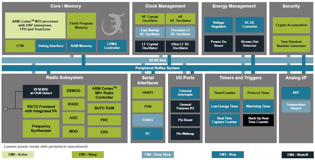
The EFR32 product family combines an energy-friendly MCU with a high performance radio transceiver. The devices are well suited for secure connected IoT multi-protocol devices requiring high performance and low energy consumption. This section gives a short intro- duction to the full radio and MCU system. The detailed functional description can be found in the EFR32xG22 Reference Manual.
A block diagram of the EFR32BG22 family is shown in Figure 3.1 Detailed EFR32BG22 Block Diagram on page 7. The diagram shows a superset of features available on the family, which vary by OPN. For more information about specific device features, consult Ordering Information. 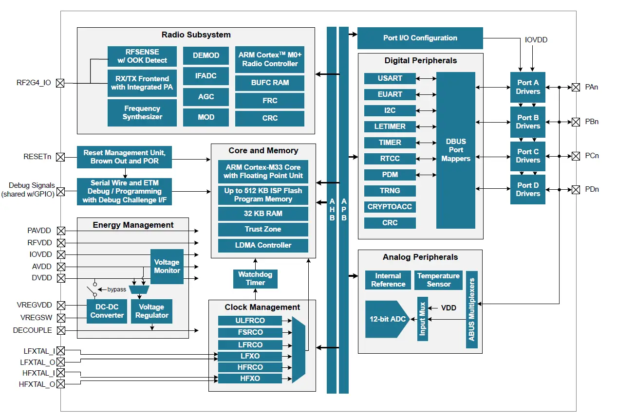
Radio
The EFR32BG22 Wireless Gecko features a highly configurable radio transceiver supporting the Bluetooth Low Energy wireless proto- col.
Antenna Interface
The 2.4 GHz antenna interface consists of a single-ended pin (RF2G4_IO). The external components for the antenna interface in typi- cal applications are shown in the RF Matching Networks section.
Fractional-N Frequency Synthesizer
The EFR32BG22 contains a high performance, low phase noise, fully integrated fractional-N frequency synthesizer. The synthesizer is used in receive mode to generate the LO frequency for the down-conversion mixer. It is also used in transmit mode to directly generate the modulated RF carrier.
The fractional-N architecture provides excellent phase noise performance, frequency resolution better than 100 Hz, and low energy consumption. The synthesizer’s fast frequency settling allows for very short receiver and transmitter wake up times to reduce system energy consumption.
Receiver Architecture
The EFR32BG22 uses a low-IF receiver architecture, consisting of a Low-Noise Amplifier (LNA) followed by an I/Q down-conversion mixer. The I/Q signals are further filtered and amplified before being sampled by the IF analog-to-digital converter (IFADC).
The IF frequency is configurable from 150 kHz to 1371 kHz. The IF can further be configured for high-side or low-side injection, providing flexibility with respect to known interferers at the image frequency.
The Automatic Gain Control (AGC) module adjusts the receiver gain to optimize performance and avoid saturation for excellent selectivity and blocking performance. The 2.4 GHz radio is calibrated at production to improve image rejection performance.
Demodulation is performed in the digital domain. The demodulator performs configurable decimation and channel filtering to allow receive bandwidths ranging from 0.1 to 2530 kHz. High carrier frequency and baud rate offsets are tolerated by active estimation and compensation. Advanced features supporting high quality communication under adverse conditions include forward error correction by block and convolutional coding as well as Direct Sequence Spread Spectrum (DSSS).
A Received Signal Strength Indicator (RSSI) is available for signal quality metrics, for level-based proximity detection, and for RF channel access by Collision Avoidance (CA) or Listen Before Talk (LBT) algorithms. An RSSI capture value is associated with each received frame and the dynamic RSSI measurement can be monitored throughout reception.
Transmitter Architecture
The EFR32BG22 uses a direct-conversion transmitter architecture. For constant envelope modulation formats, the modulator controls phase and frequency modulation in the frequency synthesizer. Transmit symbols or chips are optionally shaped by a digital shaping filter. The shaping filter is fully configurable, including the BT product, and can be used to implement Gaussian or Raised Cosine shap- ing.
Carrier Sense Multiple Access – Collision Avoidance (CSMA-CA) or Listen Before Talk (LBT) algorithms can be automatically timed by the EFR32BG22. These algorithms are typically defined by regulatory standards to improve inter-operability in a given bandwidth be- tween devices that otherwise lack synchronized RF channel access.
Packet and State Trace
The EFR32BG22 Frame Controller has a packet and state trace unit that provides valuable information during the development phase. It features:
- Non-intrusive trace of transmit data, receive data and state information
- Data observability on a single-pin UART data output, or on a two-pin SPI data output
- Configurable data output bitrate /baudrate
- Multiplexed transmitted data, received data and state / meta information in a single serial data stream
Data Buffering
The EFR32BG22 features an advanced Radio Buffer Controller (BUFC) capable of handling up to 4 buffers of adjustable size from 64 bytes to 4096 bytes. Each buffer can be used for RX, TX or both. The buffer data is located in RAM, enabling zero-copy operations.
Radio Controller (RAC)
The Radio Controller controls the top level state of the radio subsystem in the EFR32BG22. It performs the following tasks:
- Precisely-timed control of enabling and disabling of the receiver and transmitter circuitry
- Run-time calibration of receiver, transmitter and frequency synthesizer
- Detailed frame transmission timing, including optional LBT or CSMA-CA
RFSENSE Interface
The RFSENSE block allows the device to remain in EM2, EM3 or EM4 and wake when RF energy above a specified threshold is detec- ted. When operated in selective mode, the RFSENSE block performs OOK preamble and sync word detection, preventing false wake- up events.
General Purpose Input/Output (GPIO)
EFR32BG22 has up to 26 General Purpose Input/Output pins. Each GPIO pin can be individually configured as either an output or input. More advanced configurations including open-drain, open-source, and glitch-filtering can be configured for each individual GPIO pin. The GPIO pins can be overridden by peripheral connections, like SPI communication. Each peripheral connection can be routed to several GPIO pins on the device. The input value of a GPIO pin can be routed through the Peripheral Reflex System to other peripher- als. The GPIO subsystem supports asynchronous external pin interrupts.
All of the pins on ports A and port B are EM2 capable. These pins may be used by Low-Energy peripherals in EM2/3 and may also be used as EM2/3 pin wake-ups. Pins on ports C and D are latched/retained in their current state when entering EM2 until EM2 exit upon which internal peripherals could once again drive those pads.
A few GPIOs also have EM4 wake functionality. These pins are listed in the Alternate Function Table.
Clocking
Clock Management Unit (CMU)
The Clock Management Unit controls oscillators and clocks in the EFR32BG22. Individual enabling and disabling of clocks to all periph- eral modules is performed by the CMU. The CMU also controls enabling and configuration of the oscillators. A high degree of flexibility allows software to optimize energy consumption in any specific application by minimizing power dissipation in unused peripherals and oscillators.
Internal and External Oscillators
The EFR32BG22 supports two crystal oscillators and fully integrates four RC oscillators, listed below.
- A high frequency crystal oscillator (HFXO) with integrated load capacitors, tunable in small steps, provides a precise timing refer- ence for the MCU. The HFXO provides excellent RF clocking performance using a 38.4 MHz crystal. The HFXO can also support an external clock source such as a TCXO for applications that require an extremely accurate clock frequency over temperature.
- A 32.768 kHz crystal oscillator (LFXO) provides an accurate timing reference for low energy modes.
- An integrated high frequency RC oscillator (HFRCO) is available for the MCU system, when crystal accuracy is not required. The HFRCO employs fast start-up at minimal energy consumption combined with a wide frequency range, from 1 MHz to 76.8 MHz.
- An integrated fast start-up RC oscillator (FSRCO) that runs at a fixed 20 MHz
- An integrated low frequency 32.768 kHz RC oscillator (LFRCO) for low power operation without an external crystal. Precision mode enables periodic recalibration against the 38.4 MHz HFXO crystal to improve accuracy to +/- 500 ppm, suitable for BLE sleep inter- val timing.
- An integrated ultra-low frequency 1 kHz RC oscillator (ULFRCO) is available to provide a timing reference at the lowest energy con- sumption in low energy modes.
Counters/Timers and PWM
Timer/Counter (TIMER)
TIMER peripherals keep track of timing, count events, generate PWM outputs and trigger timed actions in other peripherals through the Peripheral Reflex System (PRS). The core of each TIMER is a 16-bit or 32-bit counter with up to 3 compare/capture channels. Each channel is configurable in one of three modes. In capture mode, the counter state is stored in a buffer at a selected input event. In compare mode, the channel output reflects the comparison of the counter to a programmed threshold value. In PWM mode, the TIMER supports generation of pulse-width modulation (PWM) outputs of arbitrary waveforms defined by the sequence of values written to the compare registers. In addition some timers offer dead-time insertion. See 3.13 Configuration Summary for information on the feature set of each timer.
Low Energy Timer (LETIMER)
The unique LETIMER is a 24-bit timer that is available in energy mode EM0 Active, EM1 Sleep, EM2 Deep Sleep, and EM3 Stop. This allows it to be used for timing and output generation when most of the device is powered down, allowing simple tasks to be performed while the power consumption of the system is kept at an absolute minimum. The LETIMER can be used to output a variety of wave- forms with minimal software intervention. The LETIMER is connected to the Peripheral Reflex System (PRS), and can be configured to start counting on compare matches from other peripherals such as the RTCC.
Real Time Clock with Capture (RTCC)
The Real Time Clock with Capture (RTCC) is a 32-bit counter providing timekeeping down to EM3. The RTCC can be clocked by any of the on-board low-frequency oscillators, and it is capable of providing system wake-up at user defined intervals.
A secondary RTC is used by the RF protocol stack for event scheduling, leaving the primary RTCC block available exclusively for appli- cation software.
Back-Up Real Time Counter
The Back-Up Real Time Counter (BURTC) is a 32-bit counter providing timekeeping in all energy modes, including EM4. The BURTC can be clocked by any of the on-board low-frequency oscillators, and it is capable of providing system wake-up at user defined invervals.
Watchdog Timer (WDOG)
The watchdog timer can act both as an independent watchdog or as a watchdog synchronous with the CPU clock. It has windowed monitoring capabilities, and can generate a reset or different interrupts depending on the failure mode of the system. The watchdog can also monitor autonomous systems driven by the Peripheral Reflex System (PRS).
Communications and Other Digital Peripherals
Universal Synchronous/Asynchronous Receiver/Transmitter (USART)
The Universal Synchronous/Asynchronous Receiver/Transmitter is a flexible serial I/O module. It supports full duplex asynchronous UART communication with hardware flow control as well as RS-485, SPI, MicroWire and 3-wire. It can also interface with devices sup- porting:
- ISO7816 SmartCards
- IrDA
- I2S
Enhanced Universal Asynchronous Receiver/Transmitter (EUART)
The Enhanced Universal Asynchronous Receiver/Transmitter supports full duplex asynchronous UART communication with hardware flow control, RS-485 and IrDA support. In EM0 and EM1 the EUART provides a high-speed, buffered communication interface. When routed to GPIO ports A or B, the EUART may also be used in a low-energy mode and operate in EM2. A 32.768 kHz clock source allows full duplex UART communication up to 9600 baud.
Inter-Integrated Circuit Interface (I2C)
The I2C module provides an interface between the MCU and a serial I2C bus. It is capable of acting as both a master and a slave and supports multi-master buses. Standard-mode, fast-mode and fast-mode plus speeds are supported, allowing transmission rates from 10 kbit/s up to 1 Mbit/s. Slave arbitration and timeouts are also available, allowing implementation of an SMBus-compliant system. The interface provided to software by the I2C module allows precise timing control of the transmission process and highly automated trans- fers. Automatic recognition of slave addresses is provided in active and low energy modes. Note that not all instances of I2C are avalia- ble in all energy modes.
Peripheral Reflex System (PRS)
The Peripheral Reflex System provides a communication network between different peripheral modules without software involvement. Peripheral modules producing Reflex signals are called producers. The PRS routes Reflex signals from producers to consumer periph- erals which in turn perform actions in response. Edge triggers and other functionality such as simple logic operations (AND, OR, NOT) can be applied by the PRS to the signals. The PRS allows peripherals to act autonomously without waking the MCU core, saving power.
Pulse Density Modulation (PDM) Interface
The PDM module provides a serial interface and decimation filter for Pulse Density Modulation (PDM) microphones, isolated Sigma- delta ADCs, digital sensors and other PDM or sigma delta bit stream peripherals. A programmable Cascaded Integrator Comb (CIC) filter is used to decimate the incoming bit streams. PDM supports stereo or mono input data and DMA transfer.
Security Features
The following security features are available on the EFR32BG22:
- Secure Boot with Root of Trust and Secure Loader (RTSL)
- Cryptographic Accelerator
- True Random Number Generator (TRNG)
- Secure Debug with Lock/Unlock
Secure Boot with Root of Trust and Secure Loader (RTSL)
The Secure Boot with RTSL authenticates a chain of trusted firmware that begins from an immutable memory (ROM).
It prevents malware injection, prevents rollback, ensures that only authentic firmware is executed and protects Over The Air updates. More information on this feature can be found in the Application Note AN1218: Series 2 Secure Boot with RTSL.
Cryptographic Accelerator
The Cryptographic Accelerator is an autonomous hardware accelerator which supports AES encryption and decryption with 128/192/256-bit keys, Elliptic Curve Cryptography (ECC) to support public key operations and hashes. Supported block cipher modes of operation for AES include:
- ECB (Electronic Code Book)
- CTR (Counter Mode)
- CBC (Cipher Block Chaining)
- CFB (Cipher Feedback)
- GCM (Galois Counter Mode)
- CBC-MAC (Cipher Block Chaining Message Authentication Code)
- GMAC (Galois Message Authentication Code)
- CCM (Counter with CBC-MAC)
The Cryptographic Accelerator accelerates Elliptical Curve Cryptography and supports the NIST (National Institute of Standards and Technology) recommended curves including P-192 and P-256 for ECDH(Elliptic Curve Diffie-Hellman) key derivation and ECDSA (El- liptic Curve Digital Signature Algorithm) sign and verify operations.
Supported hashes include SHA-1, SHA2/224, and SHA-2/256.
This implementation provides a fast and energy efficient solution to state of the art cryptographic needs.
True Random Number Generator
The True Random Number Generator module is a non-deterministic random number generator that harvests entropy from a thermal energy source. It includes start-up health tests for the entropy source as required by NIST SP800-90B and AIS-31 as well as online health tests required for NIST SP800-90C.
The TRNG is suitable for periodically generating entropy to seed an approved pseudo random number generator.
Secure Debug with Lock/Unlock
For obvious security reasons, it is critical for a product to have its debug interface locked before being released in the field.
In addition, the EFR32BG22 also provides a secure debug unlock function that allows authenticated access based on public key cryp- tography. This functionality is particularly useful for supporting failure analysis while maintaining confidentiality of IP and sensitive end- user data.
More information on this feature can be found in the Application Note AN1190: EFR32xG2x Secure Debug.
Analog
Analog to Digital Converter (IADC)
The IADC is a hybrid architecture combining techniques from both SAR and Delta-Sigma style converters. It has a resolution of 12 bits at 1 Msps and 16 bits at up to 76.9 ksps. Hardware oversampling reduces system-level noise over multiple front-end samples. The IADC includes integrated voltage reference options. Inputs are selectable from a wide range of sources, including pins configurable as either single-ended or differential.
Power
The EFR32BG22 has an Energy Management Unit (EMU) and efficient integrated regulators to generate internal supply voltages. Only a single external supply voltage is required, from which all internal voltages are created. An optional integrated DC-DC buck regulator can be utilized to further reduce the current consumption. The DC-DC regulator requires one external inductor and one external capaci- tor.
The EFR32BG22 device family includes support for internal supply voltage scaling, as well as two different power domains groups for peripherals. These enhancements allow for further supply current reductions and lower overall power consumption.
Energy Management Unit (EMU)
The Energy Management Unit manages transitions of energy modes in the device. Each energy mode defines which peripherals and features are available and the amount of current the device consumes. The EMU can also be used to implement system-wide voltage scaling and turn off the power to unused RAM blocks to optimize the energy consumption in the target application. The DC-DC regula- tor operation is tightly integrated with the EMU.
Voltage Scaling
The EFR32BG22 supports supply voltage scaling for the LDO powering DECOUPLE, with independent selections for EM0 / EM1 and EM2 / EM3. Voltage scaling helps to optimize the energy efficiency of the system by operating at lower voltages when possible. The default EM0 / EM1 voltage scaling level is VSCALE2, which allows the core to operate in active mode at full speed. The intermediate level, VSCALE1, allows operation in EM0 and EM1 at up to 40 MHz. The lowest level, VSCALE0, can be used to conserve power in EM2 and EM3. The EMU will automatically switch the target voltage scaling level when transitioning between energy modes.
DC-DC Converter
The DC-DC buck converter covers a wide range of load currents, provides high efficiency in energy modes EM0, EM1, EM2 and EM3, and can supply up to 60 mA for device and radio operation. RF noise mitigation allows operation of the DC-DC converter without significantly degrading sensitivity of radio components. An on-chip supply-monitor signals when the supply voltage is low to allow bypass of the regulator via programmable software interrupt. It employs soft switching at boot and DCDC regulating-to-bypass transitions to limit the max supply slew-rate and mitigate inrush current.
Power Domains
The EFR32BG22 has three peripheral power domains for operation in EM2 and EM3, as well as the ability to selectively retain configu- rations for EM0/EM1 peripherals. A small set of peripherals always remain powered on in EM2 and EM3, including all peripherals which are available in EM4. If all of the peripherals in PD0B or PD0C are configured as unused, that power domain will be powered off in EM2 or EM3, reducing the overall current consumption of the device. Likewise, if the application can tolerate the setup time to re-configure used EM0/EM1 peripherals on wake, register retention for these peripherals can be disabled to further reduce the EM2 or EM3 current.
Peripheral Power Subdomains
| Always available in EM2/EM3 | Power Domain PD0B | Power Domain PD0C |
| RTCC | LETIMER0 | LFRCO (Precision Mode) |
| LFRCO (Non-precision mode)1 | IADC0 | |
| LFXO1 | I2C0 | |
| BURTC1 | WDOG0 | |
| RFSENSE1 | EUART0 | |
| ULFRCO1 | PRS | |
| FSRCO | DEBUG | |
| Note: 1. Peripheral also available in EM4. | ||
Reset Management Unit (RMU)
The RMU is responsible for handling reset of the EFR32BG22. A wide range of reset sources are available, including several power supply monitors, pin reset, software controlled reset, core lockup reset, and watchdog reset.
Core and Memory
Processor Core
The ARM Cortex-M processor includes a 32-bit RISC processor integrating the following features and tasks in the system:
- ARM Cortex-M33 RISC processor achieving 1.50 Dhrystone MIPS/MHz
- ARM TrustZone security technology
- Embedded Trace Macrocell (ETM) for real-time trace and debug
- Up to 512 kB flash program memory
- Up to 32 kB RAM data memory
- Configuration and event handling of all modules
- 2-pin Serial-Wire debug interface
Memory System Controller (MSC)
The Memory System Controller (MSC) is the program memory unit of the microcontroller. The flash memory is readable and writable from both the Cortex-M and DMA. In addition to the main flash array where Program code is normally written the MSC also provides an Information block where additional information such as special user information or flash-lock bits are stored. There is also a read-only page in the information block containing system and device calibration data. Read and write operations are supported in energy modes EM0 Active and EM1 Sleep.
Linked Direct Memory Access Controller (LDMA)
The Linked Direct Memory Access (LDMA) controller allows the system to perform memory operations independently of software. This reduces both energy consumption and software workload. The LDMA allows operations to be linked together and staged, enabling sophisticated operations to be implemented.
Memory Map
The EFR32BG22 memory map is shown in the figures below. RAM and flash sizes are for the largest memory configuration. 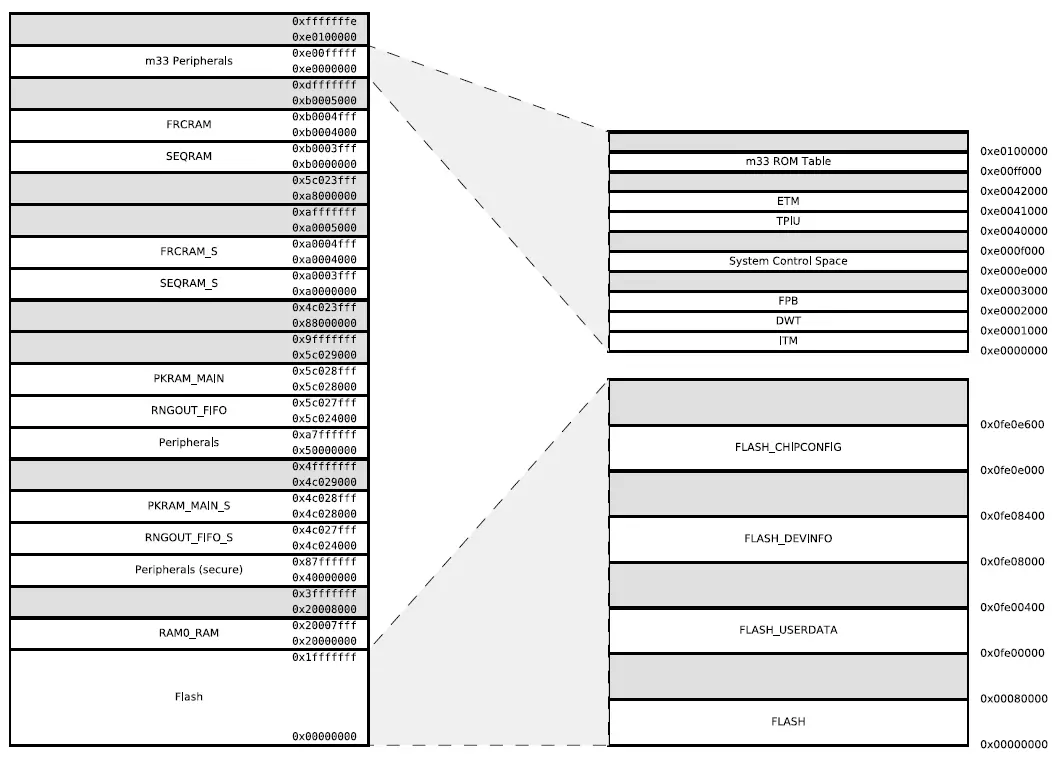
Configuration Summary
The features of the EFR32BG22 are a subset of the feature set described in the device reference manual. The table below describes device specific implementation of the features. Remaining modules support full configuration.
Configuration Summary
| Module | Lowest Energy Mode | Configuration |
| I2C0 | EM21 | |
| I2C1 | EM1 | |
| IADC0 | EM2 | |
| LETIMER0 | EM21 | |
| PDM | EM1 | 2-channel |
| TIMER0 | EM1 | 32-bit, 3-channels, +DTI |
| TIMER1 | EM1 | 16-bit, 3-channels, +DTI |
| TIMER2 | EM1 | 16-bit, 3-channels, +DTI |
| TIMER3 | EM1 | 16-bit, 3-channels, +DTI |
| TIMER4 | EM1 | 16-bit, 3-channels, +DTI |
| EUART0 | EM1 – Full high-speed operation EM21 – Low-energy operation, 9600 Baud | |
| USART0 | EM1 | +IrDA, +I2S, +SmartCard |
| USART1 | EM1 | +IrDA, +I2S, +SmartCard |
| Note: 1. EM2 and EM3 operation is only supported for digital peripheral I/O on Port A and Port B. All GPIO ports support digital peripheral operation in EM0 and EM1. | ||
Electrical Specifications
Electrical Characteristics
All electrical parameters in all tables are specified under the following conditions, unless stated otherwise:
- Typical values are based on TA=25 °C and all supplies at 3.0 V, by production test and/or technology characterization.
- Radio performance numbers are measured in conducted mode, based on Silicon Laboratories reference designs using output pow- er-specific external RF impedance-matching networks for interfacing to a 50 Ω antenna.
- Minimum and maximum values represent the worst conditions across supply voltage, process variation, and operating temperature, unless stated otherwise.
Power Supply Pin Dependencies
Due to on-chip circuitry (e.g., diodes), some EFR32 power supply pins have a dependent relationship with one or more other power supply pins. These internal relationships between the external voltages applied to the various EFR32 supply pins are defined below. Exceeding the below constraints can result in damage to the device and/or increased current draw.
- VREGVDD & DVDD
- In systems using the DCDC converter, DVDD (the buck converter output) should be connected to the recommended LDCDC and CDCDC, and should not be driven by an off-chip regulator.
- In systems not using the DCDC converter, DVDD must be shorted to VREGVDD on the PCB (VREGVDD=DVDD)
- DVDD ≥ DECOUPLE
- PAVDD ≥ RFVDD
- AVDD, IOVDD: No dependency with each other or any other supply pin
Absolute Maximum Ratings
Stresses beyond those listed below may cause permanent damage to the device. This is a stress rating only and functional operation of the devices at those or any other conditions beyond those indicated in the operation listings of this specification is not implied. Exposure to maximum rating conditions for extended periods may affect device reliability. For more information on the available quality and relia- bility data, see the Quality and Reliability Monitor Report at http://www.silabs.com/support/quality/pages/default.aspx.
Absolute Maximum Ratings
| Parameter | Symbol | Test Condition | Min | Typ | Max | Unit |
| Storage temperature range | TSTG | -50 | — | +150 | °C | |
| Voltage on any supply pin1 | VDDMAX | -0.3 | — | 3.8 | V | |
| Junction temperature | TJMAX | -G grade | — | — | +105 | °C |
| -I grade | — | — | +125 | °C | ||
| Voltage ramp rate on any supply pin | VDDRAMPMAX | — | — | 1.0 | V / µs | |
| Voltage on HFXO pins | VHFXOPIN | -0.3 | — | 1.4 | V | |
| DC voltage on any GPIO pin | VDIGPIN | -0.3 | — | VIOVDD + 0.3 | V | |
| DC voltage on RESETn pin2 | VRESETn | -0.3 | — | 3.8 | V | |
| Input RF level on RF pins RF2G4_IO | PRFMAX2G4 | — | — | +10 | dBm | |
| Absolute voltage on RF pin RF2G4_IO | VMAX2G4 | -0.3 | — | VPAVDD + 0.3 | V | |
| Total current into VDD power lines | IVDDMAX | Source | — | — | 200 | mA |
| Total current into VSS ground lines | IVSSMAX | Sink | — | — | 200 | mA |
| Current per I/O pin | IIOMAX | Sink | — | — | 50 | mA |
| Source | — | — | 50 | mA | ||
| Current for all I/O pins | IIOALLMAX | Sink | — | — | 200 | mA |
| Source | — | — | 200 | mA | ||
Note:
| ||||||
General Operating Conditions
Table 4.2. General Operating Conditions
| Parameter | Symbol | Test Condition | Min | Typ | Max | Unit |
| Operating ambient tempera- ture range | TA | -G temperature grade 1 | -40 | — | +85 | °C |
| -I temperature grade 1 | -40 | — | +125 | ° C | ||
| DVDD supply voltage | VDVDD | EM0/1 | 1.71 | 3.0 | 3.8 | V |
| EM2/3/42 | 1.71 | 3.0 | 3.8 | V | ||
| AVDD supply voltage | VAVDD | 1.71 | 3.0 | 3.8 | V | |
| IOVDDx operating supply voltage (All IOVDD pins) | VIOVDDx | 1.71 | 3.0 | 3.8 | V | |
| PAVDD operating supply voltage | VPAVDD | 1.71 | 3.0 | 3.8 | V | |
| VREGVDD operating supply voltage | VVREGVDD | DC-DC in regulation3 | 2.2 | 3.0 | 3.8 | V |
| DC-DC in bypass 60 mA load | 1.8 | 3.0 | 3.8 | V | ||
| DC-DC not in use. DVDD exter- nally shorted to VREGVDD | 1.71 | 3.0 | 3.8 | V | ||
| RFVDD operating supply voltage | VRFVDD | 1.71 | 3.0 | VPAVDD | V | |
| DECOUPLE output capaci- tor4 | CDECOUPLE | 1.0 µF ± 10% X8L capacitor used for performance characterization. | 1.0 | — | 2.75 | µF |
| HCLK and SYSCLK frequen- cy | fHCLK | VSCALE2, MODE = WS1 | — | — | 76.8 | MHz |
| VSCALE2, MODE = WS0 | — | — | 40 | MHz | ||
| VSCALE1, MODE = WS0 | — | — | 40 | MHz | ||
| PCLK frequency | fPCLK | VSCALE2 | — | — | 50 | MHz |
| VSCALE1 | — | — | 40 | MHz | ||
| EM01 Group A clock fre- quency | fEM01GRPACLK | VSCALE2 | — | — | 76.8 | MHz |
| VSCALE1 | — | — | 40 | MHz | ||
| EM01 Group B clock fre- quency | fEM01GRPBCLK | VSCALE2 | — | — | 76.8 | MHz |
| VSCALE1 | — | — | 40 | MHz | ||
| Radio HCLK frequency5 | fRHCLK | VSCALE2 or VSCALE1 | — | 38.4 | — | MHz |
| Parameter | Symbol | Test Condition | Min | Typ | Max | Unit |
Note:
| ||||||
DC-DC Converter
Test conditions: LDCDC = 2.2 µH (Samsung CIG22H2R2MNE), CDCDC = 4.7 µF (Samsung CL10B475KQ8NQNC), VVREGVDD = 3.0 V,
VOUT = 1.8 V, IPKVAL in EM0/1 modes is set to 150 mA, and in EM2/3 modes is set to 90 mA, unless otherwise indicated.
Table 4.3. DC-DC Converter
| Parameter | Symbol | Test Condition | Min | Typ | Max | Unit |
| Input voltage range at VREGVDD pin1 | VVREGVDD | DCDC in regulation, ILOAD = 60 mA, EM0/EM1 mode | 2.2 | 3.0 | 3.8* | V |
| DCDC in regulation, ILOAD = 5 mA, EM0/EM1 or EM2/EM3 mode | 1.8 | 3.0 | 3.8* | V | ||
| Bypass mode | 1.8 | 3.0 | 3.8 | V | ||
| Regulated output voltage | VOUT | — | 1.8 | — | V | |
| Regulation DC accuracy | ACCDC | VVREGVDD ≥ 2.2 V, Steady state in EM0/EM1 mode or EM2/EM3 mode | -2.5 | — | 3.3 | % |
| Regulation total accuracy | ACCTOT | With mode transitions between EM0/EM1 and EM2/EM3 modes | -5 | — | 7 | % |
| Steady-state output ripple | VR | ILOAD = 20 mA in EM0/EM1 mode | — | 14.3 | — | mVpp |
| DC line regulation | VREG | ILOAD = 60 mA in EM0/EM1 mode, VVREGVDD ≥ 2.2 V | — | 5.5 | — | mV/V |
| DC load regulation | IREG | Load current between 100 µA and 60 mA in EM0/EM1 mode | — | 0.27 | — | mV/mA |
| Efficiency | EFF | Load current between 100 µA and 60 mA in EM0/EM1 mode, or be- tween 10 µA and 5 mA in EM2/EM3 mode | — | 91 | — | % |
| Output load current | ILOAD | EM0/EM1 mode, DCDC in regulation | — | — | 60 | mA |
| EM2/EM3 mode, DCDC in regulation | — | — | 5 | mA | ||
| Bypass mode | — | — | 60 | mA | ||
| Nominal output capacitor | CDCDC | 4.7 µF ± 10% X7R capacitor used for performance characterization2 | 4.7 | — | 10 | µF |
| Nominal inductor | LDCDC | ± 20% tolerance | — | 2.2 | — | µH |
| Nominal input capacitor | CIN | CDCDC | — | — | µF | |
| Resistance in bypass mode | RBYP | Bypass switch from VREGVDD to DVDD, VVREGVDD = 1.8 V | — | 1.75 | 3 | Ω |
| Powertrain PFET switch from VREGVDD to VREGSW, VVREGVDD = 1.8 V | — | 0.86 | 1.5 | Ω | ||
| Supply monitor threshold programming range | VCMP_RNG | Programmable in 0.1 V steps | 2.0 | — | 2.3 | V |
| Supply monitor threshold ac- curacy | VCMP_ACC | Supply falling edge trip point | -5 | — | 5 | % |
| Parameter | Symbol | Test Condition | Min | Typ | Max | Unit |
| Supply monitor threshold hysteresis | VCMP_HYST | Positive hysteresis on the supply rising edge referred to the falling edge trip point | — | 4 | — | % |
| Supply monitor response time | tCMP_DELAY | Supply falling edge at -100 mV / µs | — | 0.6 | — | µs |
Note:
| ||||||
DC-DC Operating Limits
The maximum supported voltage on the VREGVDD supply pin is limited under certain conditions. Maximum input voltage is a function of temperature and the average load current over a 10-year lifetime. Figure 4.1 Lifetime average load current limit vs. Maximum input voltage on page 23 shows the safe operating region under specific conditions. Exceeding this safe operating range may impact the reliability and performance of the DC-DC converter.
The average load current for an application can typically be determined by examining the current profile during the time the device is powered. For example, an application that is continuously powered which spends 99% of the time asleep consuming 2 µA and 1% of the time active and consuming 10 mA has an average lifetime load current of about 102 µA.
Figure 4.1. Lifetime average load current limit vs. Maximum input voltage
The minimum input voltage for the DC-DC in EM0/EM1 mode is a function of the maximum load current, and the peak current setting. Figure 4.2 Transient maximum load current vs. Minimum input voltage on page 23 shows the max load current vs. input voltage for different DC-DC peak inductor current settings.
Thermal Characteristics
Table 4.4. Thermal Characteristics
| Parameter | Symbol | Test Condition | Min | Typ | Max | Unit |
| Thermal Resistance Junction to Ambient QFN32 (4x4mm) Package | THE- TAJA_QFN32_4X4 | 4-Layer PCB, Natural Convection1 | — | 35.4 | — | °C/W |
| Thermal Resistance Junction to Ambient TQFN32 (4x4mm) Package | THE- TAJA_TQFN32_4X 4 | 4-Layer PCB, Natural Convection1 | — | 40.2 | — | °C/W |
| Thermal Resistance, Junc- tion to Ambient, QFN40 (5x5mm) Package | THE- TAJA_QFN40_5X5 | 4-Layer PCB, Natural Convection1 | — | 32.6 | — | °C/W |
| Note: 1. Measured according to JEDEC standard JESD51-2A. Integrated Circuit Thermal Test Method Environmental Conditions – Natural Convection (Still Air). | ||||||
Current Consumption
MCU current consumption using DC-DC at 3.0 V input
Unless otherwise indicated, typical conditions are: VREGVDD = 3.0 V. AVDD = DVDD = IOVDD = RFVDD = PAVDD = 1.8 V from DC- DC. Voltage scaling level = VSCALE1. TA = 25 °C. Minimum and maximum values in this table represent the worst conditions across process variation at TA = 25 °C.
Table 4.5. MCU current consumption using DC-DC at 3.0 V input
| Parameter | Symbol | Test Condition | Min | Typ | Max | Unit |
| Current consumption in EM0 mode with all peripherals dis- abled | IACTIVE | 76.8 MHz HFRCO w/ DPLL refer- enced to 38.4 MHz crystal, CPU running Prime from flash, VSCALE2 | — | 28 | — | µA/MHz |
| 76.8 MHz HFRCO w/ DPLL refer- enced to 38.4 MHz crystal, CPU running while loop from flash, VSCALE2 | — | 27 | — | µA/MHz | ||
| 76.8 MHz HFRCO w/ DPLL refer- enced to 38.4 MHz crystal, CPU running CoreMark loop from flash, VSCALE2 | — | 37 | — | µA/MHz | ||
| 38.4 MHz crystal, CPU running Prime from flash | — | 28 | — | µA/MHz | ||
| 38.4 MHz crystal, CPU running while loop from flash | — | 26 | — | µA/MHz | ||
| 38.4 MHz crystal, CPU running CoreMark loop from flash | — | 38 | — | µA/MHz | ||
| 38 MHz HFRCO, CPU running while loop from flash | — | 22 | — | µA/MHz | ||
| 26 MHz HFRCO, CPU running while loop from flash | — | 24 | — | µA/MHz | ||
| 16 MHz HFRCO, CPU running while loop from flash | — | 27 | — | µA/MHz | ||
| 1 MHz HFRCO, CPU running while loop from flash | — | 159 | — | µA/MHz | ||
| Current consumption in EM1 mode with all peripherals dis- abled | IEM1 | 76.8 MHz HFRCO w/ DPLL refer- enced to 38.4 MHz crystal, VSCALE2 | — | 17 | — | µA/MHz |
| 38.4 MHz crystal | — | 17 | — | µA/MHz | ||
| 38 MHz HFRCO | — | 13 | — | µA/MHz | ||
| 26 MHz HFRCO | — | 15 | — | µA/MHz | ||
| 16 MHz HFRCO | — | 18 | — | µA/MHz | ||
| 1 MHz HFRCO | — | 150 | — | µA/MHz |
| Parameter | Symbol | Test Condition | Min | Typ | Max | Unit |
| Current consumption in EM2 mode, VSCALE0 | IEM2_VS | Full RAM retention and RTC run- ning from LFXO | — | 1.40 | — | µA |
| Full RAM retention and RTC run- ning from LFRCO | — | 1.40 | — | µA | ||
| Full RAM retention and RTC run- ning from LFRCO in precision mode | — | 1.75 | — | µA | ||
| 24 kB RAM retention and RTC running from LFXO | — | 1.32 | — | µA | ||
| 24 kB RAM retention and RTC running from LFRCO in precision mode | — | 1.66 | — | µA | ||
| 8 kB RAM retention and RTC run- ning from LFXO | — | 1.21 | — | µA | ||
| 8 kB RAM retention and RTC run- ning from LFRCO | — | 1.20 | — | µA | ||
| 8 kB RAM retention and RTC run- ning from LFXO, Radio RAM and CPU cache not retained | — | 1.03 | — | µA | ||
| Current consumption in EM3 mode, VSCALE0 | IEM3_VS | 8 kB RAM retention and RTC run- ning from ULFRCO | — | 1.05 | — | µA |
| Additional current in EM2 or EM3 when any peripheral in PD0B is enabled1 | IPD0B_VS | — | 0.37 | — | µA | |
| Note: 1. Extra current consumed by power domain. Does not include current associated with the enabled peripherals. See for a list of the peripherals in each power domain. | ||||||
MCU current consumption at 3.0 V
Unless otherwise indicated, typical conditions are: AVDD = DVDD = RFVDD = PAVDD = VREGVDD = 3.0 V. DC-DC not used. Voltage scaling level = VSCALE1. TA = 25 °C. Minimum and maximum values in this table represent the worst conditions across process variation at TA = 25 °C.
| Parameter | Symbol | Test Condition | Min | Typ | Max | Unit |
| Current consumption in EM0 mode with all peripherals dis- abled | IACTIVE | 76.8 MHz HFRCO w/ DPLL refer- enced to 38.4 MHz crystal, CPU running Prime from flash, VSCALE2 | — | 42 | — | µA/MHz |
| 76.8 MHz HFRCO w/ DPLL refer- enced to 38.4 MHz crystal, CPU running while loop from flash, VSCALE2 | — | 39 | — | µA/MHz | ||
| 76.8 MHz HFRCO w/ DPLL refer- enced to 38.4 MHz crystal, CPU running CoreMark loop from flash, VSCALE2 | — | 54 | — | µA/MHz | ||
| 38.4 MHz crystal, CPU running Prime from flash | — | 40 | — | µA/MHz | ||
| 38.4 MHz crystal, CPU running while loop from flash | — | 39 | — | µA/MHz | ||
| 38.4 MHz crystal, CPU running CoreMark loop from flash | — | 55 | — | µA/MHz | ||
| 38 MHz HFRCO, CPU running while loop from flash | — | 33 | 50 | µA/MHz | ||
| 26 MHz HFRCO, CPU running while loop from flash | — | 35 | — | µA/MHz | ||
| 16 MHz HFRCO, CPU running while loop from flash | — | 40 | — | µA/MHz | ||
| 1 MHz HFRCO, CPU running while loop from flash | — | 228 | 830 | µA/MHz | ||
| Current consumption in EM1 mode with all peripherals dis- abled | IEM1 | 76.8 MHz HFRCO w/ DPLL refer- enced to 38.4 MHz crystal, VSCALE2 | — | 24 | — | µA/MHz |
| 38.4 MHz crystal | — | 25 | — | µA/MHz | ||
| 38 MHz HFRCO | — | 19 | 35 | µA/MHz | ||
| 26 MHz HFRCO | — | 21 | — | µA/MHz | ||
| 16 MHz HFRCO | — | 27 | — | µA/MHz | ||
| 1 MHz HFRCO | — | 215 | 770 | µA/MHz |
| Parameter | Symbol | Test Condition | Min | Typ | Max | Unit |
| Current consumption in EM2 mode, VSCALE0 | IEM2_VS | Full RAM retention and RTC run- ning from LFXO | — | 1.94 | — | µA |
| Full RAM retention and RTC run- ning from LFRCO | — | 1.95 | 4.9 | µA | ||
| 24 kB RAM retention and RTC running from LFXO | — | 1.81 | — | µA | ||
| 24 kB RAM retention and RTC running from LFRCO in precision mode | — | 2.34 | — | µA | ||
| 8 kB RAM retention and RTC run- ning from LFXO | — | 1.64 | — | µA | ||
| 8 kB RAM retention and RTC run- ning from LFRCO | — | 1.65 | — | µA | ||
| 8 kB RAM retention and RTC run- ning from LFXO, Radio RAM and CPU cache not retained | — | 1.39 | — | µA | ||
| Current consumption in EM3 mode, VSCALE0 | IEM3_VS | 8 kB RAM retention and RTC run- ning from ULFRCO | — | 1.41 | 3.7 | µA |
| Current consumption in EM4 mode | IEM4 | No BURTC, no LF oscillator | — | 0.17 | 0.43 | µA |
| BURTC with LFXO | — | 0.50 | — | µA | ||
| Current consumption during reset | IRST | Hard pin reset held | — | 234 | — | µA |
| Additional current in EM2 or EM3 when any peripheral in PD0B is enabled1 | IPD0B_VS | — | 0.56 | — | µA | |
| Note: 1. Extra current consumed by power domain. Does not include current associated with the enabled peripherals. See for a list of the peripherals in each power domain. | ||||||
MCU current consumption at 1.8 V
Unless otherwise indicated, typical conditions are: AVDD = DVDD = RFVDD = PAVDD = VREGVDD = 1.8 V. DC-DC not used. Voltage scaling level = VSCALE1. TA = 25 °C. Minimum and maximum values in this table represent the worst conditions across process variation at TA = 25 °C.
MCU current consumption at 1.8 V
| Parameter | Symbol | Test Condition | Min | Typ | Max | Unit |
| Current consumption in EM0 mode with all peripherals dis- abled | IACTIVE | 76.8 MHz HFRCO w/ DPLL refer- enced to 38.4 MHz crystal, CPU running Prime from flash, VSCALE2 | — | 42 | — | µA/MHz |
| 76.8 MHz HFRCO w/ DPLL refer- enced to 38.4 MHz crystal, CPU running while loop from flash, VSCALE2 | — | 39 | — | µA/MHz | ||
| 76.8 MHz HFRCO w/ DPLL refer- enced to 38.4 MHz crystal, CPU running CoreMark loop from flash, VSCALE2 | — | 54 | — | µA/MHz | ||
| 38.4 MHz crystal, CPU running Prime from flash | — | 41 | — | µA/MHz | ||
| 38.4 MHz crystal, CPU running while loop from flash | — | 39 | — | µA/MHz | ||
| 38.4 MHz crystal, CPU running CoreMark loop from flash | — | 55 | — | µA/MHz | ||
| 38 MHz HFRCO, CPU running while loop from flash | — | 33 | — | µA/MHz | ||
| 26 MHz HFRCO, CPU running while loop from flash | — | 35 | — | µA/MHz | ||
| 16 MHz HFRCO, CPU running while loop from flash | — | 40 | — | µA/MHz | ||
| 1 MHz HFRCO, CPU running while loop from flash | — | 227 | — | µA/MHz | ||
| Current consumption in EM1 mode with all peripherals dis- abled | IEM1 | 76.8 MHz HFRCO w/ DPLL refer- enced to 38.4 MHz crystal, VSCALE2 | — | 24 | — | µA/MHz |
| 38.4 MHz crystal | — | 25 | — | µA/MHz | ||
| 38 MHz HFRCO | — | 19 | — | µA/MHz | ||
| 26 MHz HFRCO | — | 21 | — | µA/MHz | ||
| 16 MHz HFRCO | — | 27 | — | µA/MHz | ||
| 1 MHz HFRCO | — | 213 | — | µA/MHz |
| Parameter | Symbol | Test Condition | Min | Typ | Max | Unit |
| Current consumption in EM2 mode, VSCALE0 | IEM2_VS | Full RAM retention and RTC running from LFXO | — | 1.87 | — | µA |
| Full RAM retention and RTC running from LFRCO | — | 1.86 | — | µA | ||
| 24 kB RAM retention and RTC running from LFXO | — | 1.73 | — | µA | ||
| 24 kB RAM retention and RTC running from LFRCO in precision mode | — | 2.26 | — | µA | ||
| 8 kB RAM retention and RTC running from LFXO | — | 1.57 | — | µA | ||
| 8 kB RAM retention and RTC running from LFRCO | — | 1.56 | — | µA | ||
| 8 kB RAM retention and RTC running from LFXO, Radio RAM and CPU cache not retained | — | 1.32 | — | µA | ||
| Current consumption in EM3 mode, VSCALE0 | IEM3_VS | 8 kB RAM retention and RTC running from ULFRCO | — | 1.34 | — | µA |
| Current consumption in EM4 mode | IEM4 | No BURTC, no LF oscillator | — | 0.13 | — | µA |
| BURTC with LFXO | — | 0.44 | — | µA | ||
| Current consumption during reset | IRST | Hard pin reset held | — | 190 | — | µA |
| Additional current in EM2 or EM3 when any peripheral in PD0B is enabled1 | IPD0B_VS | — | 0.54 | — | µA | |
| Note: 1. Extra current consumed by power domain. Does not include current associated with the enabled peripherals. See for a list of the peripherals in each power domain. | ||||||
Radio current consumption at 3.0V using DCDC
RF current consumption measured with MCU in EM1, HCLK = 38.4 MHz, and all MCU peripherals disabled. Unless otherwise indica- ted, typical conditions are: VREGVDD = 3.0V. AVDD = DVDD = IOVDD = RFVDD = PAVDD = 1.8 V powered from DCDC. TA = 25 °C. Minimum and maximum values in this table represent the worst conditions across process variation at TA = 25 °C.
Radio current consumption at 3.0V using DCDC
| Parameter | Symbol | Test Condition | Min | Typ | Max | Unit |
| System current consumption in receive mode, active pack- et reception | IRX_ACTIVE | 125 kbit/s, 2GFSK, f = 2.4 GHz, VSCALE1, EM1P (Radio clocks only) | — | 3.7 | — | mA |
| 125 kbit/s, 2GFSK, f = 2.4 GHz, VSCALE1 | — | 4.0 | — | mA | ||
| 125 kbit/s, 2GFSK, f = 2.4 GHz, VSCALE2 | — | 4.1 | — | mA | ||
| 500 kbit/s, 2GFSK, f = 2.4 GHz, VSCALE1, EM1P (Radio clocks only) | — | 3.8 | — | mA | ||
| 500 kbit/s, 2GFSK, f = 2.4 GHz, VSCALE1 | — | 4.0 | — | mA | ||
| 500 kbit/s, 2GFSK, f = 2.4 GHz, VSCALE2 | — | 4.2 | — | mA | ||
| 1 Mbit/s, 2GFSK, f = 2.4 GHz, VSCALE1, EM1P (Radio clocks only) | — | 3.6 | — | mA | ||
| 1 Mbit/s, 2GFSK, f = 2.4 GHz, VSCALE1 | — | 3.8 | — | mA | ||
| 1 Mbit/s, 2GFSK, f = 2.4 GHz, VSCALE2 | — | 3.9 | — | mA | ||
| 2 Mbit/s, 2GFSK, f = 2.4 GHz, VSCALE1, EM1P (Radio clocks only) | — | 4.0 | — | mA | ||
| 2 Mbit/s, 2GFSK, f = 2.4 GHz, VSCALE1 | — | 4.2 | — | mA | ||
| 2 Mbit/s, 2GFSK, f = 2.4 GHz, VSCALE2 | — | 4.4 | — | mA |
| Parameter | Symbol | Test Condition | Min | Typ | Max | Unit |
| System current consumption in receive mode, listening for packet | IRX_LISTEN | 125 kbit/s, 2GFSK, f = 2.4 GHz, VSCALE1, EM1P (Radio clocks only) | — | 3.8 | — | mA |
| 125 kbit/s, 2GFSK, f = 2.4 GHz, VSCALE1 | — | 4.0 | — | mA | ||
| 125 kbit/s, 2GFSK, f = 2.4 GHz, VSCALE2 | — | 4.1 | — | mA | ||
| 500 kbit/s, 2GFSK, f = 2.4 GHz, VSCALE1, EM1P (Radio clocks only) | — | 3.8 | — | mA | ||
| 500 kbit/s, 2GFSK, f = 2.4 GHz, VSCALE1 | — | 4.0 | — | mA | ||
| 500 kbit/s, 2GFSK, f = 2.4 GHz, VSCALE2 | — | 4.1 | — | mA | ||
| 1 Mbit/s, 2GFSK, f = 2.4 GHz, VSCALE1, EM1P (Radio clocks only) | — | 3.6 | — | mA | ||
| 1 Mbit/s, 2GFSK, f = 2.4 GHz, VSCALE1 | — | 3.8 | — | mA | ||
| 1 Mbit/s, 2GFSK, f = 2.4 GHz, VSCALE2 | — | 4.0 | — | mA | ||
| 2 Mbit/s, 2GFSK, f = 2.4 GHz, VSCALE1, EM1P (Radio clocks only) | — | 4.1 | — | mA | ||
| 2 Mbit/s, 2GFSK, f = 2.4 GHz, VSCALE1 | — | 4.3 | — | mA | ||
| 2 Mbit/s, 2GFSK, f = 2.4 GHz, VSCALE2 | — | 4.5 | — | mA | ||
| System current consumption in transmit mode | ITX | f = 2.4 GHz, CW, 0 dBm PA, 0 dBm output power, VSCALE1, EM1P (Radio clocks only) | — | 4.1 | — | mA |
| f = 2.4 GHz, CW, 6 dBm PA, 6 dBm output power, VSCALE1, EM1P (Radio clocks only) | — | 8.2 | — | mA | ||
| f = 2.4 GHz, CW, 0 dBm PA, 0 dBm output power, VSCALE1 | — | 4.3 | — | mA | ||
| f = 2.4 GHz, CW, 6 dBm PA, 6 dBm output power, VSCALE1 | — | 8.4 | — | mA | ||
| f = 2.4 GHz, CW, 0 dBm PA, 0 dBm output power, VSCALE2 | — | 4.4 | — | mA | ||
| f = 2.4 GHz, CW, 6 dBm PA, 6 dBm output power, VSCALE2 | — | 8.5 | — | mA |
Flash Characteristic
Table 4.9. Flash Characteristics
| Parameter | Symbol | Test Condition | Min | Typ | Max | Unit |
| Flash Supply voltage during write or erase | VFLASH | 1.71 | — | 3.8 | V | |
| Flash erase cycles before failure1 | ECFLASH | TA ≤ 125 °C | 10,000 | — | — | cycles |
| Flash data retention1 | RETFLASH | TA ≤ 125 °C | 10 | — | — | years |
| Program Time | tPROG | one word (32-bits) | 42.1 | 44 | 45.6 | uSec |
| average per word over 128 words | 10.3 | 10.9 | 11.3 | uSec | ||
| Page Erase Time | tPERASE | 11.4 | 12.9 | 14.4 | ms | |
| Mass Erase Time | tMERASE | Erases all of User Code area | 11.7 | 13 | 14.3 | ms |
| Program Current | IPROG | — | — | 1.45 | mA | |
| Page Erase Current | IPERASE | Page Erase | — | — | 1.34 | mA |
| Mass Erase Current | IMERASE | Mass Erase | — | — | 1.28 | mA |
| Note: 1. Flash data retention information is published in the Quarterly Quality and Reliability Report. | ||||||
Wake Up, Entry, and Exit times
Unless otherwise specified, these times are measured using the HFRCO at 19 MHz.
Table 4.10. Wake Up, Entry, and Exit times
| Parameter | Symbol | Test Condition | Min | Typ | Max | Unit |
| WakeupTime from EM1 | tEM1_WU | Code execution from flash | — | 3 | — | AHB Clocks |
| Code execution from RAM | — | 1.42 | — | µs | ||
| WakeupTime from EM2 | tEM2_WU | Code execution from flash, No Voltage Scaling | — | 13.22 | — | µs |
| Code execution from RAM, No Voltage Scaling | — | 5.15 | — | µs | ||
| Voltage scaling up one level1 | — | 37.89 | — | µs | ||
| Voltage scaling up two levels2 | — | 50.56 | — | µs | ||
| WakupTime from EM3 | tEM3_WU | Code execution from flash, No Voltage Scaling | — | 13.21 | — | µs |
| Code execution from RAM, No Voltage Scaling | — | 5.15 | — | µs | ||
| Voltage scaling up one level1 | — | 37.90 | — | µs | ||
| Voltage scaling up two levels2 | — | 50.55 | — | µs | ||
| WakeupTime from EM4 | tEM4_WU | Code execution from flash | — | 8.81 | — | ms |
| Entry time to EM1 | tEM1_ENT | Code execution from flash | — | 1.29 | — | µs |
| Entry time to EM2 | tEM2_ENT | Code execution from flash | — | 5.23 | — | µs |
| Entry time to EM3 | tEM3_ENT | Code execution from flash | — | 5.23 | — | µs |
| Entry time to EM4 | tEM4_ENT | Code execution from flash | — | 9.96 | — | µs |
| Voltage scaling in time in EM03 | tSCALE | Up from VSCALE1 to VSCALE2 | — | 32 | — | µs |
| Down from VSCALE2 to VSCALE1 | — | 172 | — | µs | ||
Note:
| ||||||
RFSENSE Low-energy Wake-on-RF
Table 4.11. RFSENSE Low-energy Wake-on-RF
| Parameter | Symbol | Test Condition | Min | Typ | Max | Unit |
| Average current | IRFSENSE | RF energy below wake threshold | — | 138 | — | nA |
| Selective mode, RF energy above threshold but no OOK sync detec- ted | — | 131 | — | nA | ||
| RF level above which RFSENSE will detect signal1 | THRESTRIG | Threshold set to -34 dBm | -28 | — | — | dBm |
| Threshold set to -22 dBm | -19 | — | — | dBm | ||
| RF level below which RFSENSE will not detect sig- nal1 | THRESNOTRIG | Threshold set to -34 dBm | — | — | -40 | dBm |
| Threshold set to -22 dBm | — | — | -26 | dBm | ||
| Sensitivity in selective OOK mode1 | SENSOOK | Sensitivity for > 90% probability of OOK detection2, threshold set to -34 dBm | -28 | — | — | dBm |
| Sensitivity for > 90% probability of OOK detection2, threshold set to -22 dBm | -19 | — | — | dBm | ||
Note:
| ||||||
2.4 GHz RF Transceiver Characteristics
RF Transmitter Characteristics
RF Transmitter General Characteristics for the 2.4 GHz Band Unless otherwise indicated, typical conditions are: TA = 25 °C, VREGVDD = 3.0V, AVDD = DVDD = IOVDD = RFVDD = PAVDD = 1.8 V powered from DCDC. Crystal frequency=38.4 MHz. RF center frequency 2.45 GHz.
Table 4.12. RF Transmitter General Characteristics for the 2.4 GHz Band
| Parameter | Symbol | Test Condition | Min | Typ | Max | Unit |
| RF tuning frequency range | FRANGE | 2400 | — | 2483.5 | MHz | |
| Radio-only current consump- tion while transmitting1 | ITX_RADIO | f = 2.4 GHz, CW, 0 dBm PA, 0 dBm output power | — | 3.4 | — | mA |
| f = 2.4 GHz, CW, 6 dBm PA, 6 dBm output power | — | 7.5 | — | mA | ||
| Maximum TX power2 | POUTMAX | 6 dBm PA3 | — | 6 | — | dBm |
| 0 dBm PA | — | 0 | — | dBm | ||
| Minimum active TX power | POUTMIN | 6 dBm PA | — | -27 | — | dBm |
| 0 dBm PA | — | -28 | — | dBm | ||
| Output power variation vs supply voltage variation, fre- quency = 2450 MHz | POUTVAR_V | 6 dBm PA output power, using DCDC with VREGVDD swept from 1.8 to 3.0 V | — | 0.04 | — | dB |
| 0 dBm PA output power, using DCDC with VREGVDD swept from 1.8 to 3.0 V | — | 0.03 | — | dB | ||
| Output power variation vs temperature, Frequency = 2450 MHz | POUTVAR_T | 6 dBm PA at 6 dBm, (-40 to +125 °C) | — | 0.18 | — | dB |
| 0 dBm PA at 0 dBm, (-40 to +125 °C) | — | 1.4 | — | dB | ||
| 6 dBm PA at 6 dBm, (-40 to +85 °C) | — | 0.17 | — | dB | ||
| 0 dBm PA at 0 dBm, (-40 to +85 °C) | — | 1.0 | — | dB | ||
| Output power variation vs RF frequency | POUTVAR_F | 6 dBm PA, 6 dBm | — | 0.20 | — | dB |
| 0 dBm PA, 0 dBm | — | 0.19 | — | dB | ||
| Spurious emissions of har- monics in restricted bands per FCC Part 15.205/15.209 | SPURHRM_FCC_ R | Continuous transmission of CW carrier, Pout = POUTMAX, Test Frequency = 2450 MHz. | — | -47 | — | dBm |
| Parameter | Symbol | Test Condition | Min | Typ | Max | Unit |
| Spurious emissions out-of- band (above 2.483 GHz or below 2.4 GHz) in restricted bands, per FCC part 15.205/15.209 | SPUROOB_FCC_ R | Restricted bands 30-88 MHz, Continuous transmission of CW carrier, Pout = POUTMAX, Test Frequency = 2450 MHz | — | -47 | — | dBm |
| Restricted bands 88 – 216 MHz, Continuous transmission of CW carrier, Pout = POUTMAX, Test Frequency = 2450 MHz | — | -47 | — | dBm | ||
| Restricted bands 216 – 960 MHz, Continuous transmission of CW carrier, Pout = POUTMAX, Test Frequency = 2450 MHz | — | -47 | — | dBm | ||
| Restricted bands > 960 MHz, Continuous transmission of CW carrier, Pout = POUTMAX, Test Frequency = 2450 MHz | — | -47 | — | dBm | ||
| Spurious emissions out-of- band in non-restricted bands per FCC Part 15.247 | SPUROOB_FCC_ NR | Frequencies above 2.483 GHz or below 2.4 GHz, continuous trans- mission CW carrier, Pout = POUTMAX, Test Frequency = 2450 MHz | — | -26 | — | dBc |
| Spurious emissions per ETSI EN300.440 | SPURETSI440 | 47-74 MHz,87.5-108 MHz, 174-230 MHz, 470-862 MHz, Pout = POUTMAX, Test Frequency = 2450 MHz | — | -60 | — | dBm |
| 25-1000 MHz, excluding above frequencies. Pout = POUTMAX, Test Frequency = 2450 MHz | — | -42 | — | dBm | ||
| 1G-14G, Pout = POUTMAX, Test Frequency = 2450 MHz | — | -36 | — | dBm | ||
| Spurious emissions out-of- band, per ETSI 300.328 | SPURETSI328 | [2400-2BW to 2400-BW], [2483.5+BW to 2483.5+2BW], Pout = POUTMAX, Test Frequency = 2450 MHz | — | -26 | — | dBm |
| 47-74 MHz, 87.5-118 MHz, 174-230 MHz, 470-862 MHz, Pout = POUTMAX, Test Frequency = 2450 MHz | — | -60 | — | dBm | ||
| 30-47 MHz, 74-87.5 MHz, 118-174 MHz, 230-470 MHz, 862-1000 MHz , Pout = POUTMAX, Test Frequency = 2450 MHz | — | -42 | — | dBm | ||
| 1G-12.75 GHz, excluding bands listed above, Pout = POUTMAX, Test Frequency = 2450 MHz | — | -36 | — | dBm | ||
| [2400-BW to 2400], [2483.5 to 2483.5+BW] Pout = POUTMAX, Test Frequency = 2450 MHz | — | -16 | — | dBm |
| Parameter | Symbol | Test Condition | Min | Typ | Max | Unit |
Note:
| ||||||
- RF Transmitter Characteristics for Bluetooth Low Energy in the 2.4 GHz Band 1 Mbps Data Rate
Unless otherwise indicated, typical conditions are: TA = 25 °C, VREGVDD = 3.0V, AVDD = DVDD = IOVDD = RFVDD = PAVDD = 1.8 V powered from DCDC. Crystal frequency=38.4 MHz. RF center frequency 2.45 GHz.
Table 4.13. RF Transmitter Characteristics for Bluetooth Low Energy in the 2.4 GHz Band 1 Mbps Data Rate
| Parameter | Symbol | Test Condition | Min | Typ | Max | Unit |
| Transmit 6 dB bandwidth | TXBW | Pout = 6 dBm | — | 630 | — | kHz |
| Pout = 0 dBm | — | 640 | — | kHz | ||
| Power spectral density limit | PSDLIMIT | Pout = 6 dBm, Per FCC part 15.247 at 6 dBm | — | 2.9 | — | dBm/ 3kHz |
| Pout = 0 dBm, Per FCC part 15.247 at 0 dBm | — | -3.2 | — | dBm/ 3kHz | ||
| Per ETSI 300.328 at 10 dBm/1 MHz | — | 7.1 | — | dBm | ||
| Occupied channel bandwidth per ETSI EN300.328 | OCPETSI328 | Pout = 6 dBm 99% BW at highest and lowest channels in band | — | 1.1 | — | MHz |
| Pout = 0 dBm 99% BW at highest and lowest channels in band | — | 1.1 | — | MHz | ||
| In-band spurious emissions, with allowed exceptions1 | SPURINB | Pout = 6 dbm, Inband spurs at ± 2 MHz | — | -41 | — | dBm |
| Pout = 0 dbm, Inband spurs at ± 2 MHz | — | -48 | — | dBm | ||
| Pout = 6 dBm Inband spurs at ± 3 MHz | — | -47 | — | dBm | ||
| Pout = 0dbm Inband spurs at ± 3 MHz | — | -54 | — | dBm | ||
| Note: 1. Per Bluetooth Core_5.1, Vol.6 Part A, Section 3.2.2, exceptions are allowed in up to three bands of 1 MHz width, centered on a frequency which is an integer multiple of 1 MHz. These exceptions shall have an absolute value of -20 dBm or less. | ||||||
- RF Transmitter Characteristics for Bluetooth Low Energy in the 2.4 GHz Band 2 Mbps Data Rate
Unless otherwise indicated, typical conditions are: TA = 25 °C, VREGVDD = 3.0V, AVDD = DVDD = IOVDD = RFVDD = PAVDD = 1.8 V powered from DCDC. Crystal frequency=38.4 MHz. RF center frequency 2.45 GHz.
Table 4.14. RF Transmitter Characteristics for Bluetooth Low Energy in the 2.4 GHz Band 2 Mbps Data Rate
| Parameter | Symbol | Test Condition | Min | Typ | Max | Unit |
| Transmit 6 dB bandwidth | TXBW | Pout = 6 dBm | — | 1250 | — | kHz |
| Pout = 0 dBm | — | 1220 | — | kHz | ||
| Power spectral density limit | PSDLIMIT | Pout = 6 dBm, Per FCC part 15.247 at 6 dBm | — | 0.5 | — | dBm/ 3kHz |
| Pout = 0 dBm, Per FCC part 15.247 at 0 dBm | — | -5.7 | — | dBm/ 3kHz | ||
| Per ETSI 300.328 at 10 dBm/1 MHz | — | 6.3 | — | dBm | ||
| Occupied channel bandwidth per ETSI EN300.328 | OCPETSI328 | Pout = 6 dBm 99% BW at highest and lowest channels in band | — | 2.1 | — | MHz |
| Pout = 0 dBm 99% BW at highest and lowest channels in band | — | 2.1 | — | MHz | ||
| In-band spurious emissions, with allowed exceptions1 | SPURINB | Pout = 6 dbm, Inband spurs at ± 4 MHz | — | -41 | — | dBm |
| Pout = 0 dBm, Inband spurs at ± 4 MHz | — | -47 | — | dBm | ||
| Pout = 6 dBm Inband spurs at ± 6 MHz | — | -46 | — | dBm | ||
| Pout = 0 dbm Inband spurs at ± 6 MHz | — | -53 | — | dBm | ||
| Note: 1. Per Bluetooth Core_5.1, Vol.6 Part A, Section 3.2.2, exceptions are allowed in up to three bands of 1 MHz width, centered on a frequency which is an integer multiple of 1 MHz. These exceptions shall have an absolute value of -20 dBm or less. | ||||||
- RF Transmitter Characteristics for Bluetooth Low Energy in the 2.4 GHz Band 500 kbps Data Rate
Unless otherwise indicated, typical conditions are: TA = 25 °C, VREGVDD = 3.0V, AVDD = DVDD = IOVDD = RFVDD = PAVDD = 1.8 V powered from DCDC. Crystal frequency=38.4 MHz. RF center frequency 2.45 GHz.
Table 4.15. RF Transmitter Characteristics for Bluetooth Low Energy in the 2.4 GHz Band 500 kbps Data Rate
| Parameter | Symbol | Test Condition | Min | Typ | Max | Unit |
| Transmit 6 dB bandwidth | TXBW | Pout = 6 dBm | — | 640 | — | kHz |
| Pout = 0 dBm | — | 650 | — | kHz | ||
| Power spectral density limit | PSDLIMIT | Pout = 6 dBm, Per FCC part 15.247 at 6 dBm | — | 2.8 | — | dBm/ 3kHz |
| Pout = 0 dBm, Per FCC part 15.247 at 0 dBm | — | -3.5 | — | dBm/ 3kHz | ||
| Per ETSI 300.328 at 10 dBm/1 MHz | — | 7.1 | — | dBm | ||
| Occupied channel bandwidth per ETSI EN300.328 | OCPETSI328 | Pout = 6 dBm 99% BW at highest and lowest channels in band | — | 1.1 | — | MHz |
| Pout = 0 dBm 99% BW at highest and lowest channels in band | — | 1.1 | — | MHz | ||
| In-band spurious emissions, with allowed exceptions1 | SPURINB | Pout = 6 dbm, Inband spurs at ± 2 MHz | — | -41 | — | dBm |
| Pout = 0 dbm, Inband spurs at ± 2 MHz | — | -48 | — | dBm | ||
| Pout = 6 dBm Inband spurs at ± 3 MHz | — | -47 | — | dBm | ||
| Pout = 0dbm Inband spurs at ± 3 MHz | — | -54 | — | dBm | ||
| Note: 1. Per Bluetooth Core_5.1, Vol.6 Part A, Section 3.2.2, exceptions are allowed in up to three bands of 1 MHz width, centered on a frequency which is an integer multiple of 1 MHz. These exceptions shall have an absolute value of -20 dBm or less. | ||||||
- RF Transmitter Characteristics for Bluetooth Low Energy in the 2.4 GHz Band 125 kbps Data Rate
Unless otherwise indicated, typical conditions are: TA = 25 °C, VREGVDD = 3.0V, AVDD = DVDD = IOVDD = RFVDD = PAVDD = 1.8 V powered from DCDC. Crystal frequency=38.4 MHz. RF center frequency 2.45 GHz.
Table 4.16. RF Transmitter Characteristics for Bluetooth Low Energy in the 2.4 GHz Band 125 kbps Data Rate
| Parameter | Symbol | Test Condition | Min | Typ | Max | Unit |
| Transmit 6 dB bandwidth | TXBW | Pout = 6 dBm | — | 600 | — | kHz |
| Pout = 0 dBm | — | 600 | — | kHz | ||
| Power spectral density limit | PSDLIMIT | Pout = 6 dBm, Per FCC part 15.247 at 6 dBm | — | 2.0 | — | dBm/ 3kHz |
| Pout = 0 dBm, Per FCC part 15.247 at 0 dBm | — | -4.2 | — | dBm/ 3kHz | ||
| Per ETSI 300.328 at 10 dBm/1 MHz | — | 7.1 | — | dBm | ||
| Occupied channel bandwidth per ETSI EN300.328 | OCPETSI328 | Pout = 6 dBm 99% BW at highest and lowest channels in band | — | 1.1 | — | MHz |
| Pout = 0 dBm 99% BW at highest and lowest channels in band | — | 1.1 | — | MHz | ||
| In-band spurious emissions, with allowed exceptions1 | SPURINB | Pout = 6 dbm, Inband spurs at ± 2 MHz | — | -41 | — | dBm |
| Pout = 0 dbm, Inband spurs at ± 2 MHz | — | -47 | — | dBm | ||
| Pout = 6 dBm Inband spurs at ± 3 MHz | — | -47 | — | dBm | ||
| Pout = 0dbm Inband spurs at ± 3 MHz | — | -54 | — | dBm | ||
| Note: 1. Per Bluetooth Core_5.1, Vol.6 Part A, Section 3.2.2, exceptions are allowed in up to three bands of 1 MHz width, centered on a frequency which is an integer multiple of 1 MHz. These exceptions shall have an absolute value of -20 dBm or less. | ||||||
- RF Transmitter Characteristics for 802.15.4 DSSS-OQPSK in the 2.4 GHz Band
Unless otherwise indicated, typical conditions are: TA = 25 °C, VREGVDD = 3.0V, AVDD = DVDD = IOVDD = RFVDD = PAVDD = 1.8 V powered from DCDC. Crystal frequency=38.4 MHz. RF center frequency 2.45 GHz.
Table 4.17. RF Transmitter Characteristics for 802.15.4 DSSS-OQPSK in the 2.4 GHz Band
| Parameter | Symbol | Test Condition | Min | Typ | Max | Unit |
| Error vector magnitude per 802.15.4-2011 | EVM | Average across frequency, signal is DSSS-OQPSK reference pack- et, Pout = 6 dBm | — | 3.0 | — | % rms |
| Average across frequency, signal is DSSS-OQPSK reference pack- et, Pout = 0 dBm | — | 3.0 | — | % rms | ||
| Power spectral density limit | PSDLIMIT | Relative, at carrier ± 3.5 MHz, Pout = 6 dBm | — | -50.7 | — | dBc/ 100kHz |
| Relative, at carrier ± 3.5 MHz, Pout = 0 dBm | — | -50.8 | — | dBc/ 100kHz | ||
| Absolute, at carrier ± 3.5 MHz, Pout = 6 dBm | — | -52.5 | — | dBm/ 100kHz | ||
| Absolute, at carrier ± 3.5 MHz, Pout = 0 dBm | — | -58.3 | — | dBm/ 100kHz | ||
| Per FCC part 15.247, Pout = 6 dBm | — | -1.4 | — | dBm/ 3kHz | ||
| Per FCC part 15.247, Pout = 0 dBm | — | -7.4 | — | dBm/ 3kHz | ||
| ETSI 300.328 Pout = 6 dBm | — | 5.6 | — | dBm | ||
| ETSI 300.328 Pout = 0 dbm | — | -1.0 | — | dBm | ||
| Occupied channel bandwidth per ETSI EN300.328 | OCPETSI328 | 99% BW at highest and lowest channels in band, Pout = 6 dBm | — | 2.2 | — | MHz |
| 99% BW at highest and lowest channels in band, Pout = 0 dBm | — | 2.2 | — | MHz |
RF Receiver Characteristics
- RF Receiver General Characteristics for the 2.4 GHz Band
Unless otherwise indicated, typical conditions are: TA = 25 °C, VREGVDD = 3.0V, AVDD = DVDD = IOVDD = RFVDD = PAVDD = 1.8 V powered from DCDC. Crystal frequency=38.4 MHz. RF center frequency 2.45 GHz.
Table 4.18. RF Receiver General Characteristics for the 2.4 GHz Band
| Parameter | Symbol | Test Condition | Min | Typ | Max | Unit |
| RF tuning frequency range | FRANGE | 2400 | — | 2483.5 | MHz | |
| Radio-only current consump- tion in receive mode1 | IRX_RADIO | — | 2.5 | — | mA | |
| Receive mode maximum spurious emission | SPURRX | 30 MHz to 1 GHz | — | -63 | — | dBm |
| 1 GHz to 12 GHz | — | -53 | — | dBm | ||
| Max spurious emissions dur- ing active receive mode, per FCC Part 15.109(a) | SPURRX_FCC | 216 MHz to 960 MHz, conducted measurement | — | -47 | — | dBm |
| Above 960 MHz, conducted measurement. | — | -47 | — | dBm | ||
| 2GFSK Sensitivity | SENS2GFSK | 2 Mbps 2GFSK signal, 1% PER | — | -93 | — | dBm |
| 250 kbps 2GFSK signal, 0.1% BER | — | -104 | — | dBm | ||
| Note: 1. Supply current to radio, supplied by DC-DC with 3.0 V, measured at VREGVDD. | ||||||
- RF Receiver Characteristics for Bluetooth Low Energy in the 2.4 GHz Band 1 Mbps Data Rate
Unless otherwise indicated, typical conditions are: TA = 25 °C, VREGVDD = 3.0V, AVDD = DVDD = IOVDD = RFVDD = PAVDD = 1.8 V powered from DCDC. Crystal frequency=38.4 MHz. RF center frequency 2.45 GHz, Packet length is 255 bytes.
Table 4.19. RF Receiver Characteristics for Bluetooth Low Energy in the 2.4 GHz Band 1 Mbps Data Rate
| Parameter | Symbol | Test Condition | Min | Typ | Max | Unit |
| Max usable receiver input level | SAT | Signal is reference signal1 | — | 10 | — | dBm |
| Sensitivity | SENS | Signal is reference signal, 37 byte payload2 | — | -98.9 | — | dBm |
| Signal is reference signal, 255 byte payload1 | — | -97.4 | — | dBm | ||
| With non-ideal signals3 1 | — | -96.9 | — | dBm | ||
| Signal to co-channel interfer- er | C/ICC | (see notes)1 4 | — | 8.7 | — | dB |
| N ± 1 Adjacent channel se- lectivity | C/I1 | Interferer is reference signal at +1 MHz offset1 5 4 6 | — | -6.6 | — | dB |
| Interferer is reference signal at -1 MHz offset1 5 4 6 | — | -6.5 | — | dB | ||
| N ± 2 Alternate channel se- lectivity | C/I2 | Interferer is reference signal at +2 MHz offset1 5 4 6 | — | -40.9 | — | dB |
| Interferer is reference signal at -2 MHz offset1 5 4 6 | — | -39.9 | — | dB | ||
| N ± 3 Alternate channel se- lectivity | C/I3 | Interferer is reference signal at +3 MHz offset1 5 4 6 | — | -45.9 | — | dB |
| Interferer is reference signal at -3 MHz offset1 5 4 6 | — | -46.2 | — | dB | ||
| Selectivity to image frequen- cy | C/IIM | Interferer is reference signal at im- age frequency with 1 MHz preci- sion1 6 | — | -23.5 | — | dB |
| Selectivity to image frequen- cy ± 1 MHz | C/IIM_1 | Interferer is reference signal at im- age frequency +1 MHz with 1 | — | -40.9 | — | dB |
| Interferer is reference signal at im- age frequency -1 MHz with 1 MHz precision1 6 | — | -6.6 | — | dB | ||
| Intermodulation performance | IM | n = 3 (see note7) | — | -17.1 | — | dBm |
Note:
| ||||||
- RF Receiver Characteristics for Bluetooth Low Energy in the 2.4 GHz Band 2 Mbps Data Rate
Unless otherwise indicated, typical conditions are: TA = 25 °C, VREGVDD = 3.0V, AVDD = DVDD = IOVDD = RFVDD = PAVDD = 1.8 V powered from DCDC. Crystal frequency=38.4 MHz. RF center frequency 2.45 GHz, Packet length is 255 bytes.
Table 4.20. RF Receiver Characteristics for Bluetooth Low Energy in the 2.4 GHz Band 2 Mbps Data Rate
| Parameter | Symbol | Test Condition | Min | Typ | Max | Unit |
| Max usable receiver input level | SAT | Signal is reference signal1 | — | 10 | — | dBm |
| Sensitivity | SENS | Signal is reference signal, 37 byte payload2 | — | -96.2 | — | dBm |
| Signal is reference signal, 255 byte payload1 | — | -94.6 | — | dBm | ||
| With non-ideal signals3 1 | — | -94.4 | — | dBm | ||
| Signal to co-channel interfer- er | C/ICC | (see notes)1 4 | — | 8.8 | — | dB |
| N ± 1 Adjacent channel se- lectivity | C/I1 | Interferer is reference signal at +2 MHz offset1 5 4 6 | — | -9.2 | — | dB |
| Interferer is reference signal at -2 MHz offset1 5 4 6 | — | -6.6 | — | dB | ||
| N ± 2 Alternate channel se- lectivity | C/I2 | Interferer is reference signal at +4 MHz offset1 5 4 6 | — | -43.3 | — | dB |
| Interferer is reference signal at -4 MHz offset1 5 4 6 | — | -44.0 | — | dB | ||
| N ± 3 Alternate channel se- lectivity | C/I3 | Interferer is reference signal at +6 MHz offset1 5 4 6 | — | -48.6 | — | dB |
| Interferer is reference signal at -6 MHz offset1 5 4 6 | — | -50.7 | — | dB | ||
| Selectivity to image frequen- cy | C/IIM | Interferer is reference signal at im- age frequency with 1 MHz preci- sion1 6 | — | -23.8 | — | dB |
| Selectivity to image frequen- cy ± 2 MHz | C/IIM_1 | Interferer is reference signal at im- age frequency +2 MHz with 1 | — | -43.3 | — | dB |
| Interferer is reference signal at im- age frequency -2 MHz with 1 MHz precision1 6 | — | -9.2 | — | dB | ||
| Intermodulation performance | IM | n = 3 (see note7) | — | -18.8 | — | dBm |
Note:
| ||||||
- RF Receiver Characteristics for Bluetooth Low Energy in the 2.4 GHz Band 500 kbps Data Rate
Unless otherwise indicated, typical conditions are: TA = 25 °C, VREGVDD = 3.0V, AVDD = DVDD = IOVDD = RFVDD = PAVDD = 1.8 V powered from DCDC. Crystal frequency=38.4 MHz. RF center frequency 2.45 GHz, Packet length is 255 bytes.
Table 4.21. RF Receiver Characteristics for Bluetooth Low Energy in the 2.4 GHz Band 500 kbps Data Rate
| Parameter | Symbol | Test Condition | Min | Typ | Max | Unit |
| Max usable receiver input level | SAT | Signal is reference signal1 | — | 10 | — | dBm |
| Sensitivity | SENS | Signal is reference signal, 37 byte payload2 | — | -102.5 | — | dBm |
| Signal is reference signal, 255 byte payload1 | — | -101.2 | — | dBm | ||
| With non-ideal signals3 1 | — | -100.2 | — | dBm | ||
| Signal to co-channel interfer- er | C/ICC | (see notes)1 4 | — | 2.7 | — | dB |
| N ± 1 Adjacent channel se- lectivity | C/I1 | Interferer is reference signal at +1 MHz offset1 5 4 6 | — | -8.0 | — | dB |
| Interferer is reference signal at -1 MHz offset1 5 4 6 | — | -7.9 | — | dB | ||
| N ± 2 Alternate channel se- lectivity | C/I2 | Interferer is reference signal at +2 MHz offset1 5 4 6 | — | -46.5 | — | dB |
| Interferer is reference signal at -2 MHz offset1 5 4 6 | — | -49.9 | — | dB | ||
| N ± 3 Alternate channel se- lectivity | C/I3 | Interferer is reference signal at +3 MHz offset1 5 4 6 | — | -48.9 | — | dB |
| Interferer is reference signal at -3 MHz offset1 5 4 6 | — | -53.8 | — | dB | ||
| Selectivity to image frequen- cy | C/IIM | Interferer is reference signal at im- age frequency with 1 MHz preci- sion1 6 | — | -48.3 | — | dB |
| Selectivity to image frequen- cy ± 1 MHz | C/IIM_1 | Interferer is reference signal at im- age frequency +1 MHz with 1 | — | -49.9 | — | dB |
| Interferer is reference signal at im- age frequency -1 MHz with 1 MHz precision1 6 | — | -46.5 | — | dB | ||
Note:
| ||||||
- RF Receiver Characteristics for Bluetooth Low Energy in the 2.4 GHz Band 125 kbps Data Rate
Unless otherwise indicated, typical conditions are: TA = 25 °C, VREGVDD = 3.0V, AVDD = DVDD = IOVDD = RFVDD = PAVDD = 1.8 V powered from DCDC. Crystal frequency=38.4 MHz. RF center frequency 2.45 GHz, Packet length is 255 bytes.
Table 4.22. RF Receiver Characteristics for Bluetooth Low Energy in the 2.4 GHz Band 125 kbps Data Rate
| Parameter | Symbol | Test Condition | Min | Typ | Max | Unit |
| Max usable receiver input level | SAT | Signal is reference signal1 | — | 10 | — | dBm |
| Sensitivity | SENS | Signal is reference signal, 37 byte payload2 | — | -106.7 | — | dBm |
| Signal is reference signal, 255 byte payload1 | — | -106.4 | — | dBm | ||
| With non-ideal signals3 1 | — | -105.8 | — | dBm | ||
| Signal to co-channel interfer- er | C/ICC | (see notes)1 4 | — | 0.9 | — | dB |
| N ± 1 Adjacent channel se- lectivity | C/I1 | Interferer is reference signal at +1 MHz offset1 5 4 6 | — | -13.6 | — | dB |
| Interferer is reference signal at -1 MHz offset1 5 4 6 | — | -13.4 | — | dB | ||
| N ± 2 Alternate channel selectivity | C/I2 | Interferer is reference signal at +2 MHz offset1 5 4 6 | — | -52.6 | — | dB |
| Interferer is reference signal at -2 MHz offset1 5 4 6 | — | -55.8 | — | dB | ||
| N ± 3 Alternate channel selectivity | C/I3 | Interferer is reference signal at +3 MHz offset1 5 4 6 | — | -53.7 | — | dB |
| Interferer is reference signal at -3 MHz offset1 5 4 6 | — | -59.0 | — | dB | ||
| Selectivity to image frequency | C/IIM | Interferer is reference signal at im- age frequency with 1 MHz preci- sion1 6 | — | -52.7 | — | dB |
| Selectivity to image frequen- cy ± 1 MHz | C/IIM_1 | Interferer is reference signal at im- age frequency +1 MHz with 1 | — | -53.7 | — | dB |
| Interferer is reference signal at im- age frequency -1 MHz with 1 MHz precision1 6 | — | -52.6 | — | dB | ||
Note:
| ||||||
- RF Receiver Characteristics for 802.15.4 DSSS-OQPSK in the 2.4 GHz Band
Unless otherwise indicated, typical conditions are: TA = 25 °C, VREGVDD = 3.0V, AVDD = DVDD = IOVDD = RFVDD = PAVDD = 1.8 V powered from DCDC. Crystal frequency=38.4 MHz. RF center frequency 2.45 GHz.
Table 4.23. RF Receiver Characteristics for 802.15.4 DSSS-OQPSK in the 2.4 GHz Band
| Parameter | Symbol | Test Condition | Min | Typ | Max | Unit |
| Max usable receiver input level, 1% PER | SAT | Signal is reference signal1. Packet length is 20 octets | — | 10 | — | dBm |
| Sensitivity, 1% PER | SENS | Signal is reference signal. Packet length is 20 octets | — | -102.3 | — | dBm |
| Co-channel interferer rejec- tion, 1% PER | CCR | Desired signal 3 dB above sensi- tivity limit | — | -1.7 | — | dB |
| High-side adjacent channel rejection, 1% PER. Desired is reference signal at 3 dB above reference sensitivity level2 | ACRP1 | Interferer is reference signal at +1 channel-spacing | — | 34.9 | — | dB |
| Low-side adjacent channel rejection, 1% PER. Desired is reference signal at 3 dB above reference sensitivity level2 | ACRM1 | Interferer is reference signal at -1 channel-spacing | — | 34.8 | — | dB |
| Alternate channel rejection, 1% PER. Desired is refer- ence signal at 3 dB above reference sensitivity level2 | ACR2 | Interferer is reference signal at ± 2 channel-spacing | — | 47.1 | — | dB |
| Image rejection , 1% PER. Desired is reference signal at 3 dB above reference sensi- tivity level2 | IR | Interferer is CW in image band3 | — | 34.1 | — | dB |
| Blocking rejection of all other channels, 1% PER. Desired is reference signal at 3 dB above reference sensitivity level2. Interferer is reference signal | BLOCK | Interferer frequency < Desired fre- quency – 3 channel-spacing | — | 53.2 | — | dB |
| Interferer frequency > Desired fre- quency + 3 channel-spacing | — | 53.1 | — | dB | ||
| RSSI resolution | RSSIRES | -100 dBm to +5 dBm | — | 0.25 | — | dB |
| RSSI accuracy in the linear region as defined by 802.15.4-2003 | RSSILIN | — | +/-6 | — | dB | |
Note:
| ||||||
Oscillators
High Frequency Crystal Oscillator
Unless otherwise indicated, typical conditions are: AVDD = DVDD = 3.0 V. TA = 25 °C. Minimum and maximum values in this table represent the worst conditions across process variation, operating supply voltage range, and operating temperature range.
Table 4.24. High Frequency Crystal Oscillator
| Parameter | Symbol | Test Condition | Min | Typ | Max | Unit |
| Crystal Frequency | FHFXO | see note1 | — | 38.4 | — | MHz |
| Supported crystal equivalent series resistance (ESR) | ESRHFXO_38M4 | 38.4 MHz, CL = 10 pF2 3 | — | 40 | 60 | Ω |
| Supported range of crystal load capacitance4 | CHFXO_LC | 38.4 MHz, ESR = 40 Ohm3 | — | 10 | — | pF |
| Supply Current | IHFXO | — | 415 | — | µA | |
| Startup Time | TSTARTUP | 38.4 MHz, ESR = 40 Ohm, CL = 10 pF | — | 160 | — | µs |
| On-chip tuning cap step size5 | SSHFXO | — | 0.04 | — | pF | |
Note:
| ||||||
Low Frequency Crystal Oscillator
Table 4.25. Low Frequency Crystal Oscillator
| Parameter | Symbol | Test Condition | Min | Typ | Max | Unit |
| Crystal Frequency | FLFXO | — | 32.768 | — | kHz | |
| Supported Crystal equivalent series resistance (ESR) | ESRLFXO | GAIN = 0 | — | — | 80 | kΩ |
| GAIN = 1 to 3 | — | — | 100 | kΩ | ||
| Supported range of crystal load capacitance 1 | CLFXO_CL | GAIN = 0 | 4 | — | 6 | pF |
| GAIN = 1 | 6 | — | 10 | pF | ||
| GAIN = 2 | 10 | — | 12.5 | pF | ||
| GAIN = 3 (see note2) | 12.5 | — | 18 | pF | ||
| Current consumption | ICL12p5 | ESR = 70 kOhm, CL = 12.5 pF, GAIN3 = 2, AGC4 = 1 | — | 357 | — | nA |
| Startup Time | TSTARTUP | ESR = 70 kOhm, CL = 7 pF, GAIN3 = 1, AGC4 = 1 | — | 63 | — | ms |
| On-chip tuning cap step size | SSLFXO | — | 0.26 | — | pF | |
| On-chip tuning capacitor val- ue at minimum setting5 | CLFXO_MIN | CAPTUNE = 0 | — | 4 | — | pF |
| On-chip tuning capacitor val- ue at maximum setting5 | CLFXO_MAX | CAPTUNE = 0x4F | — | 24.5 | — | pF |
Note:
| ||||||
High Frequency RC Oscillator (HFRCO)
Unless otherwise indicated, typical conditions are: AVDD = DVDD = 3.0 V. TA = 25 °C. Minimum and maximum values in this table represent the worst conditions across process variation, operating supply voltage range, and operating temperature range.
Table 4.26. High Frequency RC Oscillator (HFRCO)
| Parameter | Symbol | Test Condition | Min | Typ | Max | Unit |
| Frequency Accuracy | FHFRCO_ACC | For all production calibrated fre- quencies | -3 | — | 3 | % |
| Current consumption on all supplies 1 | IHFRCO | FHFRCO = 1 MHz | — | 28 | — | µA |
| FHFRCO = 2 MHz | — | 28 | — | µA | ||
| FHFRCO = 4 MHz | — | 28 | — | µA | ||
| FHFRCO = 5 MHz | — | 30 | — | µA | ||
| FHFRCO = 7 MHz | — | 60 | — | µA | ||
| FHFRCO = 10 MHz | — | 66 | — | µA | ||
| FHFRCO = 13 MHz | — | 79 | — | µA | ||
| FHFRCO = 16 MHz | — | 88 | — | µA | ||
| FHFRCO = 19 MHz | — | 92 | — | µA | ||
| FHFRCO = 20 MHz | — | 105 | — | µA | ||
| FHFRCO = 26 MHz | — | 118 | — | µA | ||
| FHFRCO = 32 MHz | — | 141 | — | µA | ||
| FHFRCO = 38 MHz | — | 172 | — | µA | ||
| FHFRCO = 80 MHz | — | 289 | — | µA | ||
| Clock out current for HFRCODPLL2 | ICLKOUT_HFRCOD PLL | FORECEEN bit of CTRL = 1 and the CLKOUTDIS0 bit of TEST = 1. | — | 2.72 | — | µA/MHz |
| FORECEEN bit of CTRL i= 1 and the CLKOUTDIS1 bit of TEST = 1. | — | 0.36 | — | µA/MHz | ||
| Startup Time3 | TSTARTUP | FREQRANGE = 0 to 7 | — | 1.2 | — | µs |
| FREQRANGE = 8 to 15 | — | 0.6 | — | µs |
| Parameter | Symbol | Test Condition | Min | Typ | Max | Unit |
| Band Frequency Limits4 | fHFRCO_BAND | FREQRANGE = 0 | 3.71 | — | 5.24 | MHz |
| FREQRANGE = 1 | 4.39 | — | 6.26 | MHz | ||
| FREQRANGE = 2 | 5.25 | — | 7.55 | MHz | ||
| FREQRANGE = 3 | 6.22 | — | 9.01 | MHz | ||
| FREQRANGE = 4 | 7.88 | — | 11.6 | MHz | ||
| FREQRANGE = 5 | 9.9 | — | 14.6 | MHz | ||
| FREQRANGE = 6 | 11.5 | — | 17.0 | MHz | ||
| FREQRANGE = 7 | 14.1 | — | 20.9 | MHz | ||
| FREQRANGE = 8 | 16.4 | — | 24.7 | MHz | ||
| FREQRANGE = 9 | 19.8 | — | 30.4 | MHz | ||
| FREQRANGE = 10 | 22.7 | — | 34.9 | MHz | ||
| FREQRANGE = 11 | 28.6 | — | 44.4 | MHz | ||
| FREQRANGE = 12 | 33.0 | — | 51.0 | MHz | ||
| FREQRANGE = 13 | 42.2 | — | 64.6 | MHz | ||
| FREQRANGE = 14 | 48.8 | — | 74.8 | MHz | ||
| FREQRANGE = 15 | 57.6 | — | 87.4 | MHz | ||
Note:
| ||||||
Fast Start_Up RC Oscillator (FSRCO)
Table 4.27. Fast Start_Up RC Oscillator (FSRCO)
| Parameter | Symbol | Test Condition | Min | Typ | Max | Unit |
| FSRCO frequency | FFSRCO | 17.2 | 20 | 21.2 | MHz |
Precision Low Frequency RC Oscillator (LFRCO)
Table 4.28. Precision Low Frequency RC Oscillator (LFRCO)
| Parameter | Symbol | Test Condition | Min | Typ | Max | Unit |
| Nominal oscillation frequen- cy | FLFRCO | — | 32.768 | — | kHz | |
| Frequency accuracy | FLFRCO_ACC | Normal mode | -3 | — | 3 | % |
| Precision mode1, across operat- ing temperature range2 | -500 | — | 500 | ppm | ||
| Startup time | tSTARTUP | Normal mode | — | 204 | — | µs |
| Precision mode1 | — | 11.7 | — | ms | ||
| Current consumption | ILFRCO | Normal mode | — | 175 | — | nA |
| Precision mode1, T = stable at 25 °C 3 | — | 655 | — | nA | ||
Note:
| ||||||
Ultra Low Frequency RC Oscillator
Table 4.29. Ultra Low Frequency RC Oscillator
| Parameter | Symbol | Test Condition | Min | Typ | Max | Unit |
| Oscillation Frequency | FULFRCO | 0.944 | 1.0 | 1.095 | kHz |
GPIO Pins (3V GPIO pins)
Table 4.30. GPIO Pins (3V GPIO pins)
| Parameter | Symbol | Test Condition | Min | Typ | Max | Unit |
| Leakage current | ILEAK_IO | MODEx = DISABLED, IOVDD = 1.71 V | — | 1.9 | — | nA |
| MODEx = DISABLED, IOVDD = 3.0 V | — | 2.5 | — | nA | ||
| MODEx = DISABLED, IOVDD = 3.8 V TA = 85 °C | — | — | 150 | nA | ||
| Pins other than PA00, PA03, PB00, PC03, PC04 and PD00; MODEx = DISABLED, IOVDD = 3.8 V TA = 125 °C | — | — | 200 | nA | ||
| Pins PA00, PA03, PB00, PC03, PC04 and PD00; MODEx = DISA- BLED, IOVDD = 3.8 V TA = 125 °C | — | — | 550 | nA | ||
| Input low voltage1 | VIL | Any GPIO pin | — | — | 0.3*IOVDD | V |
| RESETn | — | — | 0.3*DVDD | V | ||
| Input high voltage1 | VIH | Any GPIO pin | 0.7*IOVDD | — | — | V |
| RESETn | 0.7*DVDD | — | — | V | ||
| Hysteresis of input voltage | VHYS | Any GPIO pin | 0.05*IOVD D | — | — | V |
| RESETn | 0.05*DVDD | — | — | V | ||
| Output high voltage | VOH | Sourcing 20mA, IOVDD = 3.0 V | 0.8 * IOVDD | — | — | V |
| Sourcing 8mA, IOVDD = 1.71 V | 0.6 * IOVDD | — | — | V | ||
| Output low voltage | VOL | Sinking 20mA, IOVDD = 3.0 V | — | — | 0.2 * IOVDD | V |
| Sinking 8mA, IOVDD = 1.71 V | — | — | 0.4 * IOVDD | V | ||
| GPIO rise time | TGPIO_RISE | IOVDD = 3.0 V, Cload = 50pF, SLEWRATE = 4, 10% to 90% | — | 8.4 | — | ns |
| IOVDD = 1.71 V, Cload = 50pF, SLEWRATE = 4, 10% to 90% | — | 13 | — | ns | ||
| GPIO fall time | TGPIO_FALL | IOVDD = 3.0 V, Cload = 50pF, SLEWRATE = 4, 90% to 10% | — | 7.1 | — | ns |
| IOVDD = 1.71 V, Cload = 50pF, SLEWRATE = 4, 90% to 10% | — | 11.9 | — | ns |
| Parameter | Symbol | Test Condition | Min | Typ | Max | Unit |
| Pull up/down resistance2 | RPULL | Any GPIO pin. Pull-up to IOVDD: MODEn = DISABLE DOUT=1. Pull-down to VSS: MODEn = WIREDORPULLDOWN DOUT = 0. | 35 | 44 | 55 | kΩ |
| RESETn pin. Pull-up to DVDD | 35 | 44 | 55 | kΩ | ||
| Maximum filtered glitch width | TGF | MODE = INPUT, DOUT = 1 | — | 27 | — | ns |
Note:
| ||||||
Analog to Digital Converter (IADC)
Specified at 1 Msps, ADCCLK = 10 MHz, OSR=2, unless otherwise indicated.
Table 4.31. Analog to Digital Converter (IADC)
| Parameter | Symbol | Test Condition | Min | Typ | Max | Unit |
| Main analog supply | VAVDD | Normal Mode | 1.71 | — | 3.8 | V |
| Maximum Input Range1 | VIN_MAX | Maximum allowable input voltage | 0 | — | AVDD | V |
| Full-Scale Voltage | VFS | Voltage required for Full-Scale measurement | — | VREF / Gain | — | |
| Input Measurement Range | VIN | Differential Mode – Plus and Mi- nus inputs | -VFS | — | +VFS | V |
| Single Ended Mode – One input tied to ground | 0 | — | VFS | V | ||
| Input Sampling Capacitance | Cs | Analog Gain = 1x | — | 1.8 | — | pF |
| Analog Gain = 2x | — | 3.6 | — | pF | ||
| Analog Gain = 4x | — | 7.2 | — | pF | ||
| Analog Gain = 0.5x | — | 0.9 | — | pF | ||
| ADC clock frequency | fCLK | Normal Mode | — | — | 10 | MHz |
| Throughput rate | fSAMPLE | fCLK = 10 MHz, OSR = 2 | — | — | 1 | Msps |
| fCLK = 10 MHz, OSR = 32 | — | — | 76.9 | ksps | ||
| Current from all supplies, Continuous operation | IADC_CONT | Normal Mode, 1 Msps, OSR = 2, fCLK = 10 MHz | — | 290 | 385 | µA |
| Current in Standby mode. ADC is not functional but can wake up in 1us. | ISTBY | Normal Mode | — | 16 | — | µA |
| ADC Startup Time | tstartup | From power down state | — | 5 | — | µs |
| From Standby state | — | 1 | — | µs | ||
| ADC Resolution2 | Resolution | — | 12 | — | bits | |
| Differential Nonlinearity | DNL | Differential Input, OSR = 2, (No missing codes) . | -1 | +/- 0.25 | 1.5 | LSB12 |
| Integral Nonlinearity | INL | Normal Mode, Differential Input, OSR = 2. | -2.5 | +/- 0.65 | 2.5 | LSB12 |
| Effective number of bits3 | ENOB | Differential Input. Gain = 1x, OSR = 2, fIN = 10 kHz, Internal VREF=1.21V. OSR=2 | 10.5 | 11.7 | — | bits |
| Differential Input. Gain = 1x, OSR = 32, fIN = 2.5 kHz, Internal VREF = 1.21 V. | — | 13.5 | — | bits | ||
| Differential Input. Gain = 1x, OSR = 32, fIN = 2.5 kHz, External VREF = 1.25 V. | — | 14.3 | — | bits |
| Parameter | Symbol | Test Condition | Min | Typ | Max | Unit |
| Signal to Noise + Distortion Ratio3 | SNDR | Differential Input. Gain=1x, OSR = 2, fIN = 10 kHz, Internal VREF=1.21V | 65 | 72.3 | — | dB |
| Differential Input. Gain=2x, OSR = 2, fIN = 10 kHz, Internal VREF=1.21V | — | 72.3 | — | dB | ||
| Differential Input. Gain=4x, OSR = 2, fIN = 10 kHz, Internal VREF=1.21V | — | 68.8 | — | dB | ||
| Differential Input. Gain=0.5x, OSR = 2, fIN = 10 kHz, Internal VREF=1.21V | — | 72.5 | — | dB | ||
| Total Harmonic Distortion | THD | Differential Input. Gain=1x, OSR = 2, fIN = 10 kHz, Internal VREF=1.21V | — | -80.8 | -70 | dB |
| Spurious-Free Dynamic Range | SFDR | Differential Input. Gain=1x, OSR = 2, fIN = 10 kHz, Internal VREF=1.21V | 72 | 86.5 | — | dB |
| Common Mode Rejection Ratio | CMRR | Normal Mode. DC to 100 Hz | — | 87.0 | — | dB |
| Normal Mode. AC high frequency | — | 68.6 | — | dB | ||
| Power Supply Rejection Ra- tio | PSRR | Normal mode. DC to 100 Hz | — | 80.4 | — | dB |
| Normal mode. AC high frequency, using VREF pad. | — | 33.4 | — | dB | ||
| Normal mode. AC high frequency, using internal VBGR. | — | 65.2 | — | dB | ||
| Gain Error | GE | GAIN=1 and 0.5, using external VREF, direct mode. | -0.3 | 0.069 | 0.3 | % |
| GAIN=2, using external VREF, di- rect mode. | -0.4 | 0.151 | 0.4 | % | ||
| GAIN=3, using external VREF, di- rect mode. | -0.7 | 0.186 | 0.7 | % | ||
| GAIN=4, using external VREF, di- rect mode. | -1.1 | 0.227 | 1.1 | % | ||
| Internal VREF4, all GAIN settings | -1.5 | 0.023 | 1.5 | % | ||
| Offset | OFFSET | GAIN=1 and 0.5, Differential Input | -3 | 0.27 | 3 | LSB |
| GAIN=2, Differential Input | -4 | 0.27 | 4 | LSB | ||
| GAIN=3, Differential Input | -4 | 0.25 | 4 | LSB | ||
| GAIN=4, Differential Input | -4 | 0.29 | 4 | LSB | ||
| External reference voltage range1 | VEVREF | 1.0 | — | AVDD | V | |
| Internal Reference voltage | VIVREF | — | 1.21 | — | V |
| Parameter | Symbol | Test Condition | Min | Typ | Max | Unit |
Note:
| ||||||
Temperature Sense
Table 4.32. Temperature Sense
| Parameter | Symbol | Test Condition | Min | Typ | Max | Unit |
| Temperature sensor range1 | TRANGE | -40 | — | 125 | °C | |
| Temperature sensor resolu- tion | TRESOLUTION | — | 0.25 | — | °C | |
| Measurement noise (RMS) | TNOISE | Single measurement | — | 0.6 | — | °C |
| 16-sample average (TEMPAVG- NUM = 0) | — | 0.17 | — | °C | ||
| 64-sample average (TEMPAVG- NUM = 1) | — | 0.12 | — | °C | ||
| Temperature offset | TOFF | Mean error of uncorrected output across full temperature range | — | 3.14 | — | °C |
| Temperature sensor accura- cy2 3 | TACC | Direct output accuracy after mean error (TOFF) removed | -3 | — | 3 | °C |
| After linearization in software, no calibration | -2 | — | 2 | °C | ||
| After linearization in software, with single-temperature calibration at 25 °C4 | -1.5 | — | 1.5 | °C | ||
| Measurement interval | tMEAS | — | 250 | — | ms | |
Note:
| ||||||
Brown Out Detectors
DVDD BOD
BOD Thresholds on DVDD in EM0 and EM1 only, unless otherwise noted. Typical conditions are at TA = 25 °C. Minimum and maxi- mum values in this table represent the worst conditions across process variation, operating supply voltage range, and operating temperature range.
Table 4.33. DVDD BOD
| Parameter | Symbol | Test Condition | Min | Typ | Max | Unit |
| BOD threshold | VDVDD_BOD | Supply Rising | — | 1.64 | 1.71 | V |
| Supply Falling | 1.62 | 1.65 | — | V | ||
| BOD response time | tDVDD_BOD_DE- LAY | Supply dropping at 100mV/µs slew rate1 | — | 0.95 | — | µs |
| BOD hysteresis | VDVDD_BOD_HYS T | — | 20 | — | mV | |
| Note: 1. If the supply slew rate exceeds the specified slew rate, the BOD may trip later than expected (at a threshold below the minimum specified threshold), or the BOD may not trip at all (e.g., if the supply ramps down and then back up at a very fast rate) | ||||||
LE DVDD BOD
BOD thresholds on DVDD pin for low energy modes EM2 to EM4, unless otherwise noted.
Table 4.34. LE DVDD BOD
| Parameter | Symbol | Test Condition | Min | Typ | Max | Unit |
| BOD threshold | VDVDD_LE_BOD | Supply Falling | 1.5 | — | 1.71 | V |
| BOD response time | tDVDD_LE_BOD_D ELAY | Supply dropping at 2mV/µs slew rate1 | — | 50 | — | µs |
| BOD hysteresis | VDVDD_LE_BOD_ HYST | — | 20 | — | mV | |
| Note: 1. If the supply slew rate exceeds the specified slew rate, the BOD may trip later than expected (at a threshold below the minimum specified threshold), or the BOD may not trip at all (e.g., if the supply ramps down and then back up at a very fast rate) | ||||||
AVDD and IOVDD BODs
BOD thresholds for AVDD BOD and IOVDD BOD. Available in all energy modes.
Table 4.35. AVDD and IOVDD BODs
| Parameter | Symbol | Test Condition | Min | Typ | Max | Unit |
| BOD threshold | VBOD | Supply falling | 1.45 | — | 1.71 | V |
| BOD response time | tBOD_DELAY | Supply dropping at 2mV/µs slew rate1 | — | 50 | — | µs |
| BOD hysteresis | VBOD_HYST | — | 20 | — | mV | |
| Note: 1. If the supply slew rate exceeds the specified slew rate, the BOD may trip later than expected (at a threshold below the minimum specified threshold), or the BOD may not trip at all (e.g., if the supply ramps down and then back up at a very fast rate) | ||||||
Revision History
Revision June, 2020
- 3.7.2 Cryptographic Accelerator: Removed text referencing DPA.
- 3.7.4 Secure Debug with Lock/Unlock: Removed text referencing Secure Element.
- 4.1 Electrical Characteristics:
- Expanded Power Supply Pin Dependencies section to include more details and restrictions on DECOUPLE
- Finalized remaining MIN / MAX specifications according to characterization and qualification results.
- Table 4.30 GPIO Pins (3V GPIO pins) on page 54: Relaxed 3.8 V, 125 °C GPIO maximum leakage specification on PA00, PA03, PB00, PC03, PC04, and PD00 from 400 nA to 550 nA.
- Corrected BLE Bit Error Rate conditions for sensitivity measurements with 255 byte payload.
- Added GPIO hysteresis specification.
- Updated DCDC lifetime condition guidance in 4.4.1 DC-DC Operating Limits.
- Expanded IADC descriptions to include information at higher oversampling ratios and added typical performance curve.
- Corrected tolerance of dimension “L” in Table 8.1 TQFN32 Package Dimensions on page 91.
Revision February, 2020
- 1. Feature List: Updated list slightly to highlight different features.
- Expanded 3.7 Security Features section and corrected security details.
- Added 3.9.2 Voltage Scaling section.
- 4.1 Electrical Characteristics:
- Additional characterization results and test limits added where available.
- Removed thermistor driver specification table until full software support becomes available.
- Updated 5.2 RF Matching Networks section with recommended match values.
- Updated 9.3 QFN40 Package Marking with mark details.
Revision December, 2019
- 4.1 Electrical Characteristics:
- Added detailed lifetime information to DC-DC specifications section.
- Additional characterization results and preliminary test limits added where available.
- Added DC-DC efficiency plots and updated supply current plots to 4.20 Typical Performance Curves.
Revision October, 2019
- In the front page block diagram, updated the lowest energy mode for LETIMER.
- Updated 3.5.2 Low Energy Timer (LETIMER) lowest energy mode.
- 1. Feature List updated with additional modulation formats, protocol stack, and security details.
- 2. Ordering Information:
- OPN numbering changes for security grade differentiator.
- Supported protocol stack details updated.
- 4.1 Electrical Characteristics:
- Additional characterization results and preliminary test limits added where available.
- Corrected maximum clock speed details in General Operating Conditions Table.
- Removed specification lines with 3 dBm output power conditions from RF transmit tables.
- Removed DECOUPLE BOD table.
- Added timing diagrams and specifications for PDM and USART SPI.
- Added 4.20 Typical Performance Curves.
Revision July, 2019
- 2. Ordering Information: Updated part number to revision C, added several new variants.
- 4.1 Electrical Characteristics: Added early silicon characterization data to several tables, and refined specification conditions.
- 4.1 Electrical Characteristics: Added flash electrical characteristics table.
- Minor wording edits for System Overview sections.

![]()
![]()
![]()

![]()
Silicon Labs intends to provide customers with the latest, accurate, and in-depth documentation of all peripherals and modules available for system and software implementers using or intending to use the Silicon Labs products. Characterization data, available modules and peripherals, memory sizes and memory addresses refer to each specific device, and “Typical” parameters provided can and do vary in different applications. Application examples described herein are for illustrative purposes only. Silicon Labs reserves the right to make changes without further notice to the product information, specifications, and descriptions herein, and does not give warranties as to the accuracy or completeness of the included information. Without prior notification, Silicon Labs may update product firmware during the manufacturing process for security or reliability reasons. Such changes will not alter the specifications or the performance of the product. Silicon Labs shall have no liability for the consequences of use of the information supplied in this document. This document does not imply or expressly grant any license to design or fabricate any integrated circuits. The products are not designed or authorized to be used within any FDA Class III devices, applications for which FDA premarket approval is required, or Life Support Systems without the specific written consent of Silicon Labs. A “Life Support System” is any product or system intended to support or sustain life and/or health, which, if it fails, can be reasonably expected to result in significant personal injury or death. Silicon Labs products are not designed or authorized for military applications. Silicon Labs products shall under no circumstances be used in weapons of mass destruction including (but not limited to) nuclear, biological or chemical weapons, or missiles capable of delivering such weapons. Silicon Labs disclaims all express and implied warranties and shall not be responsible or liable for any injuries or damages related to use of a Silicon Labs product in such unauthorized applications.
Trademark Information
Silicon Laboratories Inc.®, Silicon Laboratories®, Silicon Labs®, SiLabs® and the Silicon Labs logo®, Bluegiga®, Bluegiga Logo®, ClockBuilder®, CMEMS®, DSPLL®, EFM®, EFM32®, EFR, Ember®, Energy Micro, Energy Micro logo and combinations thereof, “the world’s most energy friendly microcontrollers”, Ember®, EZLink®, EZRadio®, EZRadioPRO®, Gecko®, Gecko OS, Gecko OS Studio, ISOmodem®, Precision32®, ProSLIC®, Simplicity Studio®, SiPHY®, Telegesis, the Telegesis Logo®, USBXpress® , Zentri, the Zentri logo and Zentri DMS, Z- Wave®, and others are trademarks or registered trademarks of Silicon Labs. ARM, CORTEX, Cortex-M3 and THUMB are trademarks or registered trademarks of ARM Holdings. Keil is a registered trademark of ARM Limited. Wi-Fi is a registered trademark of the Wi-Fi Alliance. All other products or brand names mentioned herein are trademarks of their respective holders.
SILICON Libs EFR32BG22 Wireless Gecko SoC Family Data Sheet – Download [optimized]
SILICON Libs EFR32BG22 Wireless Gecko SoC Family Data Sheet – Download


