![]() USER GUIDE
USER GUIDE
AEM10300
AEM10300 Evaluation Board User Guide
Description
The AEM10300 evaluation board is a printed circuit board (PCB) featuring all the needed components to operate the AEM10300 integrated circuit (IC).
The AEM10300 evaluation board allows users to test the peas IC and analyze its performances in a laboratory-like setting.
It allows easy connections to the energy harvester and the storage element. It also provides all the configuration access to set the device in any one of the modes described in the datasheet. The control and status signals are available on standard pin headers, allowing users to wire for any usage scenario and evaluate the relevant performances.
The AEM10300 evaluation board is a plug-and-play, intuitive and efficient tool for making the appropriate decisions (component selection, operating modes, etc) for the design of a highly efficient subsystem in your target application.
More detailed information about AEM10300 features can be found in the datasheet.
Applications
- Asset Tracking/Monitoring
- Industrial applications
- Retail ESL/Smart sensors
- Aftermarket Automotive
- Smart home/building
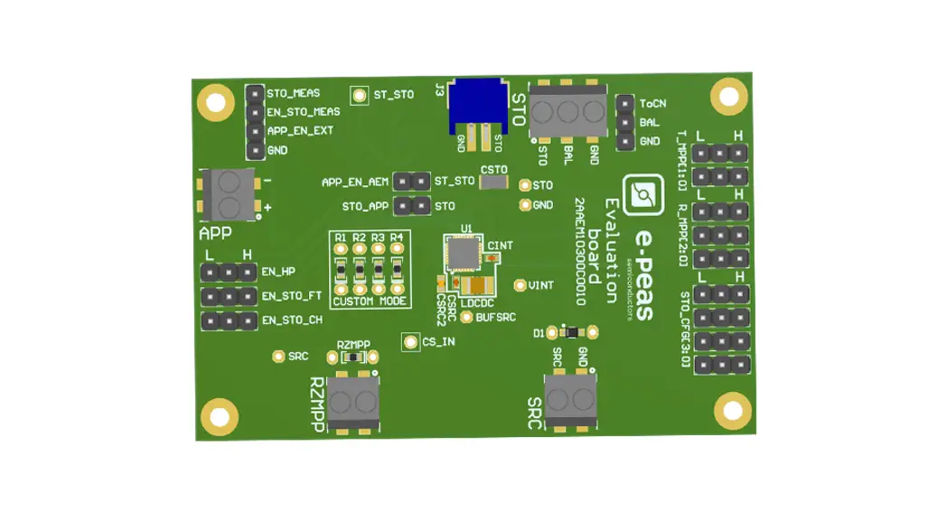
Appearance
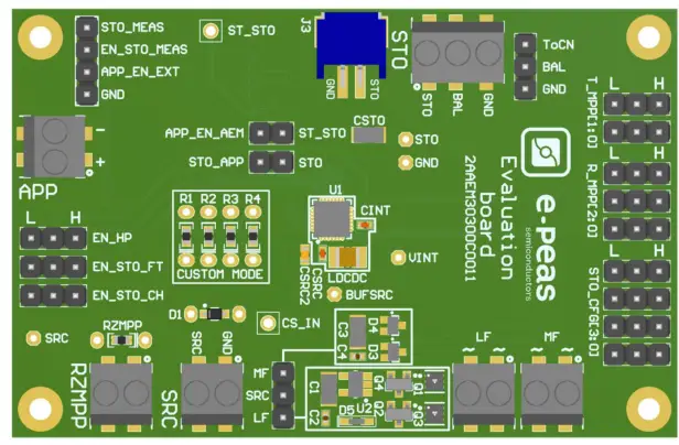
Features
Five two-way screw terminals
– Source of energy (DC)
– Source of energy (AC low frequency)
– Source of energy (AC medium frequency)
– ZMPP configuration
– External output supply
One three-way screw terminal
– Energy storage element (battery or (super)capacitor)
One 2-pin “Shrouded Header”
– Alternative connector for the storage element
Thirteen 3-pin headers
– Maximum power point ratio (R_MPP) configuration
– Maximum power point timing (T_MPP) configuration
– Energy storage element threshold configuration
– Dual-cell supercapacitor configuration
– Modes configuration
Provision for five resistors
– Custom mode configuration
– ZMPP configuration
Configuration by 0 Ohm resistors
– Cold start input configuration
One 1-pin header
– Access to status pin
Device Information
| Part Number | Dimensions |
| 2AAEM10300C0010 | 76 mm x 50 mm |
Connections Diagram
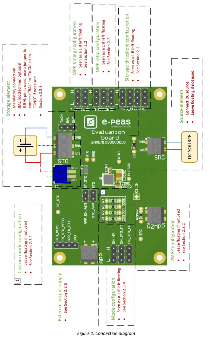
1.1. Signals Description
| NAME | FUNCTION | CONNECTION | |
| If used | If not used | ||
| Power signals | |||
| SRC | Connection to the harvested energy source. | Connect the source element. | |
| STO | Connection to the energy storage element. | Connect the storage element in addition to CSTO (150 µF). | Do not remove CSTO. |
| BAL | Connection to balancing of the dual-cell supercapacitor. | Connect balancing and place a jumper shorting BAL and “TN”. | Use a jumper to connect “BAL” to “GND”. |
| APP | Connection to the application | Connect the jumper on APP_EN_AEM and a jumper on STO_APP | Remove the jumper on APP_EN_AEM and the jumper on STO_APP |
| Debug signals | |||
| VINT | Internal voltage supply. | ||
| BUFSRC | Connection to an external capacitor buffering the buck-boost converter input. | ||
| Configuration signals | |||
| R_MPP[2:0] | Configuration of the MPP ratio. | Connect jumper | Leave floating |
| T_MPP[1:0] | Configuration of the MPP timing | Connect jumper | Leave floating |
| STO_CFG[3:0] | Configuration of the threshold voltages for the energy storage element. | Connect jumper | Leave floating |
| ZMPP | Configuration of the constant impedance MPP | Use resistor RZMPP | Leave floating |
| Control signals | |||
| EN_HP | Enabling pin for the high-power mode | Connect jumper | |
| EN_STO_FT | Enabling pin for the feed-through feature | Connect jumper | |
| EN_STO_CH | Enabling pin for the storage charging | Connect jumper | |
| APP_EN_AEM | Enabling pin for the application supply | Connect jumper | |
| APP_EN_EXT | External signal | Leave floating | |
| EN_STO_MEAS | Enabling pin for the storage element measure | External signal | Leave floating |
| Status signals | |||
| ST_STO | Logic output. Asserted when the storage device voltage rises above the VCHRDY threshold. Reset when the storage device voltage drops below the VOVDIS threshold. The high level is VSTO. | ||
| STO_MEAS | The voltage level on the storage element. | High level in EN_STO_MEAS (from the external signal) to enable the measure. | Leave floating EN_STO_MEAS |
Table 1: Pin description
General Considerations
2.1. Safety Information
Always connect the elements in the following order:
- Reset the board: Short VINT, STO, and SRC test points to GND.
- Completely configure the PCB (Jumpers/resistors);
– MPP configuration (Ratio/Timing)
– Battery Configuration
– Balancing circuit configuration
– Mode configuration - Connect the storage elements on STO.
- Connect the source (DC or AC) to the SRC connector.
To avoid damaging the board, users are required to follow this procedure. In fact, the pins BAL cannot remain floating.
2.2. Basic Configurations
| Configuration pins | Storage element threshold voltages | Typical use | |||||
| STO_CFG[3] | STO_CFG[2] | STO_CFG[1] | STO_CFG[0] | VOUCH | VCHRDY | VOVDIS | |
| 0 | 0 | 0 | 0 | 4.08 V | 3.51 V | 3.03 V | Li-ion battery |
| 0 | 0 | 0 | 1 | 3.64 V | 3.08 V | 2.82 V | LiFePO4 battery |
| 0 | 0 | 1 | 0 | 2.74 V | 2.41 V | 1.85 V | NiMH battery |
| 0 | 0 | 1 | 1 | 4.65 V | 1.00 V | 0.20 V | Dual-cell supercapacitor |
| 0 | 1 | 0 | 0 | 2.63 V | 1.00 V | 0.20V | Single-cell supercapacitor |
| 0 | 1 | 0 | 1 | 2.99 V | 1.20 V | 1.00 V | Single-cell supercapacitor |
| 0 | 1 | 1 | 0 | 2.63 V | 2.30 V | 1.85 V | NGK |
| 0 | 1 | 1 | 1 | Custom Mode | |||
| 1 | 0 | 0 | 0 | 1.49 V | 1.25 V | 1.1 V | Ni-Cd 1 cells |
| 1 | 0 | 0 | 1 | 2.99 V | 2.50 V | 2.22 V | Ni-Cd 2 cells |
| 1 | 0 | 1 | 0 | 4.65 V | 2.00 V | 1.49 V | Dual-cell supercapacitor |
| 1 | 0 | 1 | 1 | 2.63 V | 1.20 V | 1.00 V | Single-cell supercapacitor |
| 1 | 1 | 0 | 0 | 2.63 V | 2.30 V | 2.00 V | ITEN / Umal Murata |
| 1 | 1 | 0 | 1 | 4.35 V | 3.51 V | 3.03 V | Li-Po battery |
| 1 | 1 | 1 | 0 | 4.00 V | 2.70 V | 2.60 V | Tadiran TLI1020A |
| 1 | 1 | 1 | 1 | 3.92 V | 3.51 V | 2.60 V | Tadiran HLC1020 |
Table 2: Storage Element Configuration Pins
| Configuration pins | MPPT ratio | ||
| R_MPP[2] | R_MPP[1] | R_MPP[0] | VMPP / VOC |
| 0 | 0 | 0 | 60% |
| 0 | 0 | 1 | 65% |
| 0 | 1 | 0 | 70% |
| 0 | 1 | 1 | 75% |
| 1 | 0 | 0 | 80% |
| 1 | 0 | 1 | 85% |
| 1 | 1 | 0 | 90% |
| 1 | 1 | 1 | ZMPP |
Table 3: MPP Ratio Configuration Pins
| Configuration pins | MPPT timing | ||
| T_MPP[1] | T_MPP[0] | Sampling duration | Sampling period |
| 0 | 0 | 5.19 ms | 280 ms |
| 0 | 1 | 70.8 ms | 4.5 s |
| 1 | 0 | 280 ms | 17.87 s |
| 1 | 1 | 1.12 s | 71.7 s |
Table 4: MPP Timing Configuration Pins
2.3. Advanced Configurations
A complete description of the system constraints and configurations is available in Section 8 “System configuration” of the AEM10300 datasheet. A reminder on how to calculate the configuration resistors value is provided below. The calculation can be made with the help of the spreadsheet found on the e-peas website.
2.3.1. Custom Mode
In addition to the pre-defined protection levels, the custom mode allows users to define their own levels via resistors R1 to R4.
By defining RT = R1 + R2 + R3 + R4 (1 M ≤ RT ≤ 100 M)
– R1 = RT (1 V / VOVCH)
– R2 = RT (1 V / VCHRDY – 1 V / VOVCH)
– R3 = RT (1 V / VOVDIS – 1 V / VCHRDY)
– R4 = RT (1 – 1 V / VOVDIS)
Make sure the protection levels satisfy the following conditions:
– VCHRDY + 0.05 V ≤ VOVCH ≤ 4.5 V
– VOVDIS + 0.05 V ≤ VCHRDY ≤ VOVCH – 0.05 V
– 1 V ≤ VOVDIS
If unused, leave the resistor footprints (R1 to R4) empty.
2.3.2. ZMPP Configuration
If this configuration is chosen (see Table 3), the AEM10300 regulates Vsrc at a voltage equal to the product of RZMPP times the current available at the source SRC.
– 10 Ω ≤ RZMPP ≤ 1 MΩ
If unused, leave the resistor footprint RZMPP empty.
2.3.3. Balancing Circuit Configuration
When using a dual-cell supercapacitor (that does not already include a balancing circuit), enable the balun circuit configuration to ensure equal voltage on both cells. To do so:
– Connect the node between the two supercapacitor cells to BAL (on STO connector)
– Use a jumper to connect “BAL” to “ToCN”
If unused, use a jumper to connect “BAL” to “GND”
2.3.4. Mode Configuration
EN_HP
When EN_HP is pulled up to VINT, the DCDC converter is set to HIGH POWER MODE. This allows higher currents to be extracted from the buck-boost input (SRC) to the buck-boost output ( STO or VINT).
– Use a jumper to connect EN_HP to 1 to enable the high-power mode.
– Use a jumper to connect EN_HP to 0 to disable the high-power mode.
EN_STO_FT
To disable the source to storage element feed-through, the 3pin header is available.
– Use a jumper to connect the EN_STO_FT to 1 to activate the feature.
– Use a jumper to connect the EN_STO_FT to 0 to disable the feature.
2.3.5. External Output Supply
The AEM10300 is a battery charger. An external application can be supplied from the battery using the APP connector in the EVK.
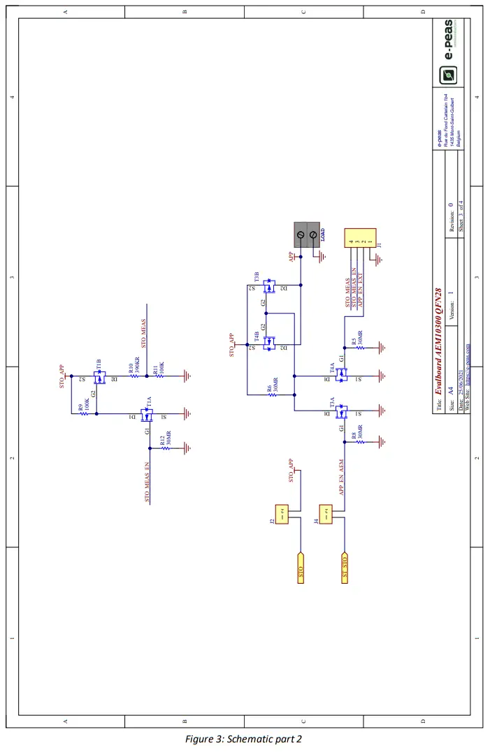
To enable this feature a jumper may be placed connecting STO to STO_APP. A switch will connect the storage element to the APP connector if one of these two signals, APP_EN_AEM or APP_EN_EXT, has a high logic level. Placing a jumper linking ST_STO and APP_EN_AEM will enable the APP output when the voltage in the storage element rises above VCHRDY (if the AEM comes from RESET STATE) and while the storage element voltages are over VOVDIS. The AEM10300 goes to RESET STATE if there is no more energy to harvest in the SRC input, the ST_STO signal is also reset. The APP_EN_EXT signal may be asserted from the application to continue using the APP output when the AEM is in RESET STATE.
The storage element voltage can be measured in the STO_MEAS pin. This pin is connected to a power-gated resistor bridge that can be enabled through the EN_STO_MEAS signal.
Functional Tests
This section presents a few simple tests that allow the user to understand the functional behavior of the AEM10300. To avoid damaging the board, follow the procedure found in Section 2.1 “Safety Information”. If a test has to be restarted make sure to properly reset the system to obtain reproducible results.
The following functional tests were made using the following setup:
– Configuration: R_MPP[2:0] = LLL, T_MPP[1:0] = LH,STO_CFG[3:0] = LLLL, EN_HP = H, EN_STO_CH = H, EN_STO_FT = L
– Storage element: Capacitor (4.7 mF + CSTO)
– SRC: current source (1mA or 100uA) with voltage compliance (4V)
The user can adapt the setup to match your system as long as you respect the input and cold-start constraints (see Section 1 “Introduction” of AEM10300 datasheet).
3.1. Start-up
The following example allows the user to observe the behavior of the AEM10300 in the Wake-up state.
Setup
– Place the probes on the nodes to be observed.
– Referring to Figure 1, follow steps 1 to 5 explained in Section 2.1 “Safety Information”.
Observations and measurements
– STO: Voltage rises as the power provided by the source is transferred to the storage element
– ST_STO: Asserted when the voltage on STO rises above VCHRDY
3.2. Shutdown
This test allows users to observe the behavior of the AEM10300 when the system is running out of energy.
Setup
– Place the probes on the nodes to be observed.
– Referring to Figure 1, follow steps 1 to 5 explained in Section 2.1 “Safety Information”. Configure the board in the desired state and start the system (see Section 3.1).
– Let the system reach a steady state (i.e. voltage on STO between VCHRDY and VOVCH and ST_STO asserted.
– Remove your source element and let the system discharge through a quiescent current.
Observations and measurements
– STO: Voltage decreases as the system consumes the power accumulated in the storage element. The voltage reaches VOVDIS.
– ST_STO: De-asserted when the storage element is running out of energy (VOVDIS).
3.3. Cold start
The following test allows the user to observe the minimum voltage required to cold-start the AEM10300. To prevent leakage current induced by the probe the user should avoid probing any unnecessary node. Make sure to properly reset the board to observe the cold-start behavior.
Setup
– Place the probes on the nodes to be observed.
– Referring to Figure 1, follow steps 1 and 2 explained in Section 2.1. Configure the board in the desired state.
Do not plug any storage element in addition to CSTO.
– SRC: Connect your source element.
Observations and measurements
– SRC: Equal to the cold-start voltage during the cold start phase. Regulated at the selected MPPT percentage of Voc when cold start is over. Be careful that the cold-start phase time will shorten with the input power. Limit it to ease the observation.
– STO: Starts to charge the storage element when the cold-start phase is over
3.4. Dual-cell supercapacitor balancing circuit
This test allows users to observe the balancing circuit behavior that maintains the voltage on BAL equilibrated. Setup
– Following steps 1 and 2 explained in Section 2.1 and referring to Figure 1, configure the board in the desired state. Plug the jumper linking “BAL” to “town”.
– STO: Plug capacitor C1 between the positive (+) and the BAL pins and a capacitor C2 between BAL and the negative (-) pins.
Select C1 ≠ C2 such that:
• C1 & C2 > 1mF
• (C2 * VCHRDY)/C1 ≥ 0.9V
– SRC: Plug your source element to start the power flow to the system
Observations and measurements
– BAL: Equal to half the voltage on STO
Do not leave BAL floating, you risk damaging the AEM.
3.5. Source to Storage Element FeedThrough
This example allows users to observe the feed-through feature.
Setup
– Place the probes on the nodes to be observed.
– Referring to Figure 1, follow steps 1 to 5 explained in Section 2.1 “Safety Information”. Configure the board in the desired state and start the system (see Section 3.1).
– Let the system reach a steady state (i.e. voltage on STO between VCHRDY and VOVCH and ST_STO asserted.
– EN_STO_FT: Connect to H
– SRC: current source (1mA or 100uA) with voltage compliance (5V)
– Put a capacitor (>1mF) on SRC and STO to avoid perturbation due to the SMU behavior.
Observations and measurements
– STO: The current from the source is transferred directly to the storage element
Schematics
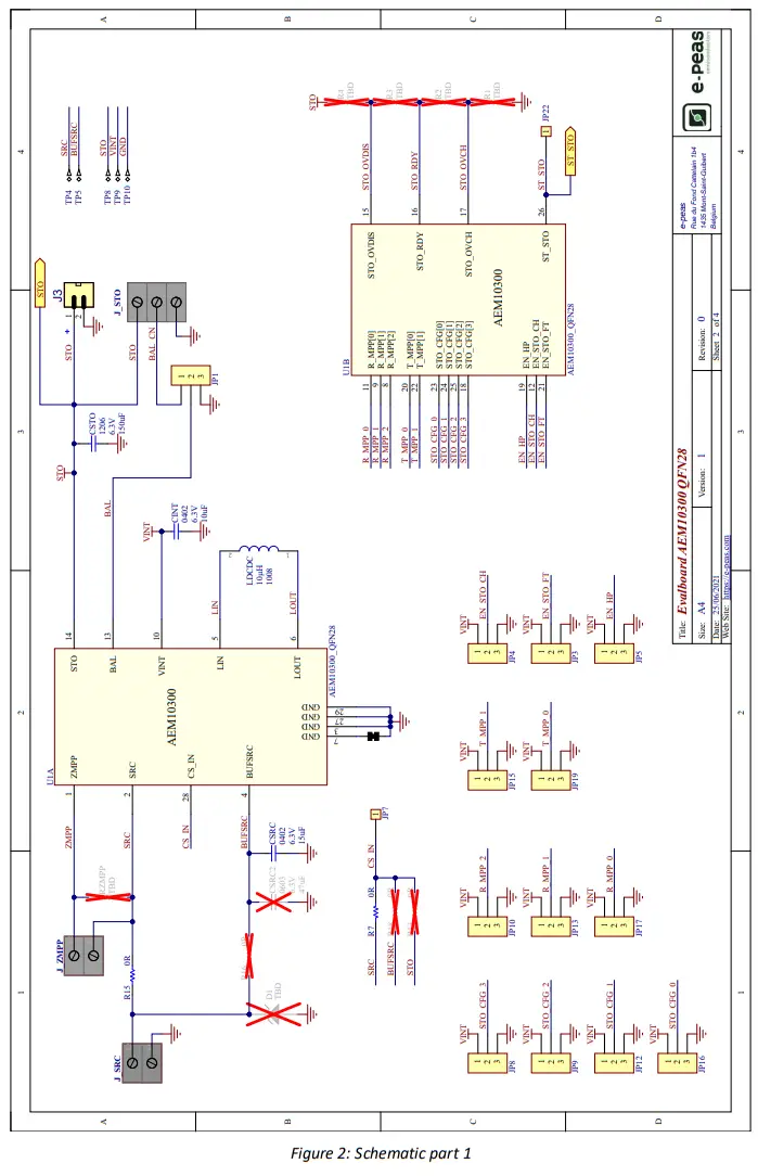
 UG_AEM10300_Rev1.0
Copyright © 2021 e-peas SA![]()


