u-blox EVK-NORA-W10 Evaluation kit
Abstract
The document describes how to set up the EVK-NORA-W101 and EVK-NORA-W106 evaluation kits to evaluate the NORA-W10 series modules. To obtain the different options for debugging and the development capabilities included in the evaluation board see the NORA-W10 system integration manual [2].
Document information
| Title | EVK-NORA-W1 | |
| Subtitle | Evaluation kit for NORA-W10 series modules | |
| Document type | User guide | |
| Document number | UBX-22002764 | |
| Revision and date | R01 | 3-May-2022 |
| Disclosure restriction | C1-Public | |
| Product status | Corresponding content status | |
| In development / Prototype | Objective specification | Target values. Revised and supplementary data will be published later. |
| Engineering sample | Advance information | Data based on early testing. Revised and supplementary data will be published later. |
| Initial production | Early production information | Data from product verification. Revised and supplementary data may be published later. |
| Mass production/ End of life | Production information | Document contains the final product specification. |
This document applies to the following products:
| Product name | Document status |
| EVK-NORA-W101 | Objective specification |
| EVK-NORA-W106 | Objective specification |
- For information about the hardware, software, and status of the available product types, see the NORA-W10 data sheet [1].
Product Description
- The EVK-NORA-W10 evaluation kit provides stand-alone use of the NORA-W10 series module.
- All features of the NORA-W10 series modules are easily accessed from the evaluation board. A simple USB connection provides power, programming, and COM ports.
- Four user buttons are available, as well as a USB peripheral connector, user LEDs, and a reset button.
- GPIO signals are available on headers that are compatible with the Arduino® form factor. This allows easy use of existing Arduino shields.
- Current sense resistors allow for measuring current into the module and into the shield.
- This guide provides setup instructions for starting development and describes the hardware functionality of the EVK-NORA-W10 board.
Key features
- Used for evaluation of NORA-W101 or NORA-W106 modules
- COM ports and debug ports over USB
- Full GPIO of the NORA-W1 series
- Buttons and LEDs for user interaction
- 32.768 kHz Crystal
- USB peripheral connector
- Power input via USB-C or pin sockets
- Current measurements via pin headers and jumpers


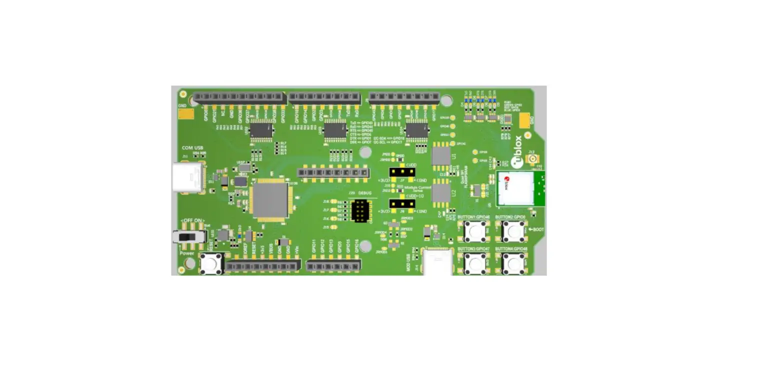
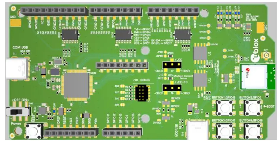
Figure 1: EVK-NORA-W10 evaluation board (top view)
Items included in the kit
EVK-NORA-W101 kit contents
- EVK-NORA-W10 evaluation board with NORA-W101 module
- USB-C to USB-A cable
- 2.4 GHz U.FL antenna kit
EVK-NORA-W106 kit contents
- EVK-NORA-W10 evaluation board with NORA-W106 module
- USB-C to USB-A cable
- 2.4 GHz antenna integrated onto NORA-W106 module (no external antenna)
Setting up the evaluation board
- The EVK-NORA-W10 is delivered without any software (open CPU) and the software must be developed by the user.
The following devices are applicable:
- EVK-NORA-W101
- EVK-NORA-W106
- The module is designed to be used only with the applicable software and only compatible software can be flashed on the module.
- Connect external power supply to the EVK as described in Powering the board. The status light (D10) (green) lights up, indicating that the internal EVK 3.3 V is on.
- When using the evaluation board with external antenna, before powering up the EVK, ensure that you have connected the 2.4 GHz antenna with the U.FL antenna connector (J12). Failing to do so may cause undesired operation.
- Observe that the inrush current when powering-up the EVK can be significantly higher than during normal operation.
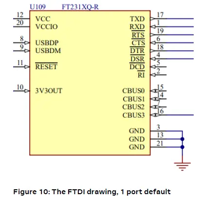
- The operating system will install the correct COM port drivers automatically. The drivers will need to be installed only when you connect the unit to a new computer for the first time. For more information about the COM ports and their configuration, see the FTDI FT231XQ-R Datasheet [3].
- One COM port will automatically be assigned to the unit by the Windows OS. To view the assigned COM ports on Windows 10, follow the steps mentioned below:
- Open the Control Panel and click Hardware and Sound.
- Click Device Manager in Devices and Printers. This will open the Device Manager window where you can view the assigned COM ports.
- The NORA-W10 open CPU variants are to be used when developing custom software based on the Espressif SDK ESP-IDF. Before compiling custom software, the ESP-IDF must be configured for the NORA-W10 open CPU variant.
- More information on this topic can be found in the NORA-W10 system integration manual [2].
Hardware description
- Design files for the EVK-NORA-W10 PCB may be requested from your local u-blox support team.
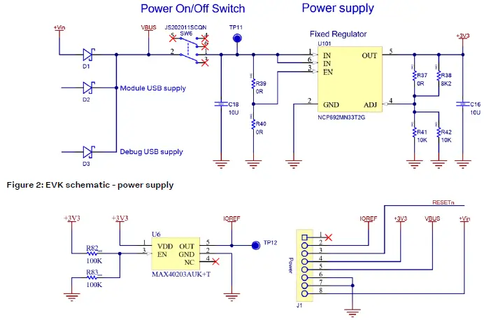
Power
The EVK-NORA-W1 has three possible power sources, as listed below:
- USB from the debug interface
- USB peripheral on the NORA-W1 itself
- 2.54 mm pitch pin header (J1 pin-8) for supplying + 5 V [ 3.6 – 5.5 V]
- Each of the three power sources is separated via a Schottky diode (D1 – D3, MBR120VLSFT3G). This prevents reverse voltage to any of the other supplies thus the power sources can be connected simultaneously.
- Only if the power protection circuits are left intact can the USB be safely connected at the same time as external power.
- This makes programming of the module easier.
- The EVK USB type C connectors are only capable of handling 5 V input, 12 V is not allowed.
Powering the board
- By moving the power switch to “ON” VBUS is fed into the 3.3 V LDO regulator and the board is powered-up.
- This is indicated by the power LED D10 (green) lights up.
- The LDO regulator powers the +3V3, VDD, and VDD-IO power rails.

- Figure 3: EVK schematic – IOREF separation
- +3V3 (J1 pin 4) can source a max of 50 mA to supply external parts.
- IOREF (J1 pin 2) is the external supply input to the IO voltage level shifters (optional). It is separated from +3V3 with a protection diode (Maxim MAX40203AUK) having a voltage drop of 28 mV at 100 mA.
Reset
- The EVK-NORA-W10 provides a hardware reset to the NORA-W10 module. The Reset button is connected to the module RESETn signal.
- If the BOOTn button is held down during the EVK power-on, it causes the module to enter its bootloader mode.

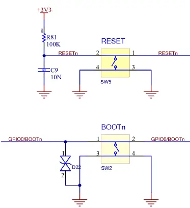
Figure 4: EVK schematic – reset and boot buttons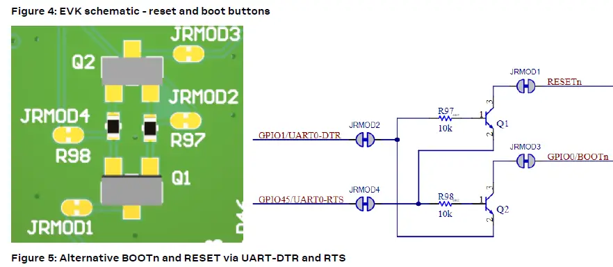
| Signal name | Description |
| GPIO0/BOOTn | GPIO0 input to module interface during normal operation. Drive low during power-up to enter bootloader mode on the NORA-W1 module. |
| RESETn | NORA-W1 reset signal. |
Table 1: EVK reset signals
- The evaluation board has four user buttons that are active low and connect to the ground when pressed. Table 2 associates the button number and corresponding components.
- The internal pull-up resistor of each NORA-W10 GPIO pin must be enabled for proper operation.
| Button | Switch | GPIO | Protection diode |
| 1 | SW1 | GPIO46 | D21 |
| 2 | SW2 | GPIO0 | D22 |
| 3 | SW3 | GPIO47 | D23 |
| 4 | SW4 | GPIO48 | D24 |
Table 2: User button components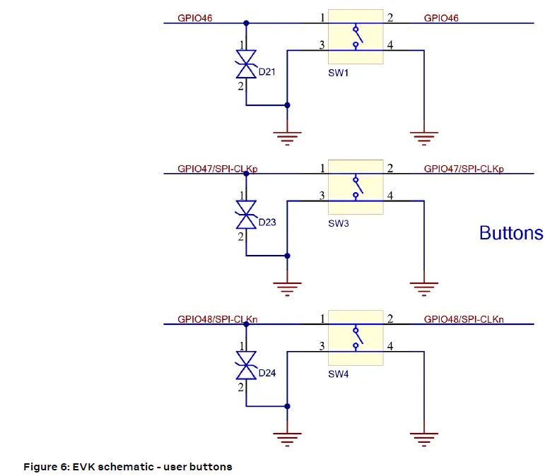
LEDs
- An RGB LED is provided on the evaluation board. It is powered by +3V3 and turned on by pulling the associated GPIO low.
- The RGB LED can be disconnected from the GPIO by removing the associated resistor R78 – R79. The evaluation board is also equipped with LEDs that show the signal status of UART0
| RGB LED | Associated GPIO | Comments |
| Red (pin1) | GPIO5/ADC1-CH4 | Remove R77 to disconnect R-LED |
| Green (pin2) | GPIO2/ADC-CH1 | Remove R78 to disconnect G-LED |
| Blue (pin3) | GPIO8/ADC1-CH7 | Remove R79 to disconnect B-LED |
Table 3: RGB LED-associated signals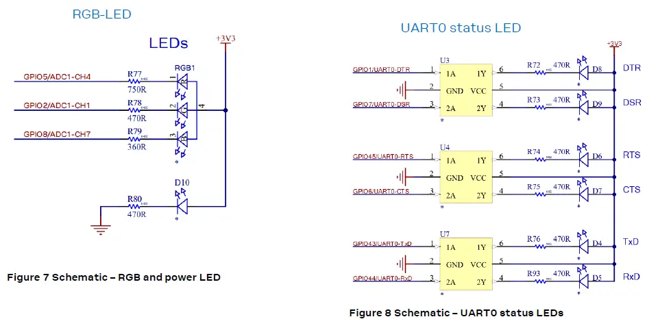
Table 4: UART0 LEDs associated signals
| LED | LED color | GPIO | Pin socket | Comments |
| D4 | Green | GPIO43/UART0-TxD | J3-7 | |
| D5 | Orange | GPIO44/UART0-RxD | J3-8 | |
| D6 | Green | GPIO45/UART0-RTS | J5-1 | |
| D7 | Orange | GPIO6/UART0-CTS | J5-2 | |
| D8 | Green | GPIO1/UART0-DTR | J5-3 | |
| D9 | Orange | GPIO7/UART0-DSR | J5-4 | |
| D10 | Green | – | Power ON LED |
Serial communication
- The evaluation board allows for easy serial communication with the NORA-W10 module and a connected computer. The EVK is using a single FTDI interface IC providing one COM port.
- The single port is connected to module UART0 through 1K resistors. This allows for simultaneously connecting UART0 signals to pin sockets J3 and J5. See also Table 5.
| NORA-W1 pin name | NORA-W1 function | Resistor/Jumper enable | Interface IC function |
| G9 | GPIO44/UART0-RxD | R20 | FTDI-TxD |
| G8 | GPIO43/UART0-TxD | R22 | FTDI-RxD |
| F9 | GPIO6/UART0-CTS | R23 | FTDI-RTS |
| F8 | GPIO45/UART0-RTS | R29 | FTDI-CTS |
| E9 | GPIO7/UART0-DSR | R30 | FTDI-DTR |
| E8 | GPIO1/UART0-DTR | R32 | FTDI-DSR |
Table 5: COM port connections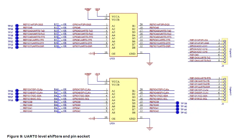
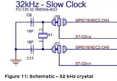
32.768 kHz low-frequency clock
- The evaluation board has a 32.768 kHz crystal connected to the NORA-W10 module to allow the use of the external crystal oscillator option
- If the signals GPIO15/ADC2-CH4 and GPIO16/ADC2-CH5 want to be used, the crystal can be removed from the circuit by opening jumpers J19 and J21 and soldering across the normally open positions. This connects XT-32k-p and XT-32k-n to the EVK pin socket J2 pin 5 and pin 6.

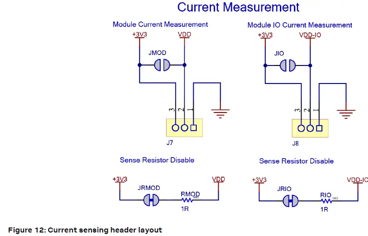
Current sensing headers
The evaluation board provides two current sensing headers:
- J7 allows for power consumption measurement of the NORA-W10 module VDD supply.
- J8 allows for power consumption measurement of the NORA-W10 module VDD-IO supply.
- Each of the 2.54 mm pitch 3-pin header have two pins connected across a 1 Ω current-sense resistor and the third pin connected to GND. Module VDD supply and module VDD-IO supply are sourced via these resistors. To measure current consumption, use a multimeter or other precision voltage measurement device to measure
- the voltage drop across pins 2 and 3. Current can also be measured directly by opening JRMOD, or JRIO to remove the current-sense resistor from the circuit. Use an amp meter in series with the two voltage pins.
- Pin 1 of J7 and J8 is connected to GND.
- Any current sense resistor can be bypassed by soldering the respective jumper: JMOD, or JIO.
- The default hardware configuration does not require any modification of the current sense headers for the EVK-NORA-W10 to perform properly.

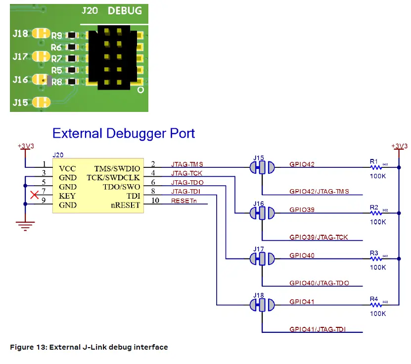
External JTAG debug interface
- External target hardware can be connected to J20 for firmware programming and debugging. The JTAG debug interface is implemented, as shown in Figure 13.
- J20 is implemented with a 2×5, header with a 1.27 mm pitch.

QSPI
- EVK-NORA-W10 can be populated with a Quad SPI FLASH and a Quad SPI PSRAM. These can be supplied via +3V3 or NORA-W10 module internal VDD-SPI supply. The selection between the two is made by populating either R11 or R69 (U1) and R70 or R71 (U2).

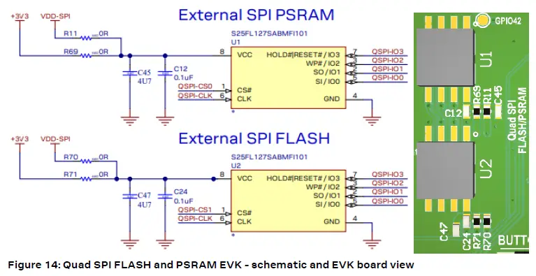
Table 6: Quad SPI interface signal overview
| Interface function | ESP32-S3 pin | NORA-W10 pin | Interface IC function |
| QSPI-CS0 | 28 | E1 | |
| QSPI-CS1 | 32 | C4 | |
| QSPI-CLK | 33 | F1 | |
| QSPI-IO3 HD | 30 | F2 | |
| QSPI-IO2 WP | 31 | D1 | |
| QSPI-IO1 Q | 34 | E2 | |
| QSPI-IO0 D | 35 | D2 |
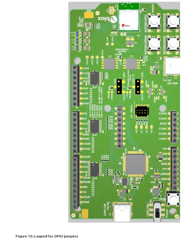
GPIO jumpers
- Several solder bridge jumpers on the board are available to configure the GPIO functions.
- Most solder jumpers disconnect onboard components from the GPIO nets thus eliminating interference with external circuitry added on the I/O sockets (female).
- The GPIO jumpers and associated functions are shown on the bottom of the EVK-NORA-W10 PCB.

Header pin-out
- Figure 14 shows the 2.54 mm pitch sockets exposing the IO signals in the NORA-W10 module.

- To enable the EVK-NORA-W10 I/O pins to handle 5 V signals the level shifters (U102 – U104, TI TXS0108EPWR) must be populated and IOREF must be supplied with +5 V. If using 3.3 V on the EVK-NORA-W1 I/O pins, the Arduino Uno® style shields must be configured to use +3.3 V I/O voltage reference.
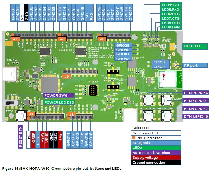
Table 7: Header J1Table 7 – Table 12 show the pin assignments of each header.
| Pin | Pin name | NORA-W1 pin | Function |
| 1 | NC. | – | No connection |
| 2 | IOREF | – | Level shifter supply voltage |
| 3 | RESET | J3 | ESP-GPIO/AIN6 |
| 4 | +3V3 | – | Supply |
| 5 | VBUS | Supply | |
| 6 | GND | Ground | |
| 7 | GND | Ground | |
| 8 | +Vin | Supply |
Table 7: Header J1
| Pin | Pin name | NORA-W1 pin PT1/PT2 | Function |
| 1 | GPIO11 | G3 | GPIO ADC2-CH0 |
| 2 | GPIO12 | G2 | GPIO ADC2-CH1 |
| 3 | GPIO13 | A6 | GPIO ADC2-CH2 |
| 4 | GPIO5 | J8 | GPIO ADC1-CH4 |
| 5 | GPIO15 | C6 | GPIO ADC2-CH4, XTAL-32K-P |
| 6 | GPIO16 | B6 | GPIO ADC2-CH5, XTAL-32K-N |
Table 8: Header J2
| Pin | Pin name | NORA-W1 pin | Function |
| 1 | GPIO10 | H3 | FSPI-IO4 |
| 2 | GPIO14 | A5 | FSPI-DQS |
| 3 | GPIO2 | H8 | ADC1-CH1 |
| 4 | GPIO3 | J9 | ADC-CH2 |
| 5 | GPIO4 | D8 | ADC1-CH3 |
| 6 | GPIO46 | H7 | GPIO46 |
| 7 | TxD | G8 | GPIO43 |
| 8 | RxD | G9 | GPIO44 |
Table 9: Header J3
| Pin | Pin name | NORA-W1 pin | Function |
| 1 | GPIO0 | F7 | BOOTn |
| 2 | GPIO21 | C8 | GPIO21 |
| 3 | NC. | – | |
| 4 | GND | – | |
| 5 | GPIO36 | B1 | FSPI-CLK |
| 6 | GPIO37 | C1 | FSPI-Q |
| 7 | GPIO35 | C2 | FSPI-D |
| 8 | GPIO34 | B3 | FSPI-CS0 |
| 9 | GPIO38 | A2 | FSPI-WP |
| 10 | GPIO33 | D3 | FSPIHD |
Table 10: Header J4
| Pin | Pin name | NORA-W1 pin | Function |
| 1 | GPIO45 | F8 | RTS |
| 2 | GPIO6 | F9 | CTS |
| 3 | GPIO1 | E8 | DTR |
| 4 | GPIO7 | E9 | DSR |
| 5 | GPIO47 | F3 | SPICLK_P |
| 6 | GPIO48 | E3 | SPICLK_N |
| 7 | GPIO18 | B4 | SDA |
| 8 | GPIO17 | A3 | SCL |
Table 11: Header J5
| Pin | Pin name | NORA-W1 pin | Function |
| 1 | +3V3 | – | Supply |
| 2 | JTAG-TMS | H2 | GPIO42 if J15 is changed |
| 3 | GND | – | Ground |
| 4 | JTAG-TCK | J2 | GPIO-39 if J16 is changed |
| 5 | GND | – | Ground |
| 6 | JTAG-TDO | G1 | GPIO40 if J17 is changed |
| 7 | NC. | – | No connection |
| 8 | JTAG-TDI | H1 | GPIO41 if J18 is changed |
| 9 | GND | – | Ground |
| 10 | RESET | J3 | Module reset |
Table 12: Header J20
Appendix A Glossary
| Abbreviation | Definition |
| ARM | Arm (Advanced RISC Machines) Holdings |
| CPU | Central Processing Unit |
| CTS | Clear To Send |
| DC | Direct Current |
| DC-DC | DC to DC converter |
| DFU | Device Firmware Update |
| EVK | Evaluation Kit |
| FICR | Factory Information Configuration Register |
| GPIO | General Purpose Input / Output |
| LDO | Low Drop-Out voltage regulator |
| LE | Low Energy |
| LED | Light Emitting Diode |
| LF | Low Frequency |
| LiPo | Lithium-Polymer battery |
| NCS | nRF Connect SDK |
| NFC | Near-Field Communications |
| QSPI | Quad Serial Peripheral Interface |
| RC | Resistor-Capacitor network |
| RTS | Request To Send |
| RXD | Receive data signal |
| SES | SEGGER Embedded Studio |
| SIG | Special Interest Group |
| SoC | System on Chip |
| SPI | Serial Peripheral Interface |
| TXD | Transmit data signal |
| PRICE | User Information Configuration Register |
| USB | Universal Serial Bus |
Table 13: Explanation of the abbreviations and terms used
- NORA-W10 data sheet, UBX-21036702
- NORA-W10 system integration manual, UBX-22005601
- FTDI FT231XQ-R Datasheet, FT231X (ftdichip.com)
- For product change notifications and regular updates of u-blox documentation, register on our website, www.u-blox.com.
Revision history
| Revision | Date | Name | Comments |
| R01 | 29-04-2022 | ovik, hekf | Initial release for EVK-NORA-W1 PT2 |
Contact
- For complete contact information, visit us at www.u-blox.com.
- u-blox Offices
- North, Central, and South America
u-blox America, Inc.
- Phone: +1 703 483 3180
- E-mail: [email protected]
- Regional Office West Coast: Phone: +1 408 573 3640
- E-mail: [email protected]
Technical Support:
- Phone: +1 703 483 3185
- E-mail: [email protected]
Headquarters
- Europe, the Middle East, Africa
- u-blox AG
- Phone: +41 44 722 74 44 E-mail: [email protected] Support: [email protected]
Asia, Australia, Pacific
- u-blox Singapore Pte. Ltd.
- Phone: +65 6734 3811
- E-mail: [email protected] Support: [email protected]
Regional Office Australia:
- Phone: +61 3 9566 7255
- E-mail: [email protected] Support: [email protected]
Regional Office China (Beijing):
- Phone: +86 10 68 133 545
- E-mail: [email protected] Support: [email protected]
Regional Office China (Chongqing):
- Phone: +86 23 6815 1588
- E-mail: [email protected] Support: [email protected]
Regional Office China (Shanghai):
- Phone: +86 21 6090 4832
- E-mail: [email protected] Support: [email protected]
Regional Office China (Shenzhen):
- Phone: +86 755 8627 1083
- E-mail: [email protected] Support: [email protected]
Regional Office India:
- Phone: +91 80 405 092 00
- E-mail: [email protected] Support: [email protected]
Regional Office Japan (Osaka):
- Phone: +81 6 6941 3660
- E-mail: [email protected] Support: [email protected]
Regional Office Japan (Tokyo):
- Phone: +81 3 5775 3850
- E-mail: [email protected] Support: [email protected]
Regional Office Korea:
- Phone: +82 2 542 0861
- E-mail: [email protected] Support: [email protected]
Regional Office Taiwan:
- Phone: +886 2 2657 1090
- E-mail: [email protected] Support: [email protected]


