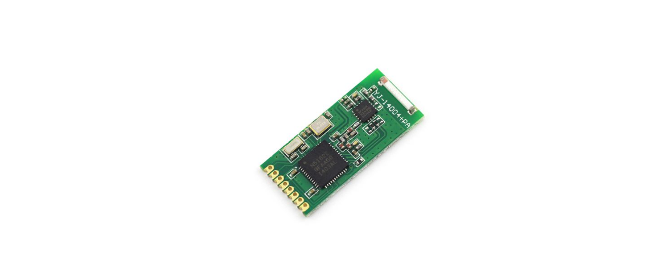
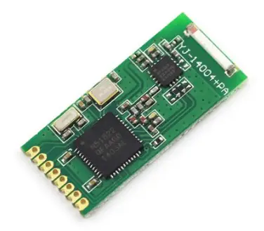
Waterpik 20028186 Bluetooth Low Energy Radio Module
WATERPIK BLUETOOTH LOW ENERGY MODULE USER MANUAL
The 20028186 module has been evaluated in stand-alone conditions. For different operational conditions from a stand-alone modular transmitter in a host (multiple, simultaneously transmitting modules, or other transmitters in a host), may require additional testing. If this module is intended for use in a portable device, you are responsible for separate approval to satisfy the SAR requirements of FCC Part 2.1093. The modular transmitter is only FCC authorized for the specific rule parts (i.e., FCC transmitter rules) listed on the grant, and the host product manufacturer is responsible for compliance to any other FCC rules that apply to the host not covered by the modular transmitter grant of certification. If the grantee markets their product as being Part 15 Subpart B compliant (when it also contains unintentional-radiator digital circuitry), then the grantee shall provide a notice stating that the final host product sill requires Part 15 Subpart B compliance testing with the modular transmitter installed. The end product with an embedded module may also need to pass the FCC Part 15 unintentional emission testing requirement and be properly authorized per FCC Part 15.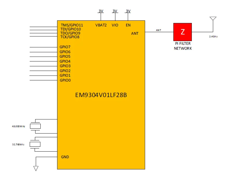
This module is not intended to transmit simultaneously with any other antenna or transmitter. The host end product must include a user manual that clearly defines operating requirements and conditions that must be observed to ensure compliance with current FCC RF exposure guidelines. The final host/module combination may also need to be evaluated against the FCC Part 15B criteria for unintentional radiators in order to be properly authorized for operation as a Part 15 digital device. The User’s Manual or Instruction Manual for an intentional or unintentional radiator shall caution the user that changes for modifications not expressly approved by the party responsible for compliance could void the user’s authority to operate the equipment. In cases where the manual is provided only in a form other than paper, such as on a computer disk or over the Internet, the information required by this section may be included in the manual in that alternative form, provided the user can reasonably be expected to have the capability to access information in that form.
To ensure compliance with all non-transmitter functions the host manufacturer is responsible for ensuring compliance with the modules(s) installed and operational. For example, if a host was previously authorized as an unintentional radiator under the declaration of Conformity procedure without a transmitter certified module and a module is added, the host manufacturer is responsible for ensuring that the after the module is installed and operational the host continues to be compliant with the Part 15B unintentional radiator requirements.
VERSION HISTORY
| Version | Comment |
| 0.0 | Initial Draft |
| 0.1 | Updated regulatory certifications |
| 1.0 | Removed Schematics and Bill of Material and updated Figure reference. Initial Release |
| 1.1 | Added ISED sections |
| 1.2 | Adjustments to exposure limits |
| 1.3 | Correct numbering |
DESCRIPTION
Features:
- System-on-a-Chip Core:
- ARC EM4 32-bit MCU running at 24MHz
- Floating-point unit for supporting sensor processing
- 128KB OTP (for parameters, profiles, and applications)
- 48KB instructions RAM
- 28KB Data RAM
- I2C and SPI master interfaces
- Up to 12 GPIOs
- Optimized Bluetooth 5.0 Low Energy 2.4GHz RF Transceiver
- Bluetooth stack in ROM
- SPI and UART HCI/ACI Transport Layers
- Up to 8 simultaneous connections supported
- Extended PDU length and enhanced security
- Firmware Over-the-Air (FOTA) updating
- Secure
- True Random Number Generator
- AES-128 Hardware Encryption Engine
- Key Generation (ECC-P256)
- Onboard step-down DC to DC converter
- High-performance RF:
- -34dBm to +6.1dBm output transmit power range
- ISM Band 2.405GHz – 2.48GHz Operation
- Small size: 0.450” x 0.645” x 0.077”, surface Mountable
- Integrated crystals (48MHz and 32.768KHz), Internal Voltage Regulator, Matching Circuitry and PCB Antenna
- Radio Regulation Certifications for the United States (FCC), Canada (IC), and Europe (ETSI)
- Up to 400 ft. Range
Operational
- Operating Voltage: 1.9V – 3.6V (Module Configured for Buck Operation)
- Temperature Range: -40°C – 85°C
- Low-Current Consumption:
- RX Mode: 3.0mA (typical)
- TX Mode: 5.2mA (typical) peak transmitter current at 0.4dBm
- Sleep: 1.0µA connected
- Bluetooth low energy Receiver Sensitivity: -94dBm (1Mbps operation and 37-byte payload)
PINOUT AND TERMINAL DESCRIPTION
The pin diagram for the 20028186 module is as follows: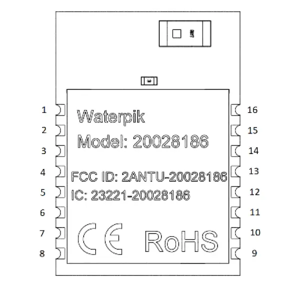
The available pins are:
| MODULE PIN | PIN NAME | DESCRIPTION | PRIMARY FUNCTION | ALTERNATIVE FUNCTION |
| 1 | GND | Ground pin for the module | GROUND |
See Figure 3 |
| 2 | VBAT2 | Power input (VCC), 1.9V to 3.6V | VCC | |
| 3 | VIO | Voltage reference pin for IO. Connect to VBAT2 | VCC2 | |
| 4 | EN | Chip enable. Active high. | ENABLE | |
| 5 | GPIO5 | General Purpose Input/Output pin | GPIO | |
| 6 | GPIO6 | General Purpose Input/Output pin | GPIO | |
| 7 | GPIO0 | General Purpose Input/Output pin | GPIO | |
| 8 | GPIO1 | General Purpose Input/Output pin | GPIO | |
| 9 | GPIO2 | General Purpose Input/Output pin | GPIO | |
| 10 | GPIO3 | General Purpose Input/Output pin | GPIO | |
| 11 | GPIO7 | General Purpose Input/Output pin | GPIO | |
| 12 | GPIO4 | General Purpose Input/Output pin | GPIO | |
| 13 | GPIO8 | General Purpose Input/Output pin | GPIO | TCK (JTAG) |
| 14 | GPIO9 | General Purpose Input/Output pin | GPIO | TDO (JTAG) |
| 15 | GPIO10 | General Purpose Input/Output pin | GPIO | TDI (JTAG) |
| 16 | GPIO11 | General Purpose Input/Output pin | GPIO | TMS (JTAG) |
The GPIO pins can be further mapped for the following functions: 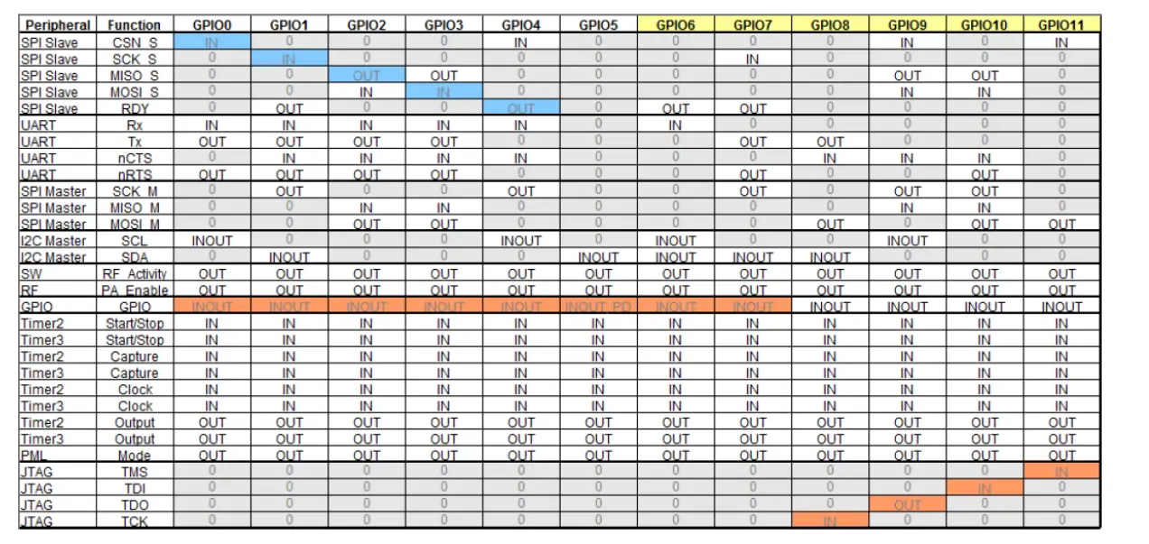
GPIO Pins can be configured as digital input, push-pull output, or selectable pull-down/pull-up resistors. There are 3.3V standard protections against VSS and VIO. Peripherals for the module include I2C master, SPI master and slave, UART, GPIO, and timers. Flow control is included for SPI slave mode maximum transfer efficiency. Both the I2C master and SPI master have 16-byte buffers. Both UART slave and SPI slave have FIFOs implemented for 64-byte FIFOs for RX and TX and 1 to 4 byte register reads from RX FIFO or writes to TX FIFO. FIFO status registers and interrupts are available for many different conditions.
ELECTRICAL CHARACTERISTICS
The information provided (below) is based on information provided from the EM Microelectronic EM9304 Datasheet and has not been independently verified for accuracy.
| PARAMETERS | CONDITION | MINIMUM | TYPICAL | MAXIMUM | UNITS |
| Supply Voltage for VBAT2, VIO | DC to DC step-down | 1.91 | 3.3 | 3.6 | V |
| Schmidt Trigger Hysteresis | 0.05 X VIO | V | |||
| Input High Voltage (VIH) | VIO ≥ 1.9V | 0.7 X VIO | – | – | V |
| VIO < 1.9V | 0.85 X VIO | – | – | ||
| Input Low Voltage (VIL) | VIO ≥ 1.9V | – | 0.3 X VIO | V | |
| VIO < 1.9V | 0.15 X VIO | V | |||
| Output High Voltage High | IOUT = -3mA, VIO = 1.9V | 1.5 | – | – | V |
| IOUT = -8mA, VIO = 1.9V | 0.84 | – | – | V | |
| Output Low Voltage Low | IOUT = 3mA, VIO = 1.9V | – | – | 0.4 | V |
| IOUT = 0.8mA, VIO = 1.9V | – | – | 0.21 | V | |
| Pull Up resistor GPIO5 | 8 | 10 | 18 | KΩ | |
| Pull Up resistor GPIO | 70 | 100 | 130 | KΩ | |
| Ambient Operating Temperature | -40 | – | +85 | °C |
2.3V is required for OTP programming.
| PARAMETERS | MINIMUM | TYPICAL | MAXIMUM | UNITS |
| RX Mode | – | 3.0 | – | mA |
| TX Mode, TX Power Level 0 | – | 2.2 | – | mA |
| TX Mode, TX Power Level 1 | – | 2.4 | – | mA |
| TX Mode, TX Power Level 2 | – | 2.8 | – | mA |
| TX Mode, TX Power Level 3 | – | 2.9 | – | mA |
| TX Mode, TX Power Level 4 | – | 3.0 | – | mA |
| TX Mode, TX Power Level 5 | – | 3.1 | – | mA |
| TX Mode, TX Power Level 6 | – | 3.2 | – | mA |
| TX Mode, TX Power Level 7 | – | 3.3 | – | mA |
| TX Mode, TX Power Level 8 | – | 3.4 | – | mA |
| TX Mode, TX Power Level 9 | – | 3.6 | – | mA |
| TX Mode, TX Power Level 10 | – | 3.8 | – | mA |
| TX Mode, TX Power Level 11 | – | 4.1 | – | mA |
| TX Mode, TX Power Level 12 | – | 4.3 | – | mA |
| TX Mode, TX Power Level 13 | – | 4.6 | – | mA |
| TX Mode, TX Power Level 14 | – | 5.2 | – | mA |
| TX Mode, TX Power Level 15 | – | 5.6 | – | mA |
| TX Mode, TX Power Level 16 | – | 7.5 | – | mA |
| TX Mode, TX Power Level 17 | – | 9.9 | – | mA |
| Active RC1 | – | 0/2 | – | mA |
| Active XTAL1 | – | 0.4 | – | mA |
| ECC ROM Execution in a loop | – | 0.7 | – | mA |
| Coremark test from IRAM1 | – | 1.2 | – | mA |
| Coremark test from OTP | – | 1.6 | – | mA |
| Sleep Mode, LF RC | – | 1.0 | – | mA |
| Sleep Mode, LF XTAL | – | 0.95 | – | mA |
| Deep Sleep Mode | – | 0.65 | – | mA |
| Chip Disabled | – | 5 | – | mA |
| Battery Peak Currents2 | – | 10.3 | – | mA |
CPU halted.
Typical value using pi-filter. Valid for 0dBm TX power level and below
| PARAMETERS | CONDITION | MINIMUM | TYPICAL | MAXIMUM | UNITS |
| Step-Down, DCDC off | VBAT = 3.0V, Ramp = 0.3V/µs, LF RC | – | 3.6 | – | ms |
| Any | 32KHz crystal or external signal used | – | 1.2 | – | s |
| MODE 1 | MODE 2 | CONDITION | MINIMUM | TYPICAL | MAXIMUM | UNITS |
| Sleep | Active XTAL | HCI/ACI Command RDY (Depends on Crystal Q) | – | 1.1 | – | ms |
| PARAMETERS | CONDITION | MINIMUM | TYPICAL | MAXIMUM | UNITS |
| Output Low Voltage | IOUT = 3mA, VIO = 1.9V | 0.1 | – | – | V |
| IOUT = 2mA, VIO = 1.9V | 0.21 | – | – | V |
| PARAMETERS | CONDITION | MINIMUM | TYPICAL | MAXIMUM | UNITS |
| Output Delay, Falling Edge (VBAT = 1.05V to 3.6V) | Output Load = 25pF | – | – | 500 | ns |
| Output Load = 150pF | – | – | 520 | ns | |
| Output Load = 400pF | – | – | 540 | ns |
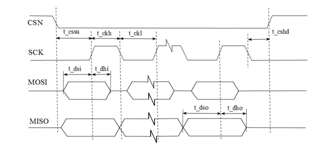
| PARAMETERS | Symbol | MINIMUM | TYPICAL | MAXIMUM | UNITS |
| Clock Frequency Slave | t_frq_s | 16 | MHz | ||
| Clock Frequency Master | t_frq_m | 6 | MHz | ||
| Data Setup Time (input) | t_dsi | 10 | ns | ||
| Data Hold Time (input) | t_dhi | 10 | ns | ||
| Data Setup Time (output) | t_dso | (1/t_frq)-46ns | ns | ||
| Data Hold Time | t_dhd | 13 | ns | ||
| CSN Setup Time | t_cssu | 100 | ns | ||
| CSN Hold Time | t_cshd | 100 | ns | ||
| Data Setup Time Master (input) | t_dsim | 35 | ns | ||
| Data Hold Time Master (input) | T_dhim | 10 | ns |
| PARAMETERS | Symbol | MINIMUM | TYPICAL | MAXIMUM | UNITS |
| Clock Frequency Slave | t_frq_s | 8 | MHz | ||
| Clock Frequency Master | t_frq_m | 3 | MHz |
| Clock Pulse Width Low | t_clkl | 0.4/t_frq | µs | ||
| Clock Pulse Width High | t_clkh | 0.4/t_frq | µs | ||
| Data Setup Time (input) | t_dsi | 10 | µs | ||
| Data Hold Time (input) | t_dhi | 10 | µs | ||
| Data Setup Time (output) | t_dso | (1/t_frq)-46ns | µs | ||
| Data Hold Time | t_dhd | 13 | µs | ||
| CSN Setup Time | t_cssu | 100 | µs | ||
| CSN Hold Time | t_cshd | 100 | µs | ||
| Data Setup Time Master (input) | t_dsim | 60 | µs | ||
| Data Hold Time Master (input) | T_dhim | 10 | µs |
| PARAMETERS | CONDITION | MINIMUM | TYPICAL | MAXIMUM | UNITS |
| RF Input Frequency | Compatible to IEEE 802.15.4, 2003 | 2.405 | – | 2.480 | GHz |
| RF Sensitivity | 1Mbps, 37 byte payload | – | -94 | – | dBm |
| 1Mbps, 255 byte payload | – | -93 | – | dBm | |
| Maximum Input Power | 1Mbps, 255 byte payload | – | 0 | – | dBm |
| PARAMETER | COMMENT | SYMBOL | MINIMUM | TYPICAL | MAXIMUM | UNITS |
|
Output Power | TX Power Level 0 | PTX0 | – | -33.5 | – | dBm |
| TX Power Level 1 | PTX1 | – | -29.0 | – | dBm | |
| TX Power Level 2 | PTX2 | – | -17.9 | – | dBm | |
| TX Power Level 3 | PTX3 | – | -16.4 | – | dBm | |
| TX Power Level 4 | PTX4 | – | -14.6 | – | dBm | |
| TX Power Level 5 | PTX5 | – | -13.1 | – | dBm | |
| TX Power Level 6 | PTX6 | – | -11.4 | – | dBm | |
| TX Power Level 7 | PTX7 | – | -9.9 | – | dBm | |
| TX Power Level 8 | PTX8 | – | -8.4 | – | dBm | |
| TX Power Level 9 | PTX9 | – | -6.9 | – | dBm | |
| TX Power Level 10 | PTX10 | – | -5.5 | – | dBm | |
| TX Power Level 11 | PTX11 | – | -4.0 | – | dBm | |
| TX Power Level 12 | PTX12 | – | -2.6 | – | dBm | |
| TX Power Level 13 | PTX13 | – | -1.4 | – | dBm | |
| TX Power Level 14 | PTX14 | – | 0.4 | – | dBm | |
| TX Power Level 15 | PTX15 | – | 2.5 | – | dBm | |
| TX Power Level 16 | PTX16 | – | 4.6 | – | dBm | |
| TX Power Level 17 | PTX17 | – | 6.2 | – | dBm | |
| Power in 2nd harmonic | Output power step = 17 50Ω for typical value. PT for maximum value. | PTX2 | – | -50 | – | dBm |
| Power in 3rd harmonic | PTX3 | – | -60 | – | dBm | |
| Power in 4th harmonic | PTX4 | – | -60 | – | dBm | |
| Deviation from the channel center frequency | Δfc | -150 | – | 150 | KHz | |
| Frequency drift for any packet length | Δfcpkt | – | – | 50 | KHz | |
| Drift rate | Δfc/ΔT | – | – | 400 | Hz/µs | |
| Modulated Frequency Deviation | Δfmod | – | ±250 | – | KHz | |
| In-band spurious emissions, power transmitted outside the selected channel, at a frequency offset foffs | |foffs| = 2MHz |
POUT (fc+foffs) | – | – | -20 | dBm |
| |foffs| ≥ 3MHz | – | – | -30 | dBm |
REGULATORY CERTIFICATIONS
Changes or modifications not expressly approved by the manufacturer could void the user’s authority to operate the equipment. This device complies with Part 15 of the FCC Rules. Operation is subject to the following two conditions: This device may not cause harmful interference, and this device must accept and interference received, including interference that may cause undesired operation. The 20028186 Module is modular certified and complies with the following regulatory requirements:
US FCC:
EMC
- FCC CFR 47, Part 15, Subpart B (10-1-17 Edition), Secs. 15.109
- FCC Part 15.247, 10-1-17 Edition: Operation within the bands 902 – 928MHz, 2400 – 2483.5MHz, and 5725 – 5850MHz.
- FCC Part 15.209, 10-1-17 Edition: Radiated emission limits; general requirements.
CANADA – IC
- ICES-003 Issue 6 – Update April (2017).
- RSS-247 Issue 2 (February 2017).
- RSS-Gen Issue 4 (November 2014).
CE
The module conforms with RED Radio Equipment Directive 2014/53/EU, following the provisions of ERP Directive 2009/125/EC, EU RoHS Directive 2011/65/EU, including the amendment 2015/863/EU.
EMC
- ETSI EN 301 489-1 V2.2.0
- ETSI EN 301 489-17 V3.2.0
- ETSI EN 300 328 v2.2.2 (2019-07)
ISED REFULATORY NOTICES
Changes or modifications not expressly approved by the party responsible for compliance could void the user’s authority to operate the equipment. This device complies with ISED license-exempt RSS(S). Operation is subject to the following two conditions:
- This device may not cause harmful interference.
- This device must accept any interference received, including interference that may cause undesired operation.
ISED LABELLING REQUIREMENTS FOR HOST DEVICE
The host deice shall be properly labelled to identify the modules within the host device. The certification label of the module shall be clearly visible at all times when installed in the host device, otherwise, the host device must be labeled to display the IC of the module, preceded by the words “Contain transmitter module”, or the word “Contains”, or similar wording expressing the same meaning as follows: Contains IC: 23221-20028186
RF EXPOSURE SAFETY ISED
This device complies with the ISED RF exposure limits and has been evaluated in compliance with portable exposure condition. To comply with the measured SAR value/SAR testing exclusion, the equipment must be installed and operated with a minimum distance of 5 mm of the human body.
PERMITTED ANTENNA
Radio transmitter model, FCC ID: 2ANTU-20028186, has been approved by the FCC to operate with the antenna listed below with the maximum permissible gain indicated (below). Antenna types not listed below, or having a gain greater than the maximum gain indicated below, are strictly prohibited for use with this device.
| Approved Antenna | Antenna Type | Maximum Gain |
| Abracon AMCA31-2R450G-S1F-T | Surface mount Chip | 0.5dBi |
LABELING REQUIREMENTS
The module itself will have the following information displayed on its RF shield: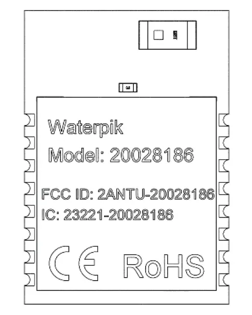
The label has the following contents:
- Model: 20028186
- FCC ID: 2ANTU-20028186
- IC ID: 23221-20028186
- FCC, CE, and RoHS markings
- Waterpik company name
In addition to the module labelling, the Host device shall properly label the end device to identify the modules within the host device. The certification label of the module shall be visible at all times when installed in the host device, or the host device must be labelled to display the IC of the module. The IC of the module must be preceded by the words “Contains transmitter module”, “Contains”, or similar wording to express similar meaning as: Contains FCC ID: 2ANTU-20028186
ENVIRONMENTAL SAFETY
The 20028186 is compliant with:
- RoHS, according to EU Directive 2011/65/EU and its amendments including 2015/863/EU
- Halogen-Free according to IEC 61249-2-21:2003
- REACH compliant according to EU Regulation 1907/2006
RF EXPOSURE SAFETY
This device complies with the FCC RF exposure limits and has been evaluated in compliance with portable exposure conditions. To comply with the measured SAR value/SAR testing exclusion, the equipment must be installed and operated with a minimum distance of 5 mm of the human body.
REFERENCE DOCUMENTS
EM9304 Device Specifications (Datasheet) Abracon LLC AMCA31-2R450G-S1F-T Datasheet


