VitalTech VT-RT6MB Bluetooth Low Energy Module
INTRODUCTION
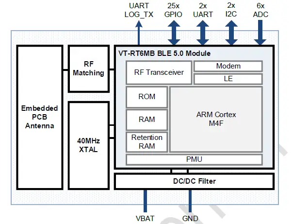
VT-RT6MB is an ultra-low-power SoC module for Bluetooth® 5.0 low energy applications that combines the excellent performance of a leading RF transceiver with a low-power ARM® Cortex-M4F and rich powerful supporting features and peripherals. The VT-RT6MB supports BLE related applications Bluetooth® and mesh networking specification suited for large-scale device networks to support building automation, sensor networks, asset tracking and other solutions where multiple devices need to communicate reliably and securely.
FEATURES
- Bluetooth® Core Spec v5.0 compliant
- Supports 2Mbps LE, LE advertising extension and LE long range
- Supports Bluetooth Mesh Network Specification
- Supports AES128/192/256 encryption/decryption
- Supports OTA (Over-the-Air) for firmware upgrade
- Battery Supply Voltage 1.8V to 3.6V
- Operational Temperature -30°C to +85°C
- Current Consumptions
- Power Down Mode 450nA (Typ.)
- Deep LPS (with 160K SRAM retention) Mode 2.5uA (Typ.)
- TX Mode (+0dBm) 8.4mA (Typ.)
- TX Mode (+4dBm) 10.4mA (Typ.)
- TX Mode (+8dBm) 12.7mA (Typ.)
- RX Mode 6.8mA (Typ.)
- Radio Bluetooth® Qualification (End Product, QDID: TBD)
- Meets Radio Certification FCC, RED, KCC and MIC Japan
- Dimension 12mm(W) x 18.82mm(L) x 2.3mm(H)
- Pb Free, RoHS Compliant
REVERSION HISTORY
| Version Code | Date | Descriptions |
| 0.1 BETA | 9-MAY-22 | Preliminary release |
| 0.2BETA | 8-AUG-22 | Modify module Description |
Notice:
The information described in this document is the exclusive intellectual property of Vital Tech. Limited and shall not be reproduced without permission from Vital Tech.
Vital Tech assumes no responsibility for errors or omissions. All data and specifications are subject to change without notice.
MODULE SPECIFICATIONS
| Specification Name | Descriptions | |
| Module Dimension | 12mm(W) x 18.82mm(L) x 2.3mm(H) | |
| BLE Core Compliant | BLE V5.0 | |
| Operation Distance | Up to 80Meters (*LE 1M, module to module testing results) | |
| Power Supply | 1.8V – 3.6V | |
|
Power Consumption | Power Down Mode | 450nA |
| Deep LPS | 2.5uA | |
| TX mode (+0dBm) | 8.4mA | |
| TX mode (+4dBm) | 10.4mA | |
| TX mode (+8dBm) | 12.7mA | |
| RX mode | 6.8mA | |
| Antenna Type | embedded PCB antenna | |
| GPIO Numbers: | Up to 25x | |
| PWM Numbers: | Up to 6x | |
| 12bit ADC Numbers: | Up to 6x (P2_2 to P2_7) | |
| Support interfaces | UART/4-wire SPI master and slave/I2C/I2S | |
BLOCK DIAGRAM
PIN ASSIGNMENTS (TOP VIEW)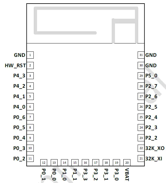
PIN DEFINITIONS
SoC Mode Condition:
Note: INOUT (digital bidirectional), ANA(analog pin), DIG(digital pin
| # | Pin Name | I/O | Ana/Dig | Function |
| 1 | GND | – | GND | GND |
| 2 | HW_RST | IN | DIG | Hardware reset pin; low active; |
| 3 | P4_3 | INOUT | DIG | General purpose IO, 8mA driving capability; With wakeup function, internal strong/weak pull-up and pull-down; |
| 4 | P4_2 | INOUT | DIG | General purpose IO, 8mA driving capability; With wakeup function, internal strong/weak pull-up and pull-down; |
| 5 | P4_1 | INOUT | DIG | General purpose IO, 8mA driving capability; With wakeup function, internal strong/weak pull-up and pull-down; |
| 6 | P4_0 | INOUT | DIG | General purpose IO, 8mA driving capability; With wakeup function, internal strong/weak pull-up and pull-down; |
| 7 | P0_6 | INOUT | DIG | General purpose IO, 8mA driving capability; With wakeup function, internal strong/weak pull-up and pull-down; |
| 8 | P0_5 | INOUT | DIG | General purpose IO, 8mA driving capability; With wakeup function, internal strong/weak pull-up and pull-down; |
| 9 | P0_4 | INOUT | DIG | General purpose IO, 8mA driving capability; With wakeup function, internal strong/weak pull-up and pull-down; |
| 10 | P0_3 | OUT | DIG | LOG_UART_TX (default) |
| 11 | P0_2 | INOUT | DIG | General purpose IO, 8mA driving capability; With wakeup function, internal strong/weak pull-up and pull-down; |
| 12 | P0_1 | INOUT | DIG | General purpose IO, 8mA driving capability; With wakeup function, internal strong/weak pull-up and pull-down; |
| 13 | P0_0 | INOUT | DIG | General purpose IO, 8mA driving capability; With wakeup function, internal strong/weak pull-up and pull-down; |
| 14 | P1_0 | INOUT | DIG | SWDIO (default) General purpose IO, 8mA driving capability; With wakeup function, internal strong/weak pull-up and pull-down; |
| 15 | P1_1 | INOUT | DIG | SWDCLK (default) General purpose IO, 8mA driving capability; With wakeup function, internal strong/weak pull-up and pull-down; |
| 16 | P3_3 | INOUT | DIG | General purpose IO, 8mA driving capability; With wakeup function, internal strong/weak pull-up and pull-down; |
| 17 | P3_2 | INOUT | DIG | General purpose IO, 8mA driving capability; With wakeup function, internal strong/weak pull-up and pull-down; |
| 18 | P3_1 | INOUT | DIG | HCI_UART_RX (default) General purpose IO, 8mA driving capability; With wakeup function, internal strong/weak pull-up and pull-down; |
| 19 | P3_0 | INOUT | DIG | HCI_UART_TX (default) General purpose IO, 8mA driving capability; With wakeup function, internal strong/weak pull-up and pull-down; |
| 20 | VBAT | – | PWR | Power Supply, 1.8V to 3.6V; |
| 21 | 32K_XI | INOUT | ANA/DIG | 32k crystal input or external 32k clock input (optional) Pin share as GPIO when external 32k is not used. |
| 22 | 32K_XO | INOUT | ANA/DIG | 32k crystal output (optional) Pin share as GPIO when external 32k is not used. |
| 23 | P2_2 | INOUT | ANA/DIG | AUXADC input 2 (default) General purpose IO, 8mA driving capability; With wakeup function, internal strong/weak pull-up and pull-down; |
| 24 | P2_3 | INOUT | ANA/DIG | AUXADC input 3 (default) General purpose IO, 8mA driving capability; With wakeup function, internal strong/weak pull-up and pull-down; |
| 25 | P2_4 | INOUT | ANA/DIG | AUXADC input 4 (default) General purpose IO, 8mA driving capability; With wakeup function, internal strong/weak pull-up and pull-down; |
| 26 | P2_5 | INOUT | ANA/DIG | AUXADC input 5 (default) General purpose IO, 8mA driving capability; With wakeup function, internal strong/weak pull-up and pull-down; |
| 27 | P2_6 | INOUT | ANA/DIG | AUXADC input 6 (default) General purpose IO, 8mA driving capability; With wakeup function, internal strong/weak pull-up and pull-down; |
| 28 | P2_7 | INOUT | ANA/DIG | AUXADC input 7 (default) General purpose IO, 8mA driving capability; With wakeup function, internal strong/weak pull-up and pull-down; |
| 29 | P5_0 | INOUT | DIG | General purpose IO, 8mA driving capability; With wakeup function, internal strong/weak pull-up and pull-down; |
| 30 | GND | – | GND | GND |
| 31 | GND | – | GND | GND |
ELECTRICAL CHARACTERISTICS
Temperature Limit Ratings
| Parameter | Description | Note | Min. | Typ. | Max. | Unit |
| TSTORE | Storage temperature | -55 | 125 | °C | ||
| TAOP | Operational Temperature | -30 | 85 | °C |
Power Supply DC Characteristics
| Parameter | Description | Note | Min. | Typ. | Max. | Unit |
| VBAT | Supply Voltage | 1.8 | 3 | 3.6 | V |
ESD Characteristics
| Parameter | Description | Note | Min. | Typ. | Max. | Unit |
| ESDHBM | ESD, human body mode | All pins, test method: JESD22 | 3500 | V | ||
| ESDMM | ESD, machine mode | All pins, test method: JESD22 | 200 | V | ||
| ESDCDM | ESD, charged device mode | All pins, test method: JESD22 | 500 | V |
12bit-AUX ADC Characteristics
| Parameter | Description | Note | Min. | Typ. | Max. | Unit |
| ADCBIT | Resolution | Bypass mode | 12 | BITS | ||
| Divided mode (1/3.3) | 12 | BITS | ||||
| FCLK_ADC | Clock Source | From digital | 400 | kHz | ||
|
ADCDNL |
DNL | Single-ended mode (Bypass mode) | ±1.5 | LSB | ||
| Differential mode (Bypass mode) | ±3.0 | LSB | ||||
|
ADCINL |
INL | Single-ended mode (Bypass mode) | ±1.0 | LSB | ||
| Differential mode (Bypass mode) | ±2.0 | LSB | ||||
|
ADCVIN_RANGE |
Input Voltage Range | External channel (Divided Mode) | 0 | VBAT | V | |
| External channel (Bypass Mode) | 0 | 1 | – | |||
| Internal channel (VBAT) | 1.8 | 3.63 | V | |||
| ADCR_IN | Input Impedance | Bypass mode | 10M | Ohm | ||
| Resistor divider mode (1/4) | 500k | Ohm | ||||
| ADCC_Sample | Input Impedance | Bypass mode | 1.9 | pF | ||
| Resistor divider mode (1/4) | 1.9 | pF |
Radio Characteristics
General Radio Characteristics
| Parameter | Description | Note | Min. | Typ. | Max. | Unit |
| FRANGE | Frequency range | 2402 | 2480 | MHz |
RX Performance
Condition: VBAT=3V, ambient temperature=25°C
| Parameter | Description | Note | Min. | Typ. | Max. | Unit |
| PRX_MIN | Sensitivity (LE 1M) | PER ≤ 30.8% | -97 | dBm | ||
| PRX_MAX | Maximum received power | PER ≤ 30.8% | -1 | dBm | ||
|
CIRX_1M | C/I co-channel | 21 | dB | |||
| C/I + 1MHz offset | 15 | dB | ||||
| C/I – 1MHz offset | 15 | dB | ||||
| C/I + 2MHz offset | -17 | dB | ||||
| C/I – 2MHz offset | -15 | dB | ||||
| C/I + 3MHz offset | -27 | dB | ||||
| C/I image | -9 | dB | ||||
| C/I image + 1MHz offset | -15 | dB | ||||
| C/I image – 1MHz offset | -15 | dB | ||||
|
PRX_OOB | Blocker Power Wanted signal level= – 67dBm | 30MHz ~ 2000MHz | -30 | dBm | ||
| 2003MHz ~ 2399MHz | -30 | dBm | ||||
| 2484MHz ~ 2997MHz | -30 | dBm | ||||
| 3000MHz ~ 12.75GHz | -30 | dBm | ||||
| PERMAX | Max PER report integrity | Wanted signal= -30dBm | 50% | – | ||
|
PRX_IMD |
Max Intermodulation level | Wanted signal f(0) = -64dBm Worst intermodulation level @2f1-f2=f0, |f1-f2|=n MHz, n=3,4,5… |
-50 |
dBm |
TX Performance
Condition: VBAT=3V, ambient temperature=25°C
| Parameter | Description | Note | Min. | Typ. | Max. | Unit |
| PTX_MAX | Maximum output power | 8 | dBm | |||
|
PTX_ADJ | Adjacent channel power ratio (LE 1M) | +2MHz | -20 | dBm | ||
| -2MHz | -20 | dBm | ||||
| ≥ +3MHz | -30 | dBm | ||||
| ≤ -3MHz | -30 | dBm | ||||
|
FMOD |
Modulation Characteristics (LE 1M) | ∆f1avg | 250 | kHz | ||
| ∆f2max | 185 | kHz | ||||
| ∆f2max pass rate | 100% | – | ||||
| ∆f2avg / ∆f1avg | 0.88 | – | ||||
|
FCAR_OFFSET | Carrier frequency offset and drift (LE 1M) | Average Fn | 12.5 | kHz | ||
| Drift rate | 10 | kHz/50ms | ||||
| Average drift | 10 | kHz/50ms | ||||
| Maximum drift | 10 | kHz/50ms | ||||
| PTX_HD2 | 2nd harmonic power | -50 | dBm | |||
| PTX_HD3 | 3rd harmonic power | -50 | dBm |
Digital I/O Pin DC Characteristics
Condition: ambient temperature=25°C
| Parameter | Description | Note | Min. | Typ. | Max. | Unit |
| VIH33 | Input high voltage |
VDDIO=3.3V | 2 | 3.3 | 3.6 | V |
| VIL33 | Input low voltage | 0 | 0.9 | V | ||
| VOH33 | Output high voltage | 2.97 | 3.3 | V | ||
| VOL33 | Output low voltage | 0 | 0.33 | V | ||
| VIH28 | Input high voltage |
VDDIO=2.8V | 1.8 | 2.8 | 3.1 | V |
| VIL28 | Input low voltage | 0 | 0.8 | V | ||
| VOH28 | Output high voltage | 2.5 | V | |||
| VOL28 | Output low voltage | 0 | 0.28 | V | ||
|
Rpull | Strong Pull | VDDIO=3.3V | 10 | kOhm | ||
| VDDIO=1.8V | 20 | kOhm | ||||
| Weak Pull | VDDIO=3.3V | 100 | kOhm | |||
| VDDIO=1.8V | 200 | kOhm | ||||
| Strong Pull (P2_2~P2_7) | VDDIO=3.3V | 5 | kOhm | |||
| VDDIO=1.8V | 2.5 | kOhm |
| Rpull | Weak Pull (P2_2~P2_7) | VDDIO=3.3V | 50 | kOhm | ||
| VDDIO=1.8V | 25 | kOhm | ||||
| IIH | Input high current | PAD configured as input mode | 0.1 | mA | ||
| IIL | Input low current | 0.1 | mA |
Boot Sequence
Boot up by internal power on reset circuit, power on timing is shown in below figure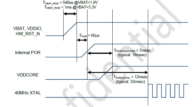
Boot up by HW_RST_N pin, power on timing is shown in below figure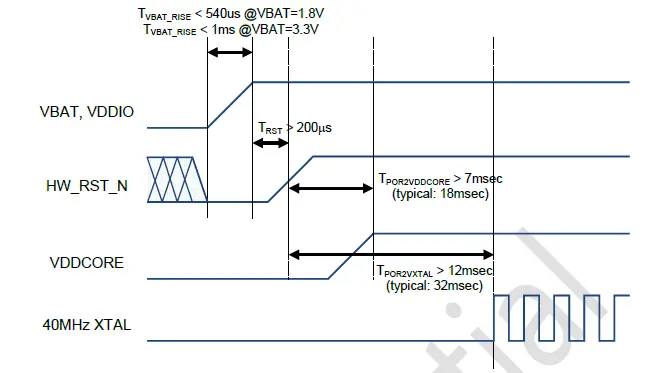
UART Characteristics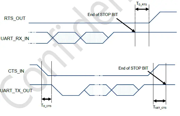
| Parameter | Description | Note | Min. | Typ. | Max. | Unit |
| TD_RTS | Timing between UART_RX_IN stop bit and RTS rising edge when RX FIFO is full | 0.5 | ns | |||
| TD_CTS | Timing between CTS falling edge and UART_TX_OUT first bit | 25 | ns |
| TSET_CTS | Timing between CTS rising edge and UART_TX_OUT stop bit | 75 | ns |
PCB LAYOUT GUIDE
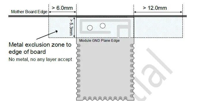
Module Placement Example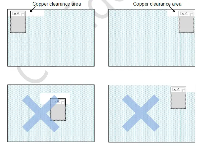
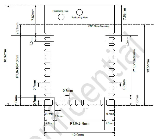
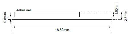
MODULE DIMENSIONS

Federal Communication Commission Interference Statement
This device complies with Part 15 of the FCC Rules. Operation is subject to the following two conditions:
- this device may not cause harmful interference
- this device must accept any interference received, including interference that may cause undesired operation.
RF Exposure warning
This equipment must be installed and operated in accordance with provided instructions and the antenna(s) used for this transmitter must be installed to provide a separation distance of at least 20 cm from all persons and must not be co-located or operating in conjunction with any other antenna or transmitter. End-users and installers must be provide with antenna installation instructions and transmitter operating conditions for satisfying RF exposure compliance.
AUTION:
Any changes or modifications not expressly approved by the grantee of this device could void the user’s authority to operate the equipment.
End Product Labeling
This transmitter module is authorized only for use in device where the antenna may be installed such that 20cm may be maintained between the antenna and users. The final end product must be labeled in a visible area with the following: “Contains FCC ID: 2AXKL-BTRT6MB”.
Information for the OEMs and Integrators
The following statement must be included with all versions of this document supplied to an OEM or integrator, but should not be distributed to the end user.
- This device is intended for OEM integrators only.
- Please see the full Grant of Equipment document for other restrictions.
Vital-Tech Electronics Limited Corporation & MediaWave Intelligent Communication LTD.
VT-RT6MB BLE Module User Manual, Version 0.2beta
Copyright © 2022 Vital Tech Electronics Limited. All rights reserved.


