intel UG-20094 Cyclone 10 GX Native Fixed Point DSP IP Core
Intel® Cyclone® 10 GX Native Fixed Point DSP IP Core User Guide
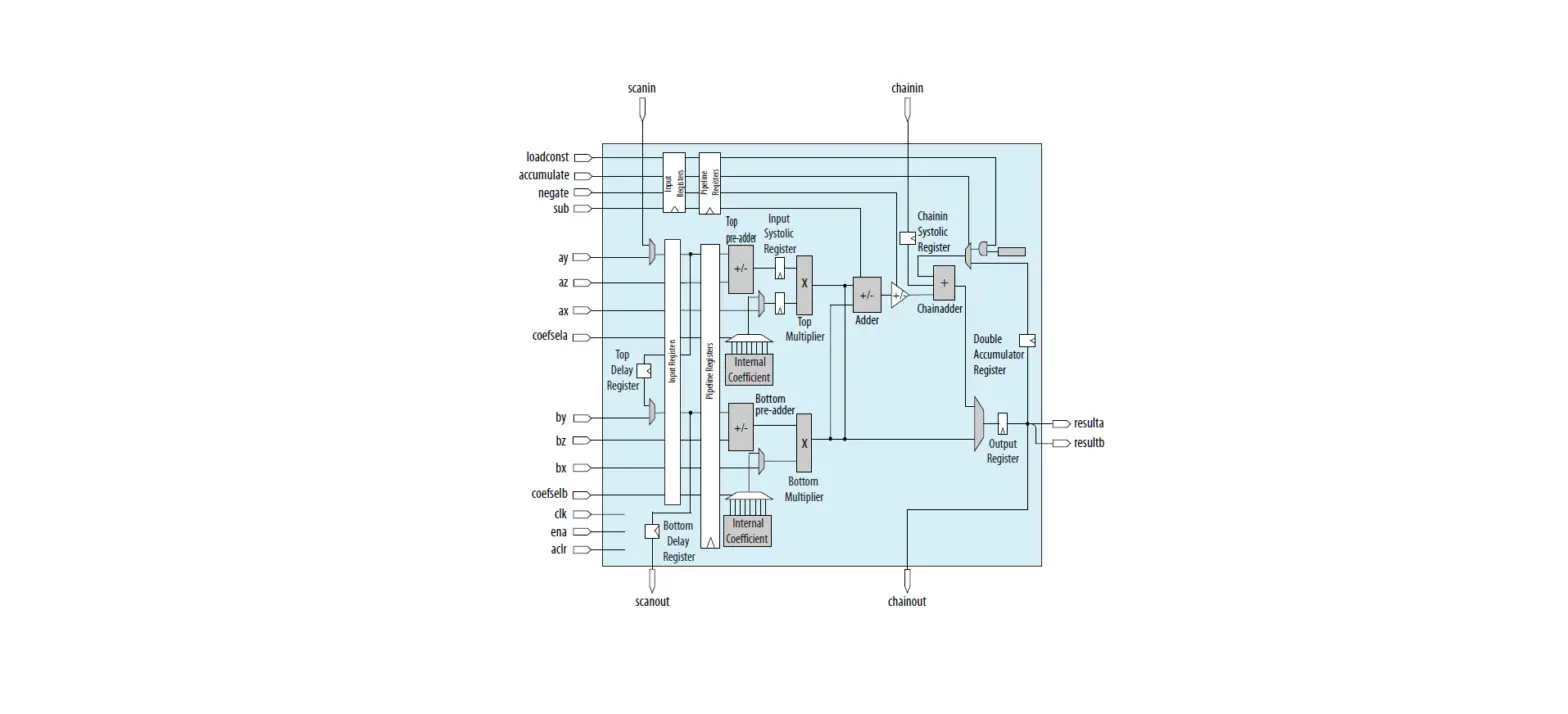
The Intel Cyclone® 10 GX Native Fixed Point DSP IP core instantiates and controls a single Intel Cyclone 10 GX Variable Precision Digital Signal Processing (DSP) block. The Cyclone 10 GX Native Fixed Point DSP IP core is only available for Intel Cyclone 10 GX devices.
Cyclone 10 GX Native Fixed Point DSP IP Core Functional Block Diagram
Related Information
Introduction to Intel FPGA IP Cores.
Cyclone 10 GX Native Fixed Point DSP IP Core Features
The Cyclone 10 GX Native Fixed Point DSP IP core supports the following features:
- High-performance, power-optimized, and fully registered multiplication operations
- 18-bit and 27-bit word lengths
- Two 18 × 19 multipliers or one 27 × 27 multiplier per DSP block
- Built-in addition, subtraction, and 64-bit double accumulation register to combine multiplication results
- Cascading 19-bit or 27-bit when pre-adder is disabled and cascading 18-bit when pre-adder is used to form the tap-delay line for filtering application
- Cascading 64-bit output bus to propagate output results from one block to the next block without external logic support
- Hard pre-adder supported in 19-bit and 27-bit modes for symmetric filters
- Internal coefficient register bank in both 18-bit and 27-bit modes for filter implementation
- 18-bit and 27-bit systolic finite impulse response (FIR) filters with distributed output adder
Getting Started
This chapter provides a general overview of the Intel FPGA IP core design flow to help you quickly get started with the Cyclone 10 GX Native Fixed Point DSP IP core. The Intel FPGA IP Library is installed as part of the Intel Quartus® Prime installation process. You can select and parameterize any Intel FPGA IP core from the library. Intel provides an integrated parameter editor that allows you to customize the Intel FPGA DSP IP core to support a wide variety of applications. The parameter editor guides you through the setting of parameter values and the selection of optional ports.
Related Information
- Introduction to Intel FPGA IP Cores
Provides general information about all Intel FPGA IP cores, including parameterizing, generating, upgrading, and simulating IP cores. - Creating Version-Independent IP and Platform Designer (Standard) Simulatio Scripts
Create simulation scripts that do not require manual updates for software or IP version upgrades. - Project Management Best Practices
Guidelines for efficient management and portability of your project and IP files.
Cyclone 10 GX Native Fixed Point DSP IP Core Parameter Settings
You can customize the Cyclone 10 GX Native Fixed Point DSP IP core by specifying the parameters using the parameter editor in the Intel Quartus Prime software.
Operation Mode Tab
| Parameter | IP Generated Parameter | Value | Description |
| Please choose the operation mode | operation_mode | m18×18_full m18×18_sumof2 m18×18_plus36 m18×18_systolic m27×27 | Select the desired operational mode. |
| Multiplier Configuration | |||
| Representation format for top multiplier x operand | signed_max | signed unsigned | Specify the representation format for the top multiplier x operand. |
| Parameter | IP Generated Parameter | Value | Description |
| Representation format for top multiplier y operand | signed_may | signed unsigned | Specify the representation format for the top multiplier y operand. |
| Representation format for bottom multiplier x operand | signed_mbx | signed unsigned | Specify the representation format for the bottom multiplier x operand. |
| Representation format for bottom multiplier y operand | signed_mby | signed unsigned | Specify the representation format for the bottom multiplier y operand. Always select unsigned for m18×18_plus36 . |
| Enable ‘sub’ port | enable_sub | No Yes | Select Yes to enable sub port. |
| Register input ‘sub’ of the multiplier | sub_clock | No Clock0 Clock1 Clock2 | Select Clock0, Clock1, or Clock2 to enable and specify the input clock signal for sub input register. |
| Input Cascade | |||
| Enable input cascade for ‘ay’ input | ay_use_scan_in | No Yes | Select Yes to enable input cascade module for ay data input. When you enable input cascade module, the Cyclone 10 GX Native Fixed Point DSP IP core uses the scanin input signals as input instead of ay input signals. |
| Enable input cascade for ‘by’ input | by_use_scan_in | No Yes | Select Yes to enable input cascade module for by data input. When you enable input cascade module, the Cyclone 10 GX Native Fixed Point DSP IP core uses the ay input signals as input instead of by input signals. |
| Enable data ay delay register | delay_scan_out_ay | No Yes | Select Yes to enable delay register between ay and by input registers. This feature is not supported in m18×18_plus36 and m27x27 operational mode. |
| Parameter | IP Generated Parameter | Value | Description |
| Enable data by delay register | delay_scan_out_by | No Yes | Select Yes to enable delay register between by input registers and scanout output bus. This feature is not supported in m18×18_plus36 and m27x27 operational mode. |
| Enable scanout port | gui_scanout_enable | No Yes | Select Yes to enable scanout output bus. |
| ‘scanout’ output bus width | scan_out_width | 1–27 | Specify the width of scanout output bus. |
| Data ‘x’ Configuration | |||
| ‘ax’ input bus width | ax_width | 1–27 | Specify the width of ax input bus.(1) |
| Register input ‘ax’ of the multiplier | ax_clock | No Clock0 Clock1 Clock2 | Select Clock0, Clock1, or Clock2 to enable and specify the input clock signal for ax input register. ax input register is not available if you set ‘ax’ operand source to ‘coef’. |
| ‘bx’ input bus width | bx_width | 1–18 | Specify the width of bx input bus.(1) |
| Register input ‘bx’ of the multiplier | bx_clock | No Clock0 Clock1 Clock2 | Select Clock0, Clock1, or Clock2 to enable and specify the input clock signal for bx input register. bx input register is not available if you set ‘bx’ operand source to ‘coef’. |
| Data ‘y’ Configuration | |||
| ‘ay’ or ‘scanin’ bus width | ay_scan_in_width | 1–27 | Specify the width of ay or scanin input bus.(1) |
| Register input ‘ay’ or input ‘scanin’ of the multiplier | ay_scan_in_clock | No Clock0 Clock1 Clock2 | Select Clock0, Clock1, or Clock2 to enable and specify the input clock signal for ay or scanin input register. |
| ‘by’ input bus width | by_width | 1–19 | Specify the width of by input bus.(1) |
| Parameter | IP Generated Parameter | Value | Description |
| Register input ‘by’ of the multiplier | by_clock | No Clock0 Clock1 Clock2 | Select Clock0, Clock1, or Clock2 to enable and specify the input clock signal for by or scanin input register.(1) |
| Output ‘result’ Configuration | |||
| ‘resulta’ output bus width | result_a_width | 1–64 | Specify the width of resulta output bus. |
| ‘resultb’ output bus width | result_b_width | 1–64 | Specify the width of resultb output bus. resultb only available when using operation_mode m18×18_full. |
| Use output register | output_clock | No Clock0 Clock1 Clock2 | Select Clock0, Clock1, or Clock2 to enable and specify the input clock signal for resulta and resultb output registers. |
Pre-adder Tab
| Parameter | IP Generated Parameter | Value | Description |
| ‘ay’ operand source | operand_source_may | input preadder | Specify the operand source for ay input. Select preadder to enable pre-adder module for top multiplier. Settings for ay and by operand source must be the same. |
| ‘by’ operand source | operand_source_mby | input preadder | Specify the operand source for by input. Select preadder to enable pre-adder module for bottom multiplier. Settings for ay and by operand source must be the same. |
| Set pre-adder a operation to subtraction | preadder_subtract_a | No Yes | Select Yes to specify subtraction operation for pre-adder module for the top multiplier. Pre-adder settings for top and bottom multiplier must be the same. |
| Set pre-adder b operation to subtraction | preadder_subtract_b | No Yes | Select Yes to specify subtraction operation for pre-adder module for the bottom multiplier. Pre-adder settings for top and bottom multiplier must be the same. |
| Data ‘z’ Configuration | |||
| ‘az’ input bus width | az_width | 1–26 | Specify the width of az input bus.(1) |
| Register input ‘az’ of the multiplier | az_clock | No Clock0 Clock1 Clock2 | Select Clock0, Clock1, or Clock2 to enable and specify the input clock signal for az input registers. Clock settings for ay and az input registers must be the same. |
| ‘bz’ input bus width | bz_width | 1–18 | Specify the width of bz input bus.(1) |
| Register input ‘bz’ of the multiplier | bz_clock | No Clock0 Clock1 Clock2 | Select Clock0, Clock1, or Clock2 to enable and specify the input clock signal for bz input registers. Clock settings for by and bz input registers must be the same. |
Internal Coefficient Tab
| Parameter | IP Generated Parameter | Value | Description |
| ‘ax’ operand source | operand_source_max | input coef | Specify the operand source for ax input bus. Select coef to enable internal coefficient module for top multiplier. Select No for Register input ‘ax’ of the multiplier parameter when you enable the internal coefficient feature. |
| Parameter | IP Generated Parameter | Value | Description |
| Settings for ax and bx operand source must be the same. | |||
| ‘bx’ operand source | operand_source_mbx | input coef | Specify the operand source for bx input bus. Select coef to enable internal coefficient module for top multiplier. Select No for Register input ‘bx’ of the multiplier parameter when you enable the internal coefficient feature. Settings for ax and bx operand source must be the same. |
| ‘coefsel’ Input Register Configuration | |||
| Register input ‘coefsela’ of the multiplier | coef_sel_a_clock | No Clock0 Clock1 Clock2 | Select Clock0, Clock1, or Clock2 to enable and specify the input clock signal for the coefsela input registers. |
| Register input ‘coefselb’ of the multiplier | coef_sel_b_clock | No Clock0 Clock1 Clock2 | Select Clock0, Clock1, or Clock2 to enable and specify the input clock signal for the coefselb input registers. |
| Coefficient Storage Configuration | |||
| coef_a_0–7 | coef_a_0–7 | Integer | Specify the coefficient values for ax input bus. For 18-bit operation mode, the maximum input value is 218 – 1. For 27-bit operation, the maximum value is 227 – 1. |
| coef_b_0–7 | coef_b_0–7 | Integer | Specify the coefficient values for bx input bus. |
Accumulator/Output Cascade Tab
| Parameter | IP Generated Parameter | Value | Description |
| Enable ‘accumulate’ port | enable_accumulate | No Yes | Select Yes to enable accumulator port. |
| Enable ‘negate’ port | enable_negate | No Yes | Select Yes to enable negate port. |
| Enable ‘loadconst’ port | enable_loadconst | No Yes | Select Yes to enable loadconst port. |
| Register input ‘accumulate’ of the accumulator | accumulate_clock | No Clock0 Clock1 Clock2 | Select Clock0 , Clock1, or Clock2 to enable and specify the input clock signal for the accumulate input registers. |
| Parameter | IP Generated Parameter | Value | Description |
| Register input ‘loadconst’ of the accumulator | load_const_clock | No Clock0 Clock1 Clock2 | Select Clock0, Clock1, or Clock2 to enable and specify the input clock signal for the loadconst input registers. |
| Register input ‘negate’ of the adder unit | negate_clock | No Clock0 Clock1 Clock2 | Select Clock0, Clock1, or Clock2 to enable and specify the input clock signal for the negate input registers. |
| Enable double accumulator | enable_double_accum | No Yes | Select Yes to enable double accumulator feature. |
| N value of preset constant | load_const_value | 0 – 63 | Specify the preset constant value. This value can be 2N where N is the preset constant value. |
| Enable chainin port | use_chainadder | No Yes | Select Yes to enable output cascade module and the chainin input bus. Output cascade feature is not supported in m18×18_full operation mode. |
| Enable chainout port | gui_chainout_enable | No Yes | Select Yes to enable the chainout output bus. Output cascade feature is not supported in m18×18_full operation mode. |
Pipelining Tab
| Parameter | IP Generated Parameter | Value | Description |
| Add input pipeline register to the input data signal (x/y/z/coefsel) | input_pipeline_clock | No Clock0 Clock1 Clock2 | Select Clock0, Clock1, or Clock2 to enable and specify the input clock signal for x, y, z, coefsela and coefselb pipeline input registers. |
| Add input pipeline register to the ‘sub’ data signal | sub_pipeline_clock | No Clock0 Clock1 Clock2 | Select Clock0, Clock1, or Clock2 to enable and specify the input clock signal for the sub pipeline input register. (2) |
| Add input pipeline register to the ‘accumulate’ data signal | accum_pipeline_clock | No Clock0 Clock1 Clock2 | Select Clock0, Clock1, or Clock2 to enable and specify the input clock signal for the accumulate pipeline input register.(2) |
| Add input pipeline register to the ‘loadconst’ data signal | load_const_pipeline_clock | No Clock0 Clock1 Clock2 | Select Clock0, Clock1, or Clock2 to enable and specify the input clock signal for the loadconst pipeline input register.(2) |
| Add input pipeline register to the ‘negate’ data signal | negate_pipeline_clock | No Clock0 Clock1 Clock2 | Select Clock0, Clock1, or Clock2 to enable and specify the input clock signal for the negate pipeline input register.(2) |
Maximum Input Data Width Per Operation Mode
You can customize the data width for x, y, and z inputs as specified in the table.
All pipeline input registers for dynamic control signals must have the same clock setting.
| Operation Mode | Maximum Input Data Width | |||||
| ax | ay | az | bx | by | bz | |
| Without Pre-adder or Internal Coefficient | ||||||
| m18×18_full | 18 (signed) 18 (unsigned) | 19 (signed) 18 (unsigned) | Not used | 18 (signed) 18 (unsigned) | 19 (signed) 18 (unsigned) | Not used |
| m18×18_sumof2 | ||||||
| m18×18_systolic | ||||||
| m18×18_plus36 | ||||||
| m27×27 | 27 (signed) 27 (unsigned) | Not used | ||||
| With Pre-adder Feature Only | ||||||
| m18×18_full | 18 (signed) 18 (unsigned) | |||||
| m18×18_sumof2 | ||||||
| m18×18_systolic | ||||||
| m27×27 | 27 (signed) 27 (unsigned) | 26 (signed) 26 (unsigned) | Not used | |||
| With Internal Coefficient Feature Only | ||||||
| m18×18_full | Not used | 19 (signed) 18 (unsigned) | Not used | 19 (signed) 18 (unsigned) | Not used | |
| m18×18_sumof2 | ||||||
| m18×18_systolic | ||||||
| m27×27 | 27 (signed) 27 (unsigned) | Not used | ||||
Functional Description
The Cyclone 10 GX Native Fixed Point DSP IP core consists of 2 architectures; 18 × 18 multiplication and 27 × 27 multiplication. Each instantiation of the Cyclone 10 GX Native Fixed Point DSP IP core generates only 1 of the 2 architectures depending on the selected operational modes. You can enable optional modules to your application.
Related Information
Variable Precision DSP Blocks in Intel Cyclone 10 GX Devices chapter, Intel Cyclone 10 GX Core Fabric and General Purpose I/Os Handbook.
Operational Modes
The Cyclone 10 GX Native Fixed Point DSP IP core supports 5 operational modes:
- The 18 × 18 Full Mode
- The 18 × 18 Sum of 2 Mode
- The 18 × 18 Plus 36 Mode
- The 18 × 18 Systolic Mode
- The 27 × 27 Mode
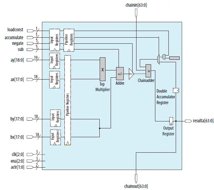
The 18 × 18 Full Mode
When configured as 18 × 18 full mode, the Cyclone 10 GX Native Fixed Point DSP IP core operates as two independent 18 (signed/unsigned) × 19 (signed) or 18
(signed/unsigned) × 18 (unsigned) multipliers with 37-bit output. This mode applies the following equations:
- resulta = ax * ay
- resultb = bx * by
The 18 × 18 Full Mode Architecture
The 18 × 18 Sum of 2 Mode
In 18 × 18 Sum of 2 modes, the Cyclone 10 GX Native Fixed Point DSP IP core enables the top and bottom multipliers and generates a result from addition or subtraction between the 2 multipliers. The sub-dynamic control signal controls an adder to perform the addition or subtraction operations. The resulta output width of the Cyclone 10 GX Native Fixed Point DSP IP core can support up to 64 bits when you enable accumulator/output cascade. This mode applies the equation of resulta =[±(ax * ay) + (bx * by)].
The 18 × 18 Sum of 2 Mode Architecture
The 18 × 18 Plus 36 Mode
When configured as 18 × 18 Plus 36 mode, the Cyclone 10 GX Native Fixed Point DSP IP core enables only the top multiplier. This mode applies the equation of resulta = (ax * ay) + concatenate(bx[17:0],by[17:0]).
The 18 × 18 Plus 36 Mode Architecture
You must set the Representation format for bottom multipliers y operand to unsigned when using this mode. When the input bus is less than 36-bit in this mode, you are required to provide the necessary signed extension to fill up the 36-bit input.
Using Less Than 36-bit Operand In 18 × 18 Plus 36 Mode
This example shows how to configure the Cyclone 10 GX Native Fixed Point DSP IP core to use 18 × 18 Plus 36 operational mode with a signed 12-bit input data of 101010101010 (binary) instead of a 36-bit operand.
- Set Representation format for bottom multiplier x operand: to signed.
- Set Representation format for bottom multiplier y operand: to unsigned.
- Set ‘bx’ input bus width to 18.
- Set ‘by’ input bus width to 18.
- Provide data of ‘111111111111111111’ to bx input bus.
- Provide data of ‘111111101010101010’ to by input bus.
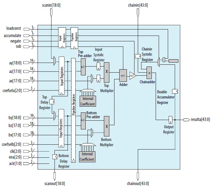
The 18 × 18 Systolic Mode
In 18 × 18 systolic operational modes, the Cyclone 10 GX Native Fixed Point DSP IP core enables the top and bottom multipliers, an input systolic register for the top multiplier, and a chain systolic register for the chain in input signals. When you enable output cascade, this mode supports resulta output width of 44 bits. When you enable the accumulator feature without output cascade, you can configure the resulta output width to 64 bits.
The 18 × 18 Systolic Mode Architecture
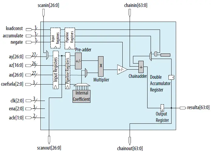
The 27 × 27 Mode
When configured as 27 × 27 modes, the Cyclone 10 GX Native Fixed Point DSP IP core enables a 27(signed/unsigned) × 27(signed/unsigned) multiplier. The output bus can support up to 64 bits with accumulator/output cascade enabled. This mode applies the equation of resulta = ax * ay.
The 27 × 27 Mode Architecture
Optional Modules
The optional modules available in the Cyclone 10 GX Native Fixed Point DSP IP Core are:
- Input cascade
- Pre-adders
- Internal Coefficient
- Accumulator and output cascade
- Pipeline registers
Input Cascade
Input cascade feature is supported on ay and by input bus. When you set Enable input cascade for ‘ay’ input to Yes, the Cyclone 10 GX Native Fixed Point DSP IP core will take inputs from scan input signals instead of ay input bus. When you set Enable input cascade for ‘by’ input to Yes, the Cyclone 10 GX Native Fixed Point DSP IP core will take inputs from ay input bus instead of by input bus.
It is recommended to enable the input registers for ay and/or by whenever input cascade is enabled for the correctness of the application.
You can enable the delay registers to match the latency requirement between the input register and the output register. There are 2 delay registers in the core. The top delay register is used for ay or scan-in input ports while the bottom delay register is used for scanout output ports. These delay registers are supported in 18 × 18 full mode, 18 × 18 sums of 2 modes, and 18 × 18 systolic modes.
Pre-adder
The pre-adder can be configured in the following configurations:
- Two independent 18-bit (signed/unsigned) pre-adders.
- One 26-bit pre-adder.
When you enable pre-adder in 18 × 18 multiplication modes, ay and az are used as the input bus to the top pre-adder while by and bz are used as the input bus to the bottom pre-adder. When you enable pre-adder in 27 × 27 multiplication mode, ay and az are used as the input bus to the pre-adder. The pre-adder supports both addition and subtraction operations. When both pre-adders within the same DSP block are used, they must share the same operation type (either addition or subtraction).
Internal Coefficient
The internal coefficient can support up to eight constant coefficients for the multiplicands in 18-bit and 27-bit modes. When you enable the internal coefficient feature, two input buses to control the selection of the coefficient multiplexer will be generated. The coefsela input bus is used to select the predefined coefficients for the top multiplier and the counsel input bus is used to select the predefined coefficients for the bottom multiplier.
The internal coefficient storage does not support dynamically controllable coefficient values and external coefficient storage is required to perform such an operation.
Accumulator and Output Cascade
The accumulator module can be enabled to perform the following operations:
- Addition or subtraction operation
- Biased rounding operation using a constant value of 2N
- Dual channel accumulation
To dynamically perform addition or subtraction operation of the accumulator, control the negate input signal. For a biased rounding operation, you can specify and load a preset constant of 2N before the accumulator module is enabled by specifying an integer to the parameter N value of the preset constant. The integer N must be less than 64. You can dynamically enable or disable the use of the preset constant by controlling the loadconst signal. You can use this operation as an active muxing of the round value into the accumulator feedback path. The loaded cost and the accumulated signal usage is mutually exclusive.
You can enable the double accumulator register using the parameter Enable double accumulator to perform double accumulation. The accumulator module can support the chaining of multiple DSP blocks for addition or subtraction operations by enabling the chaining input port and chain-out output port. In 18 × 18 systolic mode, only 44-bit of the chain input bus and chain out output bus will be used. However, all 64-bit chains in the input bus must be connected to the chain-out output bus from the preceding DSP block.
Pipeline Register
The Cyclone 10 GX Native Fixed Point DSP IP core supports a single level of pipeline register. The pipeline register supports up to three clock sources and one asynchronous clear signal to reset the pipeline registers. There are five pipeline registers:
- data input bus pipeline register
- sub dynamic control signal pipeline register
- negate dynamic control signal pipeline register
- accumulate dynamic control signal pipeline register
- loadconst dynamic control pipeline register
You can choose to enable each data input bus pipeline registers and the dynamic control signal pipeline registers independently. However, all enabled pipeline registers must use the same clock source.
Clocking Scheme
The input, pipeline, and output registers in the Cyclone 10 GX Native Fixed Point DSP IP core supports three clock sources/enables and two asynchronous clears. All input registers use aclr[0] and all pipeline and output registers use aclr[1]. Each register type can select one of the three clock sources and clock enable signals. When you configure the Cyclone 10 GX Native Fixed Point DSP IP core to 18 × 18 systolic operation mode, the Intel Quartus Prime software will set the input systolic register and the chain systolic register clock source to the same clock source as the output register internally.
When you enable the double accumulator feature, the Intel Quartus Prime software will set the double accumulator register clock source to the same clock source as the output register internally.
Clocking Scheme Constraints
This tab shows the constraints you must apply for all the register clocking schemes.
| Condition | Constraint |
| When pre-adder is enabled | Clock source for ay and az input registers must be the same. |
| Clock source for by and bz input registers must be the same. | |
| When pipeline registers are enabled | Clock source for all pipeline registers must be the same. |
| When any of the input registers for dynamic control signals | Clock source for input registers for sub, accumulate, loadconst, and negate must be the same. |
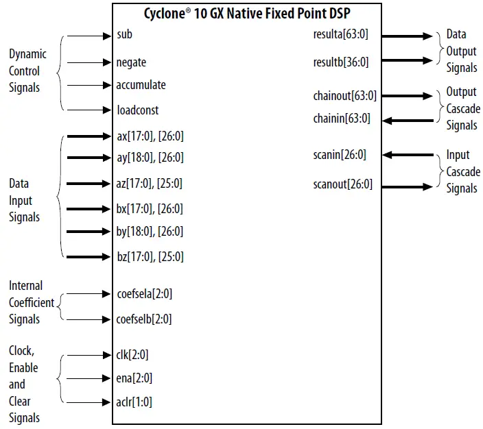
Cyclone 10 GX Native Fixed Point DSP IP Core Signals
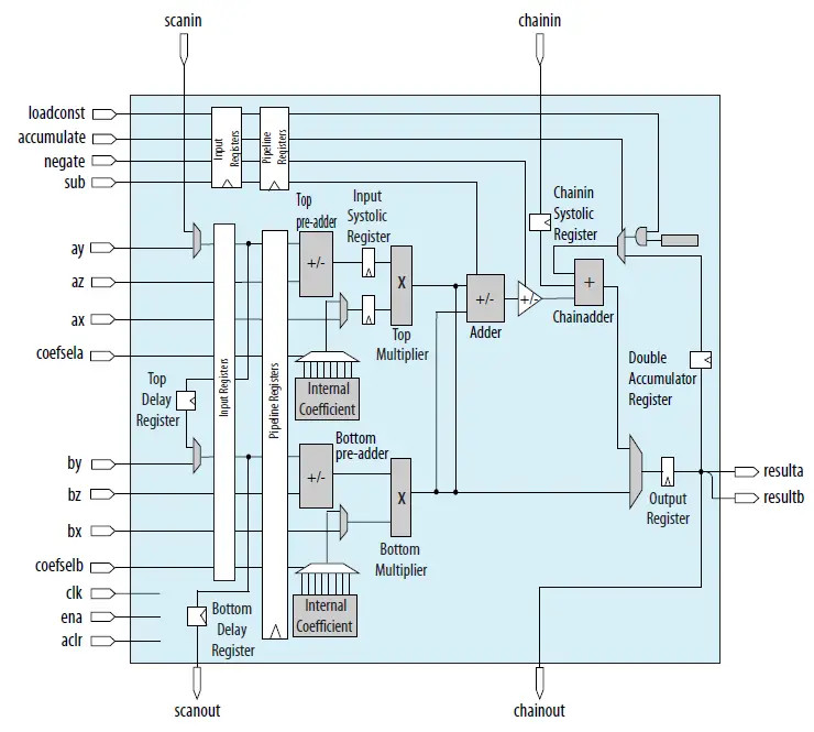
The following figure shows the input and output signals of the Cyclone 10 GX Native Fixed Point DSP IP core.
Cyclone 10 GX Native Fixed Point DSP IP Core Signals
Data Input Signals
| Signal Name | Type | Width | Description |
| ax[] | Input | 27 | Input data bus to top multiplier. |
| ay[] | Input | 27 | Input data bus to top multiplier. When pre-adder is enabled, these signals are served as input signals to the top pre-adder. |
| az[] | Input | 26 | These signals are input signals to the top pre-adder. These signals are only available when pre-adder is enabled. These signals are not available in m18×18_plus36 operational mode. |
| bx[] | Input | 18 | Input data bus to bottom multiplier. These signals are not available in m27×27 operational mode. |
| by[] | Input | 19 | Input data bus to bottom multiplier. When pre-adder is enabled, these signals serve as input signals to the bottom pre-adder. These signals are not available in m27×27 operational mode. |
| bz[] | Input | 18 | These signals are input signals to the bottom pre-adder. These signals are only available when pre-adder is enabled. These signals are not available in m27×27 and m18×18_plus36 operational modes. |
Data Output Signals
| Signal Name | Type | Width | Decsription |
| resulta[] | Output | 64 | Output data bus from top multiplier. These signals support up to 37 bits for m18×18_full operational mode. |
| resultb[] | Output | 37 | Output data bus from bottom multiplier. These signals only available in m18×18_full operational mode. |
Clock, Enable, and Clear Signals
| Signal Name | Type | Width | Description |
| clk[] | Input | 3 | Input clock signals for all registers. These clock signals are only available if any of the input registers, pipeline registers, or output register is set to Clock0, Clock1, or Clock2. • clk[0] = Clock0 • clk[1] = Clock1 • clk[2] = Clock2 |
| ena[] | Input | 3 | Clock enable for clk[2:0]. This signal is active-High. • ena[0] is for Clock0 • ena[1] is for Clock1 • ena[2] is for Clock2 |
| aclr[] | Input | 2 | Asynchronous clear input signals for all registers. This signal is active-High. Use aclr[0] for all input registers and use aclr[1] for all pipeline registers and output register. By default, this signal is de-asserted. |
Dynamic Control Signals
| Signal Name | Type | Width | Description |
| sub | Input | 1 | Input signal to add or subtract the output of the top multiplier with the output of the bottom multiplier. • Deassert this signal to specify addition operation. • Assert this signal to specify subtraction operation. By default, this signal is deasserted. You can assert or deassert this signal during run-time.(3) |
| negate | Input | 1 | Input signal to add or subtract the sum of top and bottom multipliers with the data from chainin signals. • Deassert this signal to specify addition operation. • Assert this signal to specify subtraction operation. By default, this signal is deasserted. You can assert or deassert this signal during run-time.(3) |
| accumulate | Input | 1 | Input signal to enable or disable the accumulator feature. • Deassert this signal to disable the accumulator feature. • Assert this signal to enable the accumulator feature. By default, this signal is deasserted. You can assert or deassert this signal during run-time.(3) |
| loadconst | Input | 1 | Input signal to enable or disable the load constant feature. • Deassert this signal to disable the load constant feature. • Assert this signal to enable the load constant feature. By default, this signal is deasserted. You can assert or deassert this signal during run-time.(3) |
Internal Coeficient Signals
| Signal Name | Type | Width | Description |
| coefsela[] | Input | 3 | Input selection signals for 8 coefficient values defined by user for the top multiplier. The coefficient values are stored in the internal memory and specified by parameters coef_a_0 to coef_a_7. • coefsela[2:0] = 000 refers to coef_a_0 • coefsela[2:0] = 001 refers to coef_a_1 • coelsela[2:0] = 010 refers to coef_a_2 • … and so forth. These signals are only available when the internal coefficient feature is enabled. |
| coefselb[] | Input | 3 | Input selection signals for 8 coefficient values defined by user for the bottom multiplier. The coefficient values are stored in the internal memory and specified by parameters coef_b_0 to coef_b_7. • coefselb[2:0] = 000 refers to coef_b_0 • coefselb[2:0] = 001 refers to coef_b_1 • coelselb[2:0] = 010 refers to coef_b_2 • … and so forth. These signals are only available when the internal coefficient feature is enabled. |
Input Cascade Signals
| Signal Name | Type | Width | Description |
| scanin[] | Input | 27 | Input data bus for input cascade module. Connect these signals to the scanout signals from the preceding DSP core. |
| scanout[] | Ouput | 27 | Output data bus of the input cascade module. Connect these signals to the scanin signals of the next DSP core. |
Output Cascade Signals
| Signal Name | Type | Width | Description |
| chainin[] | Input | 64 | Input data bus for output cascade module. Connect these signals to the chainout signals from the preceding DSP core. |
| chainout[] | Output | 64 | Output data bus of the output cascade module. Connect these signals to the chainin signals of the next DSP core. |
Document Revision History for the Cyclone 10 GX Native Fixed Point DSP IP Core User Guide
| Date | Version | Changes |
| November 2017 | 2017.11.06 | Initial release. |
Intel Corporation. All rights reserved. Intel, the Intel logo, and other Intel marks are trademarks of Intel Corporation or its subsidiaries. Intel warrants the performance of its FPGA and semiconductor products to current specifications in accordance with Intel’s standard warranty but reserves the right to make changes to any products and services at any time without notice. Intel assumes no responsibility or liability arising out of the application or use of any information, product, or service described herein except as expressly agreed to in writing by Intel. Intel customers are advised to obtain the latest version of device specifications before relying on any published information and before placing orders for products or services.
Other names and brands may be claimed as the property of others.


 Agilex Fpga Ip Design Example User Guide")


