RF-star RF-BM-ND06 Bluetooth 5.0 Module
Device Overview
Description
RF-BM-ND06an RF module based on Nordic Bluetooth 5.0 BLE SoC nRF52840-QIAA-R with best-in-class 32-bit ARM® Cortex®-M4 processor. It integrates a 32.768 kHz and a 32 MHz crystal, a power filter, an antenna matching, and a meander line inverted-F PCB antenna. It features high-performance digital interfaces, robust connection distance, and rigid reliability. It supports BLE stack v5.0 and can be preprogrammed with a serial interface communication protocol for simple programming. 1.27-mm pitch stamp stick package for easy assembling and cost-effective PCB design. All pins of RF-BM-ND06 are pulled out.
Key Features
- Bluetooth 5.0,
- -95 dBm conductive sensitivity in BLE mode
- -103 dBm sensitivity in 125kbps BLE mode (long range)
- On-air compatible with nRF52, nRF51, nRF24L and nRF24AP series
- Supported data rates:
Bluetooth ® 5: 2 Mbps, 1Mbps, 500kbps and 125 kbps - Single-ended antenna output (on-chip balun)
- 128-bit AES/ECB/CCM/AAR co-processor (on-the-fly packet encryption)
- 4.8 mA peak current in TX (0 dBm)
- 4.6 mA peak current in RX
- RSSI (1 dB resolution)
- ARM® Cortex®-M4 32-bit processor with FPU, 64 MHz
- 212 EEMBC Core Mark score running from flash memory
- 52 μA/MHz running from flash memory
- Watch point and trace debug modules (DWT, ETM and ITM)
- Serial wire debug (SWD)
- Rich set of security features
- ARM®Trust Zone®Cryptocell 310 security subsystem
- Security boot ready
- Secure erase
- Flexible power management
- Supply voltage range: 1.8 V ~ 5.5 V
- Automated peripheral power management
- Fast wake-up using 64 MHz internal oscillator
- 0.4 μA at 3 V in System OFF mode, no RAM retention
- 1.5 μA at 3 V in System On mode, no RAM retention, wake on RTC
- 1 MB flash and 256 kB RAM
- Advanced on-chip interfaces
- QSPI 32 MHz interface
- High-speed 32 MHz SPI
- Type 2 near field communication (NFC-A) tag with wake-on field
Touch-to-pair support - Programmable Peripheral interconnect (PPI)
- 29 general purpose I/O pins
- Easy DMA automated data transfer between memory and peripherals
- Nordic Soft Device ready with support for concurrent multi-protocol
- 12-bit, 200 ksps ADC – 8 configurable channels with programmable gain
- 64 level comparator
- 15 level low-power comparator with wake-up from System OFF mode
- Temperature sensor
- 4x 4-channel pulse width modulator (PWM) unit with EasyDMA
- Audio peripherals: I2S, digital microphone interface (PDM)
- 5x 32-bit timer with counter mode
- Up to 4xSPI master/3x SPI slave with EasyDMA
- Up to 2x I2C compatible 2-wire master/slave
- 2xUART (CTS/RTS) with EasyDMA
- Quadrature decoder (QDEC)
- 3xreal-time counter (RTC)
Applications
- Internet of Things (IoT)
- Internet Gateway
- Cloud Connectivity
- Industrial Control
- Home Automation
- Smart Plug and Metering
- Home Appliances
- Wireless Audio
- Access Control
- IP Network Sensor Nodes
- Security Systems
- Wearables
- Building automation
- Retail
- Sensor networks
- Medical devices
- Gaming controller
- Remote controls
Functional Block Diagram
Confidential
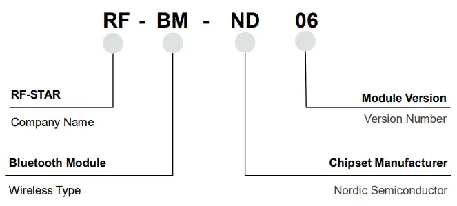
Part Number Conventions
The part numbers are of the form of RF-BM-ND06 where the fields are defined as follows:
FCC Statement
FCC standards: FCC CFR Title 47 Part 15 Subpart C Section 15.247
Integral antenna with antenna gain 0dBi
This device complies with part 15 of the FCC Rules. Operation is subject to the following two conditions:
- This device may not cause harmful interference, and
- this device must accept any interference received, including interference that may cause undesired operation.
Any Changes or modifications not expressly approved by the party responsible for compliance could void the user’s authority to operate the equipment.
Note: This equipment has been tested and found to comply with the limits for a Class B digital device, pursuant to part 15 of the FCC Rules. These limits are designed to provide reasonable protection against harmful interference in a residential installation. This equipment generates, uses and can radiate radio frequency energy and, if not installed and used in accordance with the instructions, may cause harmful interference to radio communications. However, there is no guarantee that interference will not occur in a particular installation. If this equipment does cause harmful interference to radio or television reception, which can be determined by turning the equipment off and on, the user is encouraged to try to correct the interference by one or more of the following measures:
- Reorient or relocate the receiving antenna.
- Increase the separation between the equipment and receiver.
- Connect the equipment into an outlet on a circuit different from that to which the receiver is connected. —Consult the dealer or an experienced radio/TV technician for help.
FCC Radiation Exposure Statement
This modular complies with FCC RF radiation exposure limits set forth for an uncontrolled environment. This transmitter must not be co-located or operating in conjunction with any other antenna or transmitter. If the FCC identification number is not visible when the module is installed inside another device, then the outside of the device into which the module is installed must also display a label referring to the enclosed module. This exterior label can use wording such as the following: “Contains Transmitter Module FCC ID: 2ABN2-RF-BM-ND06 Or Contains FCC ID: 2ABN2-RF-BM-ND06”
When the module is installed inside another device, the user manual of the host must contain below warning statements;
This device complies with Part 15 of the FCC Rules. Operation is subject to the following two conditions:
- This device may not cause harmful interference.
- This device must accept any interference received, including interference that may cause undesired operation.
Note: This equipment has been tested and found to comply with the limits for a Class B digital device, pursuant to part 15 of the FCC Rules. These limits are designed to provide reasonable protection against harmful interference in a residential installation. This equipment generates, uses and can radiate radio frequency energy and, if not installed and used in accordance with the instructions, may cause harmful interference to radio communications.
However, there is no guarantee that interference will not occur in a particular installation. If this equipment does cause harmful interference to radio or television reception, which can be determined by turning the equipment off and on, the user is encouraged to try to correct the interference by one or more of the following measures:
- Reorient or relocate the receiving antenna.
- Increase the separation between the equipment and receiver.
- Connect the equipment into an outlet on a circuit different from that to which the receiver is connected.—Consult the dealer or an experienced radio/TV technician for help.
Changes or modifications not expressly approved by the party responsible for compliance could void the user’s authority to operate the equipment. The devices must be installed and used in strict accordance with the manufacturer’s instructions as described in the user documentation that comes with the product. Any company of the host device which install this modular with modular approval should perform the test of radiated & conducted emission and spurious emission,etc. according to FCC part 15C : 15.247 and 15.209 & 15.207 ,15B Class B requirement, Only if the test result comply with FCC part 15C : 15.247 and 15.209 & 15.207 ,15B Class B requirement, then the host can be sold legally.
Module Configuration and Functions
Module Parameters
Table 1. Parameters of RF-BM-ND06
| Chipset | nRF52840QIAA-R |
| Supply Power Voltage | 1.8 V ~ 5.5 V, recommended to 3.3 V |
| Frequency | 2402 MHz ~ 2480 MHz |
| Maximum Transmit Power | -20.0 dBm ~ +8.0 dBm |
| Receiving Sensitivity | -96 dBm |
| GPIO | 48 |
| Crystal | 32 MHz, 32.768 kHz |
| RAM | 256 KB |
| Flash | 1 MB |
| Package | LGAPackaging |
| Frequency Error | ±20 kHz |
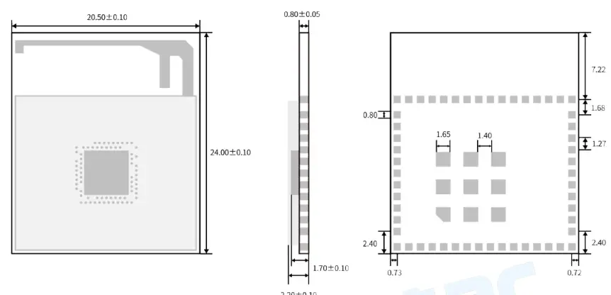
| Dimension | 24.0 mm x 20.5 mm x (2.20 ± 0.1) mm |
| Type of Antenna | PCB Antenna |
| Operating Temperature | -20 ℃~ +70℃ |
| Storage Temperature | -40 ℃~ +125 ℃ |
Module Pin Diagram
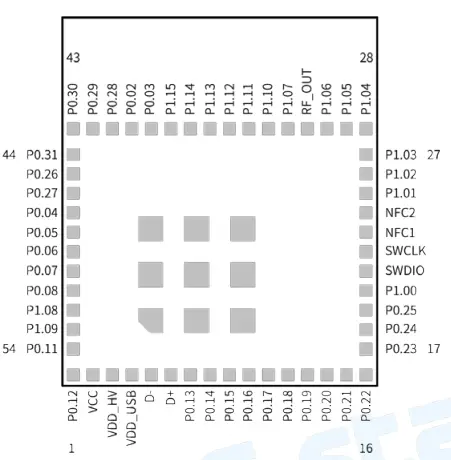
Pin Functions
Table 2. Pin Functions of RF-BM-ND06
| Pin | Name | Chip Pin | Pin Type | Description |
| 1 | P0.12 | SIO_12 | – | – |
| 2 | VCC | Power 1.7V ~ 3.6V | – | 1.7V ~ 3.6V |
| 3 | VDD_HV | Power 2.5V ~ 5.5V | – | 2.5V ~ 5.5V |
| 4 | VDD_USB | 4.35V ~ 5.5V | – | 4.35V ~ 5.5V |
| 5 | D- | D- | Data- | USB- |
| 6 | D+ | D+ | Data+ | USB+ |
| 7 | P0.13 | GPIO_13 | – | LED |
| 8 | P0.14 | GPIO_14 | – | LED |
| 9 | P0.15 | GPIO_15 | – | LED |
| 10 | P0.16 | GPIO_16 | – | LED |
| 11 | P0.17 | GPIO_17 | QSPI_CS | LED |
| 12 | P0.18 | nRESET | – | System reset (active low) |
| 13 | P0.19 | GPIO_19 | QSPI_CLK | – |
| 14 | P0.20 | GPIO_20 | QSPI_DIO0 | – |
| 15 | P0.21 | GPIO_21 | QSPI_DIO1 | – |
| 16 | P0.22 | GPIO_22 | QSPI_DIO2 | – |
| 17 | P0.23 | GPIO_23 | QSPI_DIO3 | – |
| 18 | P0.24 | GPIO_24 | – | – |
| 19 | P0.25 | GPIO_25 | – | – |
| 20 | P1.00 | GPIO_1.00 | – | – |
| 21 | SWDIO | SWDIO | – | Connect to j – link |
| 22 | SWCLK | SWCLK | – | Connect toj – link |
| 23 | NFC1 | NFC1/SIO_09 | – | – |
| 24 | NFC2 | NFC2/SIO_10 | – | – |
| 25 | P1.01 | GPIO_1.01 | – | – |
| 26 | P1.02 | GPIO_1.02 | – | – |
| 27 | P1.03 | nAutoRUN | nAutoRUN | FTDI USB_DTR via jumper on J12pin1-2. |
| 28 | P1.04 | GPIO_1.04 | – | – |
| 29 | P1.05 | GPIO_1.05 | – | – |
| 30 | P1.06 | GPIO_1.06 | – | – |
| 31 | RF_OUT | RF-interface | – | – |
| 32 | P1.07 | GPIO_1.07 | – | – |
| 33 | P1.10 | GPIO_1.10 | – | – |
| 34 | P1.11 | GPIO_1.11 | – | – |
| 35 | P1.12 | GPIO_1.12 | SPI_CS | |
| 36 | P1.13 | GPIO_1.13 | – | – |
| 37 | P1.14 | GPIO_1.14 | – | – |
| 38 | P1.15 | GPIO_1.15 | – | – |
| 39 | P0.03 | GPIO_0.03 | – | Temperature sensor analog |
| 40 | P0.02 | GPIO_0.02 | – | Internal pull low. External pull high to enter into VSP services. |
| 41 | P0.28 | GPIO_0.28 | – | – |
| 42 | P0.29 | GPIO_0.29 | – | – |
| 43 | P0.30 | GPIO_0.30 | – | – |
| 44 | P0.31 | GPIO_0.31 | – | – |
| 45 | P0.26 | GPIO_0.26 | I2C_SDA | I2C RTC chip. I2C data line |
| 46 | P0.27 | GPIO_0.27 | I2C_SCL | I2C RTC chip. I2C clock line. |
|
47 |
P0.04 |
GPIO_0.04 |
SPI_MISO | SPI EEPROM.
SPI_Eeprom_MISO, Input. SPIOPEN in smartBASIC selects SPI function; MOSI and CLK are outputs when in SPI master mode |
| 48 | P0.05 | GPIO_0.05 | UART_RTS | |
| 49 | P0.06 | GPIO_0.06 | UART_TX | |
| 50 | P0.07 | GPIO_0.07 | UART_CTS | |
| 51 | P0.08 | GPIO_0.08 | UART_RX | |
| 52 | P1.08 | GPIO_1.08 | SPI_MOSI | |
| 53 | P1.09 | GPIO_1.09 | SPI_CLK |
Specifications
Recommended Operating Conditions
Functional operation does not guarantee performance beyond the limits of the conditional parameter values in the table below. Long-term work beyond this limit will affect the reliability of the module more or less.
Table 3. Recommended Operating Conditions of RF-BM-ND06
| Items | Condition | Min. | Typ. | Max. | Unit |
| Operating Supply Voltage | Battery Mode | 1.8 | 3.3 | 5.5 | V |
| Operating Temperature | / | -20 | +25 | +70 | ℃ |
| Environmental Hot Pendulum | / | -20 | +20 | ℃/min |
Notes:
- The operating temperature is limited to the operating temperature range of crystal. The temperature range can be wider by changing the crystal.
- To ensure the RF performance, the ripple wave on the source must be less than ±200 mV.
Handling Ratings
Table 4. Handling Ratings of RF-BM-ND06
| Items | Condition | Min. | Typ. | Max. | Unit |
| Storage Temperature | Tstg | -40 | +25 | +85 | ℃ |
| Human Body Model | HBM | ±2000 | V | ||
| Moisture Sensitivity Level | 2 | ||||
| Charged Device Model | ±750 | V |
Notes:
- The storage temperature is limited to the storage temperature range of crystal. The temperature range can be widerby changing the crystal.
Current Consumption
The current consumption characteristics of this module are categorized into different running modes. The overall product level current consumption is averaged over time on different power modes the device runs on. The peripheral circuitry’s current consumption also adds in.
Table 5. Current Consumption of RF-BM-ND06
| Symbol | Description | Min. | Typ. | Max. | Unit |
| Current Consumption: Sleep | |||||
| ION_RAMOFF_EVENT | System ON, no RAM retention, wake on any event | 0.97 | μA | ||
| ION_RAMON_EVENT | System ON, full 256 kB RAM retention, wake on any event | 2.35 | μA | ||
| ION_RAMON_POF | System ON, full 256 kB RAM retention, wake on any event, power-fail comparator enabled | 2.35 | μA | ||
| ION_RAMON_GPIOTE | System ON, full 256 kB RAM retention, wake on GPIOTE input (event mode) | 17.37 | μA | ||
| ION_RAMON_GPIOTEPORT | System ON, full 256 kB RAM retention, wake on GPIOTE PORT event | 2.36 | μA | ||
| ION_RAMOFF_RTC | System ON, no RAM retention, wake on RTC (running from LFRC clock) | 1.50 | μA | ||
| ION_RAMON_RTC | System ON, full 256 kB RAM retention, wake on RTC | 3.16 | μA | ||
| (running from LFRC clock) | |||||
| IOFF_RAMOFF_RESET | System OFF, no RAM retention, wake on reset | 0.40 | μA | ||
| IOFF_RAMOFF_LPCOMP | System OFF, no RAM retention, wake on LPCOMP | 0.86 | μA | ||
| IOFF_RAMON_RESET | System OFF, full 256 kB RAM retention, wake on reset | 1.86 | μA | ||
| ION_RAMOFF_EVENT_5V | System ON, no RAM retention, wake on any event, 5 V supply on VDDH, REG0 output = 3.3 V | 1.29 | μA | ||
| IOFF_RAMOFF_RESET_5V | System OFF, no RAM retention, wake on reset, 5 V supply on VDDH, REG0 output = 3.3 V | 0.95 | μA | ||
| Current Consumption: COMP Active | |||||
| ICOMP,LP | COMP enabled, low power mode | 30.1 | μA | ||
| ICOMP,NORM | COMP enabled, normal mode | 31.8 | μA | ||
| ICOMP,HS | COMP enabled, high-speed mode | 35.1 | μA | ||
| Current Consumption: CPU running | |||||
| ICPU0 | CPU running CoreMark @64 MHz from Flash, Clock = HFXO, Regulator = DC/DC | 3.3 | mA | ||
| ICPU1 | CPU running CoreMark @64 MHz from Flash, Clock = HFXO | 6.3 | mA | ||
| ICPU2 | CPU running CoreMark @64 MHz from RAM, Radio Rx, Clock = HFXO, Regulator = DC/DC | 2.8 | mA | ||
| ICPU3 | CPU running CoreMark @64 MHz from RAM, Radio Rx, Clock = HFXO | 5.2 | mA | ||
| ICPU4 | CPU running CoreMark @64 MHz from flash, Clock = HFINT, Regulator = DC/DC | 3.1 | mA | ||
| Current Consumption: NFCT Active | |||||
| Isense | Current in sense state | 100 | nA | ||
| Iactivated | Current in activated state | 400 | μA | ||
| Current Consumption: Radio Transmitting / Receiving | |||||
| IRADIO_TX0 | Radio transmitting @ 8 dBm output power, 1 Mbps BLEmode, Clock = HFXO, Regulator = DC/DC | 16.4 | mA | ||
| IRADIO_TX1 | Radio transmitting @ 0 dBm output power, 1 Mbps BLE mode, Clock = HFXO, Regulator = DC/DC | 6.4 | mA | ||
| IRADIO_TX2 | Radio transmitting @ -40 dBm output power, 1 Mbps BLE | 3.83 | mA | ||
| mode, Clock = HFXO, Regulator = DC/DC | |||||
| IRADIO_TX3 | Radio transmitting @ 0 dBm output power, 1 Mbps BLE mode, Clock = HFXO | 10.80 | mA | ||
| IRADIO_TX4 | Radio transmitting @ -40 dBm output power, 1 Mbps BLE mode, Clock = HFXO | 4.82 | mA | ||
| IRADIO_TX5 | Radio transmitting @ 0 dBm output power, 250 kbit/s IEE 802.15.4-2006 mode, Clock = HFXO, Regulator = DC/DC | 6.40 | mA | ||
| IRADIO_RX0 | Radio receiving @ 1 Mbps BLE mode, Clock = HFXO, Regulator = DC/DC | 6.26 | mA | ||
| IRADIO_RX1 | Radio receiving @ 1 Mbps BLE mode, Clock = HFXO | 10.10 | mA | ||
| IRADIO_RX2 | Radio receiving @ 250 kbit/s IEE 802.15.4-2006 mode, Clock = HFXO, Regulator = DC/DC | 6.53 | mA | ||
| Current Consumption: RNG Active | |||||
| IRNG0 | RNG running | 635 | μA | ||
| Current Consumption: SAADC Active | |||||
| ISAADC,RUN | SAADC sampling @ 16 ksps, Acquisition time = 20 μs, Clock = HFXO, Regulator = DC/DC | 1.24 | mA | ||
| Current Consumption: TEMP Active | |||||
| ITEMP0 | TEMP started | 1.05 | mA | ||
| Current Consumption: TIMER Running | |||||
| ITIMER0 | One TIMER instance running @ 1 MHz, Clock = HFINT | 418 | μA | ||
| ITIMER1 | Two TIMER instances running @ 1 MHz, Clock = HFINT | 418 | μA | ||
| ITIMER2 | One TIMER instance running @ 1 MHz, Clock = HFXO | 646 | μA | ||
| ITIMER3 | One TIMER instance running @ 16 MHz, Clock = HFINT | 595 | μA | ||
| ITIMER4 | One TIMER instance running @ 16 MHz, Clock = HFXO | 823 | μA | ||
| Current Consumption: WDT Active | |||||
| IWDT,STARTED | WDT started | 3.1 | μA | ||
| Current Consumption: WDT Active | |||||
|
IS0 | CPU running CoreMark from flash, Radio transmitting @ 0 dBm output power, 1 Mbps Bluetooth® low energy (BLE) mode, Clock = HFXO, Regulator = DC/DC |
8.1 |
mA | ||
| IS1 | CPU running CoreMark from flash, Radio receiving @ 1 | 8.6 | mA | ||
| Mbps BLE mode, Clock = HFXO, Regulator = DC/DC | |||||
| IS2 | CPU running CoreMark from flash, Radio transmitting @ 0 dBm output power, 1 Mbps BLE mode, Clock = HFXO | 15.4 | mA | ||
| IS3 | CPU running CoreMark from flash, Radio receiving @ 1 Mbps BLE mode, Clock = HFXO | 16.2 | mA | ||
|
IS4 | CPU running CoreMark from flash, Radio transmitting @ 0 dBm output power, 1 Mbps BLE mode, Clock = HFXO, Regulator = DC/DC, 5 V supply on VDDH, REG0 output = 3.3 V |
11.9 |
mA | ||
|
IS5 | CPU running CoreMark from flash, Radio receiving @ 1 Mbps BLE mode, Clock = HFXO, Regulator = DC/DC, 5 V supply on VDDH, REG0 output = 3.3 V |
12.7 |
mA |
Application, Implementation, and Layout
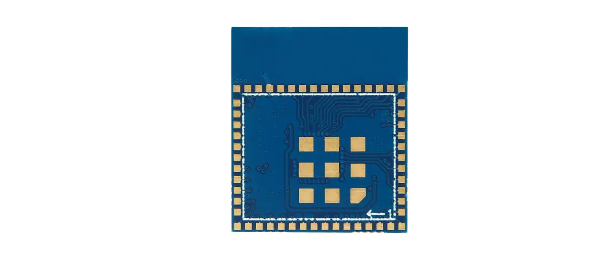
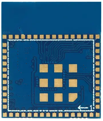
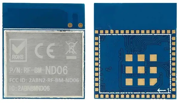
Module Photos
Recommended PCB Footprint
Schematic Diagram
Confidential
Figure 5. Schematic Diagram of RF-BM-ND06
Basic Operation of Hardware Design
- It is recommended to offerthe module with a DC stabilized power supply, a tiny power supply ripple coefficient and the reliable ground. Please pay attention to the correct connection between the positive and negative poles of the power supply. Otherwise, the reverse connection may cause permanent damage to the module;
- Please ensure the supply voltage is between the recommended values. The module will be permanently damaged if the voltage exceeds the maximum value. Please ensure the stable power supply and no frequently fluctuated voltage.
- When designing the power supply circuit for the module, it is recommended to reserve more than 30% of the margin, which is beneficial to the long-term stable operation of the whole machine.The module should be far away from the power electromagnetic, transformer, high-frequency wiring and other parts with large electromagnetic interference.
- The bottom of module should avoid high-frequency digital routing, high-frequency analog routing and power routing.If it has toroute the wire on the bottom of module, for example, it is assumed that the module is soldered to the Top Layer, the copper must be spread on the connection part of the top layer and the module, and be close to the digital part of module and routed in the Bottom Layer (all copper is well grounded).
- Assuming that the module is soldered or placed in the Top Layer, it is also wrong to randomly route the Bottom Layer or other layers, which will affect the spurs and receiving sensitivity of the module to somedegrees;
- Assuming that there are devices with large electromagnetic interference around the module,which will greatly affect themodule performance. It is recommended to stay away from the module according to the strength of the interference. If circumstances permit, appropriate isolation and shielding can be done.
- Assuming that there are routings of large electromagnetic interference around the module (high-frequency digital, high-frequency analog, power routings), which will also greatly affect the module performance. It is recommended to stay away from the module according to the strength of the interference. If circumstances permit, appropriate isolation and shielding can be done.
- It is recommended to stay away from the devices whose TTL protocol is the same2.4 GHzphysical layer, for example: USB3.0.
- The antenna installation structure has a great influence on the module performance. It is necessary to ensure the antenna is exposed and preferably vertically upward. When the module is installed inside of the case, a high-quality antenna extension wire can be used to extend the antenna to the outside of the case.
- The antenna must not be installed inside the metal case, which will cause the transmission distance to be greatly weakened.
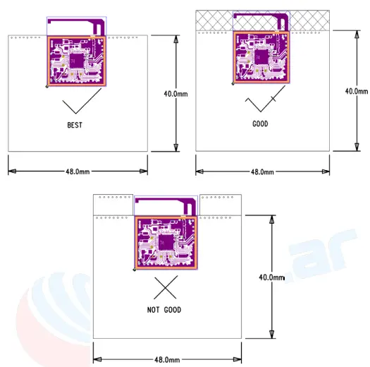
- The recommendation of antenna layout.
The inverted-F antenna position on PCB is free space electromagnetic radiation. The location and layout of antenna is a key factor to increase the data rate and transmission range. Therefore,the layout of the module antenna location and routing is recommended as follows:- Place the antenna on the edge(corner) of the PCB.
- Make sure that there is no signal line or copper foil in each layer below the antenna.
- It is the best to hollow out the antenna position in the following figure so as to ensure that S11 of the module is minimally affected.
Trouble Shooting
Unsatisfactory Transmission Distance
- When there is a linear communication obstacle, the communication distance will be correspondingly weakened.Temperature, humidity, and co-channel interference will lead to an increase in communication packet loss rate.The performances of ground absorption andreflectionof radio waves will be poor, when the module is tested close to the ground.
- Seawater has a strong ability to absorb radio waves, so the test results by seaside are poor.
- The signal attenuation will be very obvious, if there is a metal near the antenna or themodule is placed inside of the metal shell.
- The incorrect power register set or the high data ratein an open air may shorten the communication distance.The higher the data rate, the closer the distance.
- The low voltage of the power supply is lower than the recommended value at ambient temperature, and the lower the voltage, the smaller the power is.
- The unmatchable antennas and module or the poor quality of antenna will affect the communication distance.
Vulnerable Module
- Please ensure the supply voltage is between the recommended values. The module will be permanently damaged if the voltage exceeds the maximum value. Please ensure the stable power supplyand no frequently fluctuatedvoltage.
- Please ensure the anti-static installation and the electrostatic sensitivity of high-frequency devices.
- Due to some humidity sensitive components, please ensure the suitable humidity during installation and application.If there is no special demand, it is not recommended to use at too high or too low temperature.
High Bit Error Rate
- There areco-channel signal interferences nearby.It is recommended to be away from the interference sources or modify the frequency and channel to avoid interferences.
- The unsatisfactory power supply may also cause garbled. It is necessary to ensure the power supply reliability.
- If the extension wire or feeder wire is of poor quality or too long, the bit error rate will be high.
Electrostatics Discharge Warnings
The module will be damaged for the discharge of static. RF-star suggest that all modules should follow the 3 precautions below:
- According to the anti-static measures, bare hands are not allowed to touch modules.
- Modules must be placed in anti- static areas.
- Take the anti-static circuitry (when inputting HV or VHF) into consideration in product design. Static may result in the degradation in performance of module, even causing the failure.
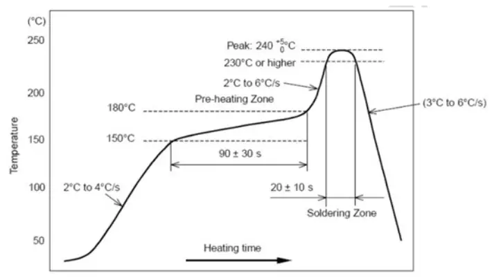
Soldering and Reflow Condition
- Heating method: Conventional Convection or IR/convection.
- Temperature measurement: Thermocouple d = 0.1 mm to 0.2 mm CA (K) or CC (T) at soldering portion or equivalent methods.
- Solder paste composition: Sn/3.0 Ag/0.5 Cu
- Allowable reflow soldering times: 2 times based on the following reflow soldering profile.
- Temperature profile: Reflow soldering shall be done according to the following temperature profile.
- Peak temperature: 245 ℃.
Optional Packaging
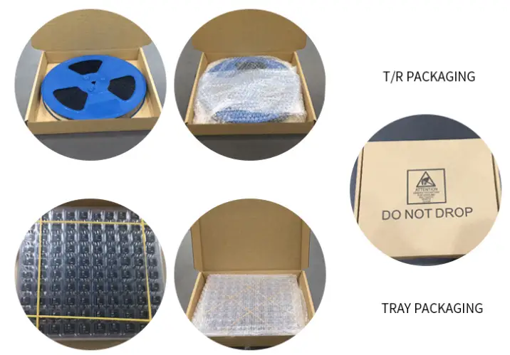
Note: Default tray packaging.
Certification
RoHS
RoHS Report No.: BLA-C-201811-A05-01

Revision History
| Date | Version No. | Description | Author |
| 2018.10.26 | V1.0 | The initial version is released. | Aroo Wang |
| 2018.12.06 | V1.0 | Update module Parameter. | Aroo Wang |
Contact Us
SHENZHEN RF-STAR TECHNOLOGY CO., LTD.
Shenzhen HQ:
Add.: Room 601, Block C, Skyworth Building, High-tech Park, Nanshan District, Shenzhen, Guangdong, China Tel.: 86-755-8632 9687
Chengdu Branch:
Add.: No. B4-12, Building No.1, No. 1480 Tianfu Road North Section (Incubation Park), High-Tech Zone, Chengdu, China (Sichuan) Free Trade Zone, 610000
Tel.: 86-28-6577 5970
Email: [email protected], [email protected]
Web.: www.szrfstar.com


 Module User Manual")


