![]() User Manual
User Manual
AB5303B Bluetooth module
Product Overview
1.1 Introduce
AB53XX is a 32 bits RISC microcontroller. It integrates advanced digital and analog peripherals to audio player applications.
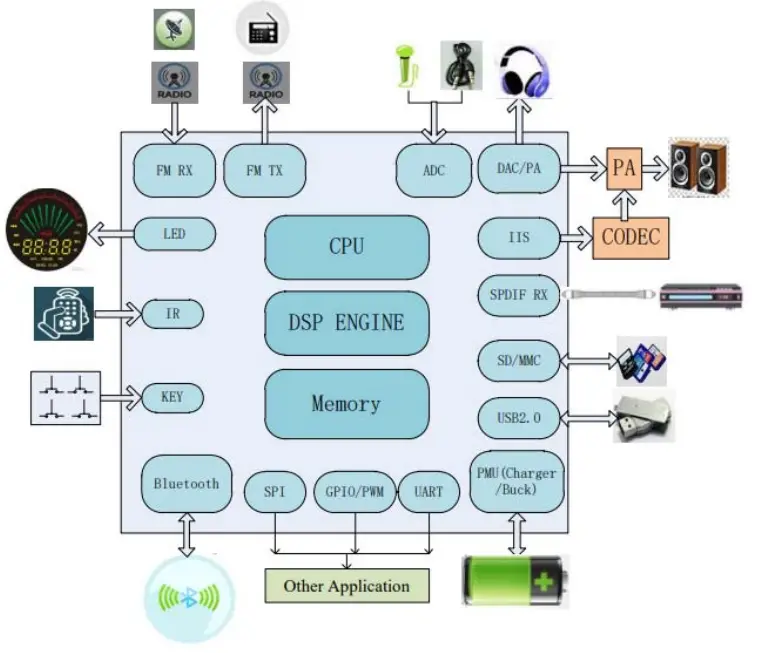
1.2 Features
CPU and Flexible IO
- 32bit High performance CPU with DSP instruction
- Flexible GPIO pins with Programmable pull-up and pull-down resistors;
- Support GPIO wakeup or interrupt;
Bluetooth Radio
- Compliant to Bluetooth and BLE specification
- Max output power:-4.41dbm(BLE);-1.2dbm(BT)
- Operation Frequency:2402-2480MHz
FM Tuner
- Support frequency band 76~108MHz;
- Auto search tuning;
- Programable de-emphasis(50/75uS);
- Receive signal strength indicator (RSSI);
Audio Interface
- Audio codec with 16bit stereo DAC and two channel 16bit ADC;
- Support flexible audio EQ adjust;
- Support Sample rate 8, 11.025, 12, 16, 22.05, 32, 44.1 and 48KHz;
- 4 channel Stereo Analog MUX;
- Two channel MIC amplifier input;
- High performance Stereo audio ADC with 90dB SNR
- High performance Stereo audio DAC with 95dB SNR, with headphone amplifier output;
Peripheral and Interfaces
- Three 32-bit timers;
- Three multi-function 32-bit timers, support Capture and PWM mode;
- WatchDog;
- Three full-duplex UART;
- SPI;
- IR controller;
- SD Card Host controller;
- Full speed USB 2.0 HOST/DEVICE controller;
- Sixteen Channels 10-bit SARADC;
- Build in PMU, such as LDO;
Temperature
- Operating temperature: -40℃ to +85℃;
- Storage temperature: -65℃ to +150℃;
Package Definition
2.1 Pin Assignment
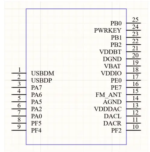
Pin No. | Name | Type | Function |
| 1 | USBDM | I/O | ADC6/USB/DM/SPI0CLK-G3/RX0-G3/PB4 |
| 2 | USBDP | I/O | ADC5/USB/DP/SPI0DO-G3/TX0-G3/PB3 |
| 3 | PA7 | I/O | ADC2/AUXR0/SDDAT0-G1/SPI1DO-G2/TX0-G1/T X1-G1/HSTRX-G1/PWM2-T4/PA7 |
| 4 | PA6 | I/O | ADC1/AUXL0/SDCLK-G1/SPI1CLK-G2/RX0-G1/R X1-G1/HSTRX-G6/FMOSC-2/PWM1-T4/TMR3CAP_G2/ IR_G2/PA6 |
| 5 | PA5 | I/O | ADC0/SDCMD-G1/SPI1DI-G2/FMOSC-G1/PWM0 -T4/TMR3CAP_G1/IR_G1/PA5 |
| 6 | PA2 | I/O | SPI1DI-G1/LPWM2-G3/IISSCLK-G1/PA2 |
| 7 | PA0 | I/O | SPDIF0/RX0-G5/HSTRX-G10/LPWM0-G3/IISDI-G1/PA0 |
| 8 | PF5 | I/O | PF5 |
| 9 | PF4 | I/O | PF4 |
| 10 | MICL/PF2 | I/O | ADC10/MICL/SPI1DO-G5/TX0-G7/LPWM3-G2/PF 2 |
| 11 | DACR | A | DAC R |
| 12 | DACL | A | DAC L |
| 13 | VDDDAC | PWR | DAC powe |
| 14 | AGND | GND | DAC Ground |
| 15 | FM_ANT | A | FMRX ANT |
| 16 | PE7 | I/O | ADC9/AUXR2/SDDAT0-G3/SPI1DO-G4/TX0-G4/ HSTRX-G4/LPWM3-G1/TMR4CAP_G1/IR_G8/PE7 |
| 17 | PE0 | I/O | SPI0DI-G3/TX0-G6/LPWM2-G2/IISDI-G2/TMR3C AP_G5/IR_G5/PE0 |
| 18 | VDDIO | PWR | VDDIO power output |
| 19 | VBAT | PWR | VBAT power input |
| 20 | DGND | GND | Digital Ground |
| 21 | VDDBT | PWR | BT power |
| 22 | PB2 | I/O | ADC4/AUXR1/SDDAT0-G2/SPI1DO-G3/TX0-G2/T X2-G2/HSTRX-G2/PWM2-T3/PB2 |
| 23 | PB1 | I/O | ADC3/FM/AM-G1/AUXL1/SDCLK-G2/SPI1CLK-G 3/RX0-G2/RX2-G2/HSTRX-G7/FMOSC-G4 |
| 24 | PWRKEY | A | Power key input |
| 25 | PB0 | I/O | FM/AM-G0/SPDIF2/SDCMD-G2/SPI1DI-G3/FMO SC-G3/PWM0- /TMR3CAP_G3/IR_G3/PB0 |
Characteristics
3.1 PMU Parameters
Table 3-1 PMU voltage input Parameters
| Sym | Characteristics | Min | Typ | Max | Unit |
| VUSB | Charger Voltage input | 3.0 | 5.0 | 5.0 | V |
| VBAT | Voltage input | 3.0 | 3.7 | 5.0 | V |
Table 3-2 3.3V LDO Parameters
| Sym | Characteristics | Min | Typ | Max | Unit |
| VDDIO @ Light Loading | 3.3V LDO voltage output | 3.0 | 3.3 | 3.6 | V |
| △VVDDIO @ VDDIO=3.3v | Output Mismatch 1-sigma | – | 56 | – | mV |
| ILOAD @@VBAT=3.6v | Maximum output current | – | – | 150 | mA |
| ISC @VBAT=3.8v | Short Circuit Current Limit | – | – | 300 | mA |
Table 3-3 1.6V LDO Parameters
| Sym | Characteristics | Min | Typ | Max | Unit |
| VDDBT @ Light Loadingcondition | 1.6V LDO voltage output | – | 1.6 | – | V |
| △VVDDBT@ VDDBT=1.6v | Output Mismatch 1-sigma | – | 27 | – | mV |
| ILOAD@VBAT=3.0v | Maximum output current | – | – | 100 | mA |
| ISC | Short Circuit Current Limit | – | – | 200 | mA |
| @VBAT=3.8v |
Table 3-4 1.2V LDO Parameters
| Sym | Characteristics | Min | Typ | Max | Unit |
| VDDCORE @ Light Loading condition | 1.2V LDO voltage output | – | 1.2 | – | V |
| △VVDDCORE @ VDDCORE=1.2v | Output Mismatch 1-sigma | – | 20 | – | mV |
| ILOAD @VBAT=3.6v | Maximum output current | – | – | 80 | mA |
| ISC @VBAT=3.8v | Short Circuit Current Limit | – | – | 120 | mA |
3.2 IO Parameters
Table 3-5 I/O Parameters
Symbol | Description | Min | Typ | Max | Unit |
| VIL@VDDIO=3.3V | Low-level input voltage | -0.3 | 1.27 | V | |
| VIH @VDDIO=3.3V | High-level input voltage | 2.03 | 3.6 | V | |
| Driver Ability 1 @VDDIO=3.3V | Output Driver Ability 1 | 32 | mA | ||
| Driver Ability 0 @VDDIO=3.3V | Output Driver Ability 0 | 8 | mA | ||
| RPUP0 | Internal pull-up resister 0 | 8 | 10 | 12 | KΩ |
| RPUP1 | Internal pull-up resister 1 | 0.24 | 0.3 | 0.36 | KΩ |
| RPUP2 | Internal pull-up resister 2 | 160 | 200 | 240 | KΩ |
| RPDN0 | Internal pull-down resister 0 | 8 | 10 | 12 | KΩ |
| RPDN1 | Internal pull-down resister 1 | 0.24 | 0.3 | 0.36 | KΩ |
| RPDN2 | Internal pull-down resister 2 | 160 | 200 | 240 | KΩ |
3.3 Audio DAC Parameters
Table 3-6 Audio DAC Parameters
Sym | Characteristics | Min | Typ | Max | Unit | Conditions |
| SNR | – | 96 | – | dB | VCM cap=1uF VDDDAC cap=1uF with A-wt filter Output -3dBv Fin=1KHz | |
| THD+N | – | -86 | – | dB | VCM cap=1uF VDDDAC cap=1uF with A-wt filter Output -3dBv with 10k loading Fin=1KHz | |
| Output Range | Maximum output voltage | – | 2.6 | VPP | 32ohm Loading |
3.4 Audio ADC Parameters
Table 3-7 Audio ADC Parameters
| Sym | Characteristics | Min | Typ | Max | Unit | Conditions |
| SNR | – | 90 | – | dB | VCM cap=1uF VDDDACcap=1uF with A-wt filter Input sine amplitude, 850mV RMS Fin=1KHz | |
| THD+N | – | -87 | – | dB | VCM cap=1uF VDDDACcap=1uF with A-wt filter Input sine amplitude, 850mV RMS Fin=1KHz. | |
| Input Range | Input sine wave peak amplitude | 0 | VCM | V | From aux input, 0db gain, representVCM voltage. |
3.5 BT Parameters
Table 3-8 BT Parameters
| Characteristics | Min | Typical | Max | Unit | Conditions |
| RMSDEVM | – | 5.5 | – | % | Maximum TX power 2-DH5 packet |
| Peak DEVM | – | 12.5 | % | ||
| EDR Relative Transmit Power | -0.2 | – | dB | ||
| Sensitivity @ Basic Rate | -90.5 | dBm | BER=0.1%, using DH5 packet | ||
| Sensitivity @ EDR | -89.5 | dBm | BER=0.01%, using 2-DH5 packet |
3.6 Current Parameters
Table 3-9 Current Parameters
| Sym | Characteristics | Min | Typ | Max | Unit | Conditions |
| IRTC | RTC mode current | – | 4 | – | uA | 4.2Vinput, room temp. |
| Sleep | Sleep current | – | 500 | 2000 | uA | 3.3V input, room temp |
Hardware Description
4.1 Module size and Pin assignment
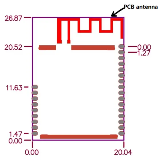
4.2 PCB Layout Guide
Bluetooth works in a frequency of 2.4GHz, the design of PCB and
Mechanical should be careful to avoid the impact of various factors on the RF performance. Please note the following:
- Outer casing surrounding AB5303B module should avoid using metal materials. If the casing is metal, it is recommended to use an external 2.4GHz antenna.
- Metal screws should be far away from RF part of module.
- Module should be placed on the edge of motherboard, ensure the antenna towards outside. Please make sure that all layers have no trace or copper under the Antenna region.
Caution
Any Changes or modifications not expressly approved by the party responsible for compliance could void the user’s authority to operate the equipment.
This device complies with part 15 of the FCC Rules. Operation is subject to the following two conditions:
- This device may not cause harmful interference, and
- This device must accept any interference received, including interference that may cause undesired operation.
Note: This equipment has been tested and found to comply with the limits for a Class B digital device, pursuant to part 15 of the FCC Rules. These limits are designed to provide reasonable protection against harmful interference in a residential installation. This equipment generates, uses and can radiate radio frequency energy and, if not installed and used in accordance with the instructions, may cause harmful interference to radio communications. However, there is no guarantee that interference will not occur in a particular installation. If this equipment does cause harmful interference to radio or television reception, which can be determined by turning the equipment off and on, the user is encouraged to try to correct the interference by one or more of the following measures:
—Reorient or relocate the receiving antenna.
—Increase the separation between the equipment and receiver.
—Connect the equipment into an outlet on a circuit different from that to which the receiver is connected.
—Consult the dealer or an experienced radio/TV technician for help.
OEM Guidance
- Applicable FCC rules
This device complies with part 15.247 of the FCC Rules. - The specific operational use conditions
This module can be used in IoT devices. The input voltage to the module is nominally 3.3 V DC. The operational ambient temperature of the module is -40 °C ~ 85 °C. the external antenna is allowed, such as PCB antenna. - Limited module procedures N/A
- Trace antenna design N/A
- RF exposure considerations The equipment complies with FCC radiation exposure limits set forth for an uncontrolled environment.
- Antenna Antenna type: PCB antenna; Peak antenna gain : 5.3 dBi
- Label and compliance information An exterior label on OEM’s end product can use wording such as the following: “Contains Transmitter Module FCC ID: OCDAB5303B” or “Contains FCC ID: OCDAB5303B”
- Information on test modes and additional testing requirements a.
The modular transmitter has been fully tested by the module grantee on the required number of channels, modulation types, and modes, it should not be necessary for the host installer to re-test all the available transmitter modes or settings. It is recommended that the host product manufacturer, installing the modular transmitter,perform some investigative measurements to confirm that the resulting composite system does not exceed the spurious emissions limits or band edge limits (e.g., where a different antenna may be causing additional emissions).
b. The testing should check for emissions that may occur due to the intermixing of emissions with the other transmitters, digital circuitry, or due to physical properties of the host product (enclosure). This investigation is especially important when integrating ultiple modular transmitters where the certification is based on testing each of them in a standalone configuration. It is important to note that host product manufacturers should not assume that because the modular transmitter is certified that they do not have any responsibility for final product compliance.
c. If the investigation indicates a compliance concern the host product manufacturer is obligated to mitigate the issue. Host products using a modular transmitter are subject to all the applicable individual technical rules as well as to the general conditions of operation in Sections 15.5, 15.15, and 15.29 to not cause interference. The operator of the host product will be obligated to stop operating the device until the interference have been corrected . - Additional testing, Part 15 Sub part B disclaimer The final host / module combination need to be evaluated against the FCC Part 15B criteria for unintentional radiators in order to be properly authorized for operation as a Part 15 digital device.
The host integrator installing this module into their product must ensure that the final composite product complies with the FCC requirements by a technical assessment or evaluation to the FCC rules, including the transmitter operation and should refer to guidance in KDB 996369. For host products with certified modular transmitter, the frequency range of investigation of the composite system is specified by rule in Sections 15.33(a)(1) through (a)(3), or the range applicable to the digital device, as shown in Section 15.33(b)(1), whichever is the higher frequency range of investigation When testing the host product, all the transmitters must be operating. The transmitters can be enabled by using publicly-available drivers and turned on, so the transmitters are active. In certain conditions it might be appropriate to use a technology-specific call box (test set) where accessory 50 devices or drivers are not available. When testing for emissions from the unintentional radiator, the transmitter shall be placed in the receive mode or idle mode, if possible. If receive mode only is not possible then, the radio shall be passive (preferred) and/or active scanning. In these cases, this would need to enable activity on the communication BUS (i.e., PCIe, SDIO, USB) to ensure the unintentional radiator circuitry is enabled. Testing laboratories may need to add attenuation or filters depending on the signal strength of any active beacons (if applicable) from the enabled radio(s). See ANSI C63.4,
ANSI C63.10 and ANSI C63.26 for further general testing details.
The product under test is set into a link/association with a partnering device, as per the normal intended use of the product. To ease testing, the product under test is set to transmit at a high duty cycle, such as by sending a file or streaming some media content.
![]()


