![]()
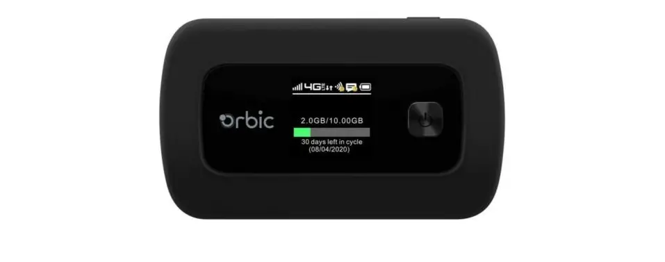
Reliance Communications RC101ML Orbic 4G Module
Overview
Orbic 4G Module is a 4G universal module, can be used for MIFI, notebook and other products. It integrates the low power Qualcomm SDX12 application processor that is designed for the 4G Module.. The SDX12 uses the 14 nm process for lower active power dissipation and faster peak CPU performance. It includes a 1.28 GHz Cortex-A7 application processor and a 1 GHz Qualcomm® Hexagon™ DSP 6 modem processor.
Parameter
| Type | Items | Performance |
|
Hardware | Working Voltage | 3.6-4.2V |
| Working Current | 200 ~ 650mA | |
| Standby Current | 8mA | |
| Operating Ambient Temperature | -10℃ ~ 60℃ | |
| Storage Temperature | -20℃ ~80℃ |
Hardware Description
Description of Hardware Interface
Orbic 4G Module provides 4 RF connectors for external antenna connection.As shown in Figure 2-1, “1” is the RF main antenna, which is used for receiving and receiving RF signals.”4″ is the Diversity antenna for receiving the Diversity radio signals. “2” is the B48 main antenna, which is used for receiving and receiving B48 RF signals.”3″ is the B48 Diversity antenna for receiving the Diversity radio signals.
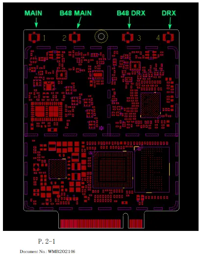
| BAND | MAIN | DRX | B48 MAIN | B48 DRX |
| LTE TRX: B2/4/5/7/12/13/14/17/25/26/29/41/66/71 WCDMA TRX: B2/4/5 |
√ | |||
| LTE DRX: LTE: B2/4/5/7/12/13/14/17/25/26/29/41/66/71 WCDMA DRX: B2/4/5 |
√ | |||
|
B48 TRX: B48 |
√ | |||
|
B48 DRX: B48 |
√ |
Pin Description.
The following figures is the PIN identification of the module:
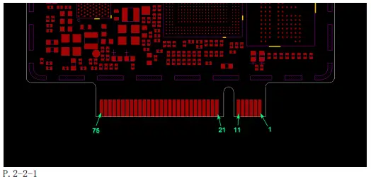
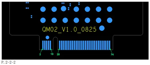
Pin Description:
| PIN# | PIN name | I/O | Reset Value | PIN description | characterist |
| 1 | CONFIG_3 | O | NC | NC,Module internal configuration。 | 1.8V |
| 2 | VCC | PI | – | Power input | Power |
| 3 | GND | – | – | GND | Power |
| 4 | VCC | PI | – | Power input | Power |
| 5 | GND | – | – | GND | Power |
| 6 | NC | – | – | – | |
| 7 | USB D+ | I/O | – | USB 2.0 data + | 0.3-3V |
| 8 | GPIO_85 | I | PU | reserve | |
| 9 | USB D- | I/O | – | USB2.0 data – | 0.3-3V |
| 10 | GPIO_4 | O | T | NA | CMOS 1.8V |
| 11 | GND | – | – | GND | Power |
| 12 | Notch | – | – | Notch | – |
| 13 | Notch | – | – | Notch | – |
| 14 | Notch | – | – | Notch | – |
| 15 | Notch | – | – | Notch | – |
| 16 | Notch | – | – | Notch | – |
| 17 | Notch | – | – | Notch | – |
| 18 | Notch | – | – | Notch | – |
| 19 | Notch | – | – | Notch | – |
| 20 | GPIO_6 | O | PU | reserve | |
| 21 | CONFIG_0 | – | NC | NC | – |
| 22 | GPIO_7 | I | PU | reserve | |
| 23 | M2_WOWWAN_ | O | PD | NA | CMOS 1.8V |
| 24 | GPIO_18 | O | PU | reserve |
| PIN# | PIN name | I/O | Reset Value | PIN description | characterist |
| 25 | M2_DPR | I | PU | reserve | CMOS 1.8V |
| 26 | M2_W_DISABLE 2# | I | PU | reserve | CMOS 1.8V |
| 27 | GND | – | – | GND | Power |
| 28 | GPIO_68 | O | PU | reserve | |
| 29 | USB_SS -TX- | O | – | USB3.0 reserve | – |
| 30 | UIM1_RESET | O | L | SIM 1 | CMOS 1.8V |
| 31 | USB_SS -TX+ | O | – | USB3.0 reserve | – |
| 32 | UIM1_CLK | O | L | SIM 1 | CMOS 1.8V |
| 33 | GND | – | – | GND | Power |
| 34 | UIM1_DATA | I/O | L | SIM 1 | CMOS 1.8V |
| 35 | USB_SS-RX – | I | – | USB3.0 reserve | – |
| 36 | UIM1_PWR | PO | – | SIM 1 | CMOS 1.8V |
| 37 | USB_SS-RX+ | I | USB3.0 reserve | – | |
| 38 | NC | – | – | – | – |
| 39 | GND | – | – | GND | Power |
| 40 | SIM2_DETECT | I | PU | SIM 2 | CMOS 1.8V |
| 41 | PCIE_TX0_M | O | – | PCIe | – |
| 42 | UIM2_DATA | I/O | L | SIM 2 | CMOS 1.8V |
| 43 | PCIE_TX0_P | O | – | PCIe | – |
| 44 | UIM2_CLK | O | L | SIM 2 | CMOS 1.8V |
| 45 | GND | – | – | GND | Power |
| 46 | UIM2_RESET | O | L | SIM 2 | CMOS 1.8V |
| 47 | PCIE_RX0_M | I | – | PCIe | – |
| PIN# | PIN name | I/O | Reset Value | PIN description | characteristi |
| 48 | UIM2_PWR | PO | – | SIM 2 | CMOS 1.8V |
| 49 | PCIE_RX0_P | I | – | PCIe | – |
| 50 | PCIE_RST_N | I | PD | PCIe | CMOS 1.8V |
| 51 | GND | – | – | GND | Power |
| 52 | PCIE_CLKREQ_N | I/O | T | PCIe | CMOS 1.8V |
| 53 | PCIE_REFCLK_M | I | – | PCIe | – |
| 54 | PXIE_WAKE_N | O | T | PCIe | CMOS 1.8V |
| 55 | PCIE_REFCLK_P | I | – | PCIe | – |
| 56 | ANTCTL1 | O | PD | Antenna switch | CMOS 1.8V |
| 57 | GND | – | – | GND | Power |
| 58 | ANTCTL2 | I/O | PD | Antenna switch | CMOS 1.8V |
| 59 | GPIO_43 | O | PU | reserve | |
| 60 | WLAN_TX_EN | I | – | WLAN switch | CMOS 1.8V |
| 61 | GPIO_17 | O | PU | reserve | |
| 62 | COEX_UART_RX | I | PD | WiFi/BT UART | CMOS 1.8V |
| 63 | NC | O | – | – | CMOS 1.8V |
| 64 | COEX_UART_TX | O | PD | WiFi/BT UART | CMOS 1.8V |
| 65 | NC | O | – | – | CMOS 1.8V |
| PIN# | PIN name | I/O | Reset Value | PIN description | characteristi |
| 66 | SIM_DETECT | I | PU | SIM 1 | CMOS 1.8V |
| 67 | M2_RESET_N | I | PU | Module reset | CMOS 1.8V |
| 68 | FORCE_USB_BO OT | Download mode switch | CMOS 1.8V | ||
| 69 | CONFIG_1 | O | GND | NC, | – |
| 70 | VCC | PI | – | VCC | Power |
| 71 | GND | – | – | GND | Power |
| 72 | VCC | PI | – | VCC | Power |
| 73 | NC | – | – | – | |
| 74 | VCC | PI | – | VCC | Power |
| 75 | CONFIG_2 | O | NC | NC |
Reset Value:
- H:High level
- L:Low level
- PD:pull down
- PU:pull up
- T: Hi-Z。
- OD:Open drain
- PP:Push-Pull
- PI:Power in
- PO:Power out
Mechanical Dimension
Module has the dimension of 46mm x 36mm. The detailed layout will be given shortly below. Unit: mm
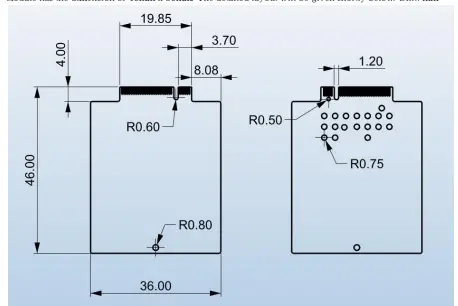
PLUG PCB dimensions:
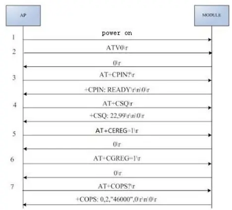
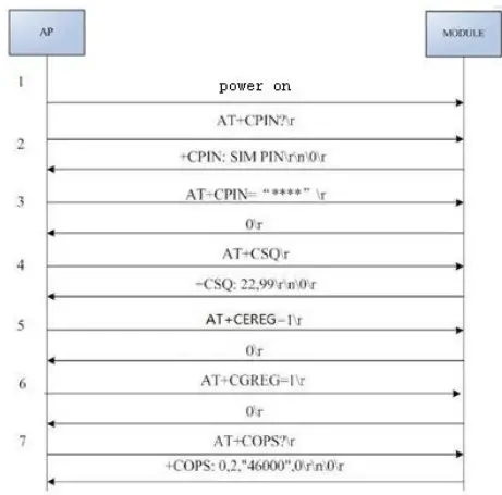
Software Introduction
Normal power on
PIN code needed power on
Module Environmental and Package
Environmental Ratings
The environmental ratings are shown as following table.
| Characteristic | Value | Units | Conditions/Comments |
| Storage Temperature | -20 ~ 80 | ℃ | |
| Relative humidity | Less than 60 | % | Storage |
| Less than 80 | % | Operation |
Electrostatic Discharge Specifications
Extreme caution must be exercised to prevent electrostatic discharge (ESD) damage. Proper use of wrist and heel grounding straps to discharge static electricity is required when handling these devices. Always store unused material in its antistatic packaging.
ESD Specifications
| Type | Symbol | Condition | ESD Rating | Unit |
| ESD Handling | ESD_HAND_HBM | Human Body Model Contact Discharge per JEDEC EID/JESD22-A114 | 1000 | V |
| Machine Model (MM) | ESD_HAND_MM | Machine Model Contact | 30 | V |
| CDM | ESD_HAND_CDM | Charged Device Model Contact Discharge per JEDEC EIA/JESD22-C101 | 300 | V |
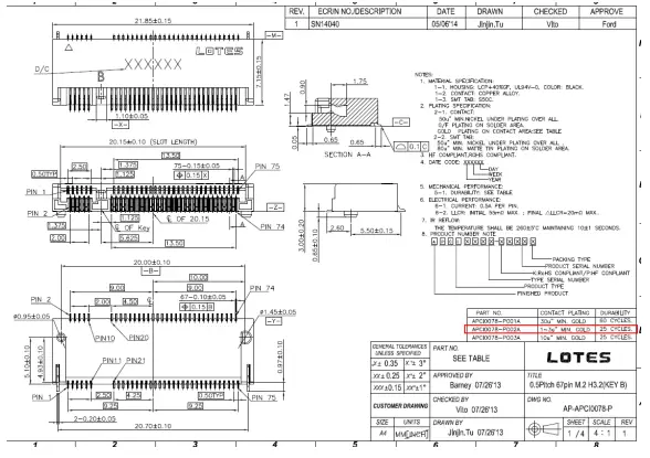
Ordering Information
Table 5-1 Part Ordering Information
FCC Information
RF Exposure Information: To maintain compliance with FCC RF exposure requirements, use the product that maintain a 20cm separation distance between the user’s body and the host.
FCC statements:
This device complies with part 15 of the FCC rules. Operation is subject to the following two conditions:
- this device may not cause harmful interference, and
- this device must accept any interference received, including interference that may cause undesiredoperation.
NOTE: The manufacturer is not responsible for any radio or TV interference caused by unauthorizedmodifications or changes to this equipment. Such modifications or changes could void the user’s authority tooperate the equipment.
NOTE: This equipment has been tested and found to comply with the limits for a Class B digital device, pursuantto part 15 of the FCC Rules. These limits are designed to provide reasonable protection against harmfulinterference in a residential installation. This equipment generates uses and can radiate radio frequency energyand, if not installed and used in accordance with the instructions, may cause harmful interference to radio communications. However, there is no guarantee that interference will not occur in a particular installation. Ifthis equipment does cause harmful interference to radio or television reception, which can be determined byturning the equipment off and on, the user isencouraged to try to correct the interference by one or more of thefollowing measures:
- Reorient or relocate the receiving antenna.
- Increase the separation between the equipment and receiver.
- Connect the equipment into an outlet on a circuit different from that to which the receiver is connected.
- ‐Consult the dealer or an experienced radio/TV technician for help.
This device is intended only for OEM integrators under the following conditions:
1. The antenna must be installed such that 20 cm is maintained between the antenna and users. 2. The transmitter module may not be co-located with any other transmitter or antenna. As long as the two conditions above are met, additional transmitter testing will not be required. However, the OEM integrator is still responsible for testing their end-product for any additional compliance requirements required for the installed module.
Important Note:
In the event that these conditions cannot be met (for example certain laptop configurations or co-location with another transmitter), then the Federal Communications Commission of the U.S. Government (FCC) and the Canadian Government authorizations are no longer considered valid and the FCC ID cannot be used on the final product. In these circumstances, the OEM integrator shall be responsible for re-evaluating the end-product (including the transmitter) and obtaining a separate FCC authorization in the U.S. and Canada.
OEM Integrators – End Product Labeling Considerations:
This transmitter module is authorized only for use in device where the antenna may be installed such that 20 cm may be maintained between the antenna and users. The final end product must be labeled in a visible area with the following: “Contains, FCC ID: 2ABGH-RC101ML”. The grantee’s FCC ID can be used only when all FCC compliance requirements are met.
OEM Integrators – End Product Manual Provided to the End User:
The OEM integrator shall not provide information to the end user regarding how to install or remove this RF module in end product user manual. The end user manual must include all required regulatory information and warnings as outlined in this document.


