![]()
MGA6230A CAT12 Module
User Manual
MGA6230A Module
Product User Manual
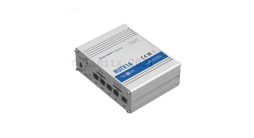
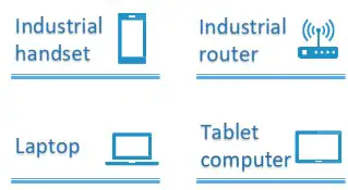
MGA6230Amodule is an industrial-grade LTE module, which provides multiple bands support. This module can be adapted to various types of terminal devices, providing LTE network connection and data communication, such as industrial routers, industrial handsets, tablet computers, laptops, etc.
General Features
| Main Chipset | GCT GDM7243A |
| LTE Category | 3GPP Release11 Cat12 |
| Band support | B2/4/5/12/13/66/71 |
| Antenna | 4 ANT PINLTE: Main and Diversity antenna |
| Tx/Rx | B2/4/66,2T4R B5/12/13/71,1T2R DL: 2CA intra band ,4×4 MIMO |
| CA/MIMO | 2CA inter band ,2×2 MIMO 3CA&4CA,2×2 MIMO |
| Modulation | UL: 2CA 2x2MIMO Uplink: QPSK/16QAM/64QAM Downlink: QPSK/16QAM/64QAM/256QAM |
| Power output | +23dBm (Power Class3) |
| Throughput | DL: Max 600Mbps UL: Max 150Mbps |
| Interface | USB 2.0&USB3.0 UART、SIM*1、PCIE、RGMII GPIO、SDIO、SPI、PCM |
| Voltage Input | 3.0VDC ~ 3.6VDC ( Recommend 3.3V) |
| Operating Temperature | -40℃~+85℃ (Reduce RF performance: -40℃~-30℃, |
| Storage Temperature | +70℃~+85℃) -40℃~+85℃ |
Dimensions
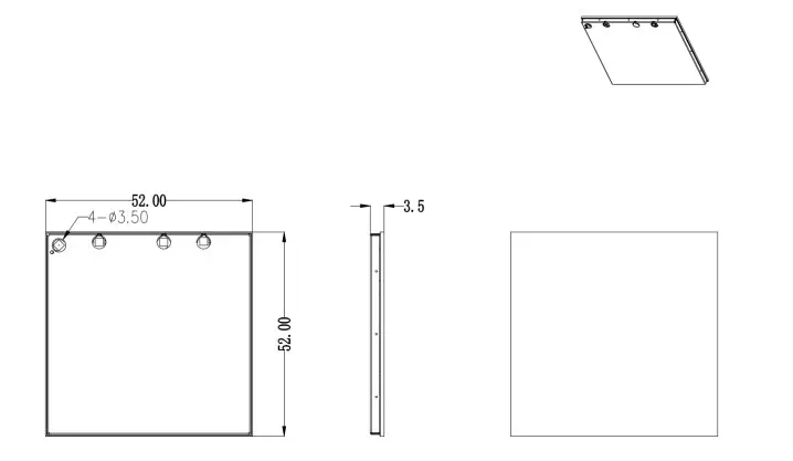
Fig. 1 – Detail module dimension
Pin Definition
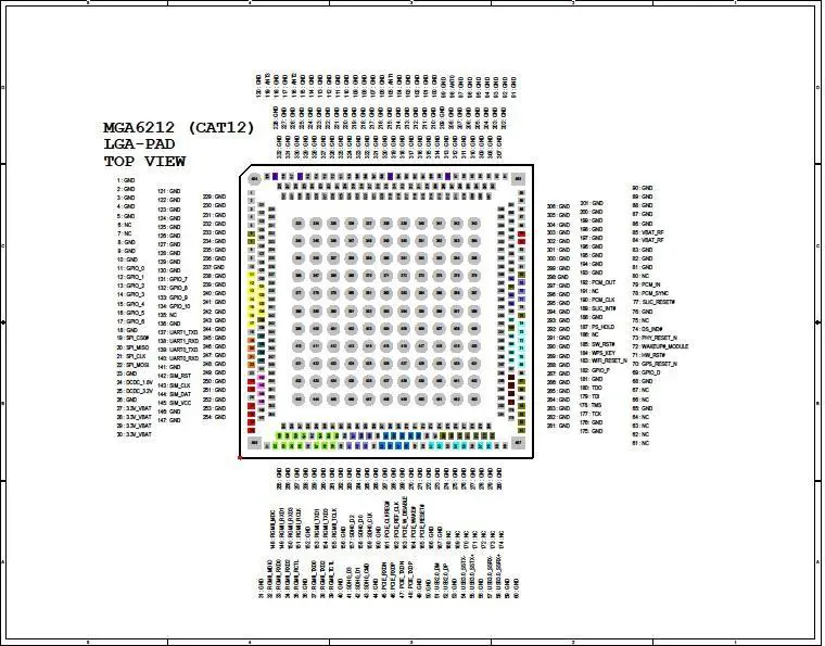
Pin Description
| Pin Name | Pin No. | Description | I/O | Voltage Domain |
| Power | ||||
| 3.3V_VBAT | 27,28,29,30 | Power supply for the module’s baseband part | PI | 3.0V-3.6V |
| VBAT_RF | 84,85 | Power supply for the module’s RF part | PI | 3.3V-4.3V |
| DCDC_1.8V | 24 | 1.8V output power supply for external circuits | PO | 1.8V |
| DCDC_3.2V | 25 | 3.2V output power supply for external circuits | PO | 3.2V |
| GND | 1~5,8~10,18,23,26, 31,36,40,44,49,50, 53,56,59,60,65,68, 76,81,82,83,86~97, 99~104,106~115,1 17,118,120~130,13 6,141,146,147,152, 156,160,166,167,1 75,176,181,188,19 3~457 | Ground | ||
| RESERVED Pins | ||||
| RESERVER | 6,7,61~64,66,67,75 ,80,135,168~174,1 86,191 | NC | ||
| USB Interface | ||||
| USB2.0_DM | 51 | USB differential data bus (-) | AI/AO | |
| USB2.0_DP | 52 | USB differential data bus (+) | AI/AO | |
| USB3.0_SSTX- | 54 | USB superspeed transmission (-) | AO | |
| USB3.0_SSTX+ | 55 | USB superspeed transmission (+) | AO | |
| USB3.0_SSRX- | 56 | USB superspeed receiving (-) | AI | |
| USB3.0_SSRX+ | 57 | USB superspeed receiving (+) | AI | |
| UART Interface | ||||
| UART1_TXD | 137 | UART serial data interface | DO | 1.8V |
| UART1_RXD | 138 | DI | 1.8V | |
| UART0_TXD | 139 | DO | 1.8V | |
| UART0_RXD | 140 | DI | 1.8V | |
| PCM Interface | ||||
| PCM_IN | 79 | PCM serial data interface | DI | 1.8V |
| PCM_OUT | 192 | DO | 1.8V | |
| PCM_SYNC | 78 | DI | 1.8V | |
| PCM_CLK | 190 | DO | 1.8V | |
| RGMII Interface | ||||
| RGMII_MDIO | 32 | RGMII MDIO management data | IO | 3.3V |
| RGMII_MDC | 148 | RGMII MDC management clock | DO | 3.3V |
| RGMII_RXD0 | 33 | RGMII receive data bit 0 | DI | 3.3V |
| RGMII_RXD1 | 149 | RGMII receive data bit 1 | DI | 3.3V |
| RGMII_RXD2 | 34 | RGMII receive data bit 2 | DI | 3.3V |
| RGMII_RXD3 | 150 | RGMII receive data bit 3 | DI | 3.3V |
| RGMII_RCTL | 35 | RGMII receive control | DI | 3.3V |
| RGMII_RCLK | 151 | RGMII receive clock | DI | 3.3V |
| RGMII_TXD0 | 37 | RGMII transmit data bit 0 | DO | 3.3V |
| RGMII_TXD1 | 153 | RGMII transmit data bit 1 | DO | 3.3V |
| RGMII_TXD2 | 38 | RGMII transmit data bit 2 | DO | 3.3V |
| RGMII_TXD3 | 154 | RGMII transmit data bit 3 | DO | 3.3V |
| RGMII_TCTL | 39 | RGMII transmit control | DO | 3.3V |
| RGMII_TCLK | 155 | RGMII transmit clock | DO | 3.3V |
| PHY_RESET_N | 73 | Reset output for RGMII PHY | DO | 3.3V |
| Other Interface Pins | ||||
| GPIO_0 | 11 | General Purpose InputOutput | DIO | 1.8V |
| GPIO_1 | 12 | DIO | ||
| GPIO_2 | 13 | DIO | ||
| GPIO_3 | 14 | DIO | ||
| GPIO_4 | 15 | DIO | ||
| GPIO_5 | 16 | DIO | ||
| GPIO_6 | 17 | DIO | ||
| GPIO_7 | 131 | DIO | ||
| GPIO_8 | 132 | DIO | ||
| GPIO_9 | 133 | DIO | ||
| GPIO_10 | 134 | DIO | ||
| GPIO_D | 69 | DIO | ||
| GPIO_P | 182 | DIO | ||
| SLIC_INT# | 189 | SLIC INT | DI | |
| SLIC_RESET# | 77 | SLIC reset | DO | |
| PS_HOLD | 187 | Holding PMIC on state with ONOFF KEY. | DO | |
| HW_RST# | 71 | Turn on/off the module | DI | 3.3V |
| SW_RST# | 185 | Reset the module | DI | 1.8V |
| WAKEUP#_MODULE | 72 | Used to wake up the module | DI | |
| WPS_KEY | 184 | WPS input | DI | |
| WIFI_RESET_N | 183 | WIFI reset | DO | |
| GPS_RESET_N | 70 | GPS reset | DO | |
| DS_IND# | 74 | Enable external AP power supply | DO | |
| SDIO Interface | ||||
| SDH0_D3 | 41 | Secure digital controller data bit 3 | I/O | 1.8V |
| SDH0_D2 | 157 | Secure digital controller data bit 2 | I/O | 1.8V |
| SDH0_D1 | 42 | Secure digital controller data bit 1 | I/O | 1.8V |
| SDH0_D0 | 158 | Secure digital controller data bit 0 | I/O | 1.8V |
| SDH0_CMD | 43 | SD command | DO | 1.8V |
| SDH0_CLK | 159 | SD serial clock | DO | 1.8V |
| RF Interface | ||||
| ANT0 | 98 | Main antenna 0,support TX and RX | AI/AO | |
| ANT1 | 105 | Receive diversity antenna interface1 | AI | |
| ANT2 | 116 | Main antenna 2,support TX and RX | AI/AO | |
| ANT3 | 119 | Receive diversity antenna interface3 | AI | |
| SPI Interface | ||||
| SPI_CS0# | 19 | SPI chip select | DO | 1.8V |
| SPI_MISO | 20 | SPI master input salve output | DI | |
| SPI_CLK | 21 | SPI clock | DO | |
| SPI_MOSI | 22 | SPI master output slave input | DO | |
| JTAG Interface | ||||
| TDO | 180 | Test Data Out | DO | |
| TDI | 179 | Test Data In | DI | |
| TMS | 178 | Test Mode Select | DI | |
| TCK | 177 | Test Clock | DI | |
| Pin Name | Pin No. | Description | I/O | voltage Domain |
| (U)SIM Interface | ||||
| SIM_RST | 142 | Reset signal of (U)SIM card | DO | 1.8V/3V |
| SIM_CLK | 143 | Clock signal of (U)SIM card | DI | 1.8V/3V |
| SIM_DAT | 144 | Data signal of (U)SIM card | DO | 1.8V/3V |
| SIM_VCC | 145 | Power supply for (U)SIM card | PO | 1.8V/3V |
| PCIe Interface | ||||
| PCIE_RXDN | 45 | PCIe receiving (-) | AI | |
| PCIE_RXDP | 46 | PCIe receiving (+) | AI | |
| PCIE_TXDN | 47 | PCIe transmission(-) | AO | |
| PCIE_TXDP | 48 | PCIe transmission(+) | AO | |
| PCIE_CLKREQ# | 161 | PCIe clock request | DIO | |
| PCIE_REF_CLK | 162 | Output PCIe reference clock | AIO | |
| PCIE_W_DISABLE | 163 | PCIE W_DISABLE | DI | |
| PCIE_WAKE# | 164 | PCIe wake-up | DI | |
| PCIE_RESET# | 165 | PCIe reset | DO | |
Pin Direction Definition
| PI | Power input |
| PO | Power output |
| AI/AO | Both Analog input output |
| AI | Analog input |
| AO | Analog output |
| DI/DO | Both Digital input and output |
| DI | Digital input |
| DO | Digital output |
DC Electrical
| Parameter | Description | Min | Max | Unit |
| VIH | High-level input voltage | 1.17 | VDD_IO | V |
| VIL | Low-level input voltage | -0.3 | 0.63 | V |
| VOH | high-level output voltage | 1.6 | VDD_IO | V |
| VOL | low-level output voltage | 0 | 0.4 | V |
Power Consumption
| Parameter | Min | Typical | Max | Unit |
| TDD Band FDD Band | 600 800 | 800 1000 | mA mA |
RF Performance
| Operating Band | Transmit Power (dBm) | Antenna Interface receiving sensitivity |
| Band 2 | 23±2.7 | <–95dBm @ 10MHz bandwidth |
| Band 4 | 23±2.7 | <–97dBm @ 10MHz bandwidth |
| Band 5 | 23±2.7 | <–95dBm @ 10MHz bandwidth |
| Band 12 | 23±2.7 | <–94dBm @ 10MHz bandwidth |
| Band 13 | 23±2.7 | <–94dBm @ 10MHz bandwidth |
| Band 66 | 23±2.7 | <–96.5dBm @ 10MHz bandwidth |
| Band 71 | 23±2.7 | <–94.2dBm @ 10MHz bandwidth |
FCC ID:2AVFNMGA6230A![]() This device complies with Part 15 of the FCC Rules. Operation is subject to the following two conditions: (1) This device may not cause harmful interference, and (2) this device must accept any interference received, including interference that may cause undesired operation.
This device complies with Part 15 of the FCC Rules. Operation is subject to the following two conditions: (1) This device may not cause harmful interference, and (2) this device must accept any interference received, including interference that may cause undesired operation.
INTEGRATION INSTRUCTIONS:
This modular transmitter complies with FCC Rules Part 2, Part 22, Part 24, Part 27.
Specific operational use conditions
Antenna Change Notice to Host manufacturer
Recommend using antenna which certified with this module mentioned in this manual.
If you desire to increase antenna gain and either change antenna type or use same antenna type certified, a Class II permissive change application is required to be filed by us, or you (host manufacturer) can take responsibility through the change in FCC ID (new application) procedure followed by a Class II permissive change application, based on the new emissions testing. Please perform testing on frequency bands where the antenna gain is highest, worstcase band-edges based on original filing, and only on frequency bands where the antenna gain is highest.
Notice regarding trace antenna to host product manufacturer
Any deviation(s) from the defined parameters of the antenna trace, as described by this instruction, host product manufacturer must notify us that you wish to change the antenna trace design. In this case, a Class II permissive change application is required to be filed by us, or you (host manufacturer) can take responsibility through the change in FCC ID (new application) procedure followed by a Class II permissive change application.
RF exposure compliance instruction:
This module is limited to installation in mobile application with a minimum separation distance of at least 20 cm from a person’s body, a separate approval is required for all other operating configurations, including portable configurations with respect to §2.1093 and different antenna configurations.
Host product manufacturer shall at least provide information of minimum separation distance to end users in RF exposure compliance statement to end users in their end-product manuals.
This module is tested with the following antenna
| Antenna Type | Brand/ manufacturer | Model No. | Max. Antenna Gain |
| Xxx e.g PIFA | Applicable to limited module | Applicable to limited module | |
| Xxx |
Labelling and compliance statement instruction for host product manufacturer
Please notice that if the FCC identification number is not visible when the module is installed inside another device, then the outside of the device into which the module is installed must also display a label referring to the enclosed module. This exterior label can use wording such as the following: “Contains FCC ID: 2AVFNMGA6230A” any similar wording that expresses the same meaning may be used.
§ 15.19 Labelling requirements shall be complied on end user device.
Labelling rules for special device, please refer to §2.925, § 15.19 (a)(5) and relevant KDB publications. For E-label, please refer to §2.935.
FCC regulatory Compliance Statement mentioned in this manual shall be properly included in host product manual per FCC Rules.
The host product manufacturer shall be aware not to provide information to the end user on how to install or remove this module in your host product manual.
Guide on test modes and additional testing requirements
Host product manufacturer is ultimately responsible for testing their end-product for any additional compliance requirements required with this module installed (for example, digital device emissions, PC peripheral requirements, additional transmitter(s) in the host, etc.).
Disclaimer on additional testing, Part 15 Subpart B compliance of Host Product
This modular transmitter is only FCC authorized for the specific rule parts listed on our grant, host product manufacturer is responsible for compliance to any other FCC rules that apply to the host not covered by the modular transmitter grant of certification. Host manufacturer in any case shall ensure host product which is installed and operating with the module is in compliant with Part 15B requirements.
Please note that For a Class B or Class A digital device or peripheral, the instructions furnished the user manual of the end-user product shall include statement set out in §15.105 Information to the user or such similar statement and place it in a prominent location of host product manual.
Original texts from FCC Rules are as following you may refer to: For Class B
Note: This equipment has been tested and found to comply with the limits for a Class B digital device, pursuant to part 15 of the FCC Rules. These limits are designed to provide reasonable protection against harmful interference in a residential installation. This equipment generates, uses and can radiate radio frequency energy and, if not installed and used in accordance with the instructions, may cause harmful interference to radio communications. However, there is no guarantee that interference will not occur in a particular installation. If this equipment does cause harmful interference to radio or television reception, which can be determined by turning the equipment off and on, the user is encouraged to try to correct the interference by one or more of the following measures:
- Reorient or relocate the receiving antenna.
- Increase the separation between the equipment and receiver.
- Connect the equipment into an outlet on a circuit different from that to which the receiver is connected.
- Consult the dealer or an experienced radio/TV technician for help.
For Class A
Note: This equipment has been tested and found to comply with the limits for a Class A digital device, pursuant to part 15 of the FCC Rules. These limits are designed to provide reasonable protection against harmful interference when the equipment is operated in a commercial environment. This equipment generates, uses, and can radiate radio frequency energy and, if not installed and used in accordance with the instruction manual, may cause harmful interference to radio communications. Operation of this equipment in a residential area is likely to cause harmful interference in which case the user will be required to correct the interference at his own expense.
Warning: changes or modifications not expressly approved by the party responsible for compliance could void the user’s authority to operate the
equipment.
Disposal of Electronic and Electrical Waste![]() Pursuant to the WEEE EU Directive, electronic and electrical waste must not be disposed of with unsorted waste. Please contact your local recycling authority for disposal of this product.
Pursuant to the WEEE EU Directive, electronic and electrical waste must not be disposed of with unsorted waste. Please contact your local recycling authority for disposal of this product.
![]()


