![]()
Model No.: SHP0280A-240320
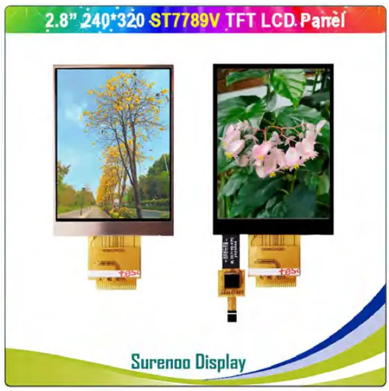
SHP0280A-240320-TN/IPS-NTP/CTP Series
TFT LCD PANEL USER MANUAL
 Please click the following image to buy the sample
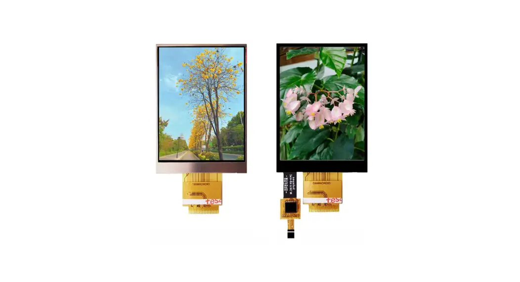
SHP0280A-240320 TFT LCD Display Screen Panel
 | http://www.surenoo.com;EMAIL:[email protected] |
 | https://wa.me/qr/4GGOIDYZ2PXXN1 |
 | https://u.wechat.com/EAK0B_l2YfPLwx3tRqiKkf4 |
 | https://line.me/ti/p/oas8BmVLVd |
 | https://u.wechat.com/EAK0B_l2YfPLwx3tRqiKkf4 |
Shenzhen Suero Technology Co.,Ltd.
www.surenoo.com
Skype: Surenoo365
Reference Controller Datasheet
TFT LCD Panel Selection Guide
ST7789
General Description
| MODEL NO | SHP0280A-240320-NTP/SHP0280A-240320-CTP |
| Display Mode | Transmissive |
| Display Format | Graphic 24ORGB*320 Dot-matrix 240XRGBx320 |
| Input Data | 4 Line-SPI interface |
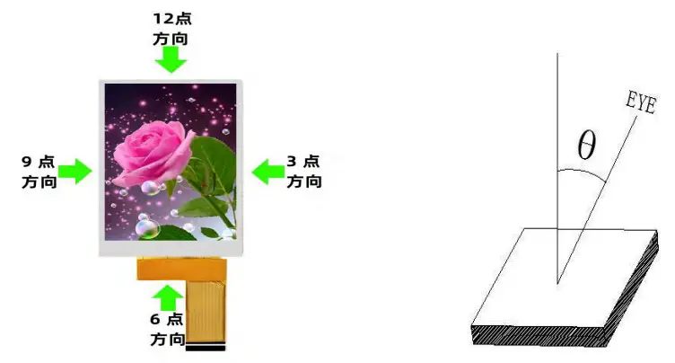
| Viewing Direction | TN: 12o’clock 12 IPS: All |
| Drive | ST7789V CTP: GT911 |
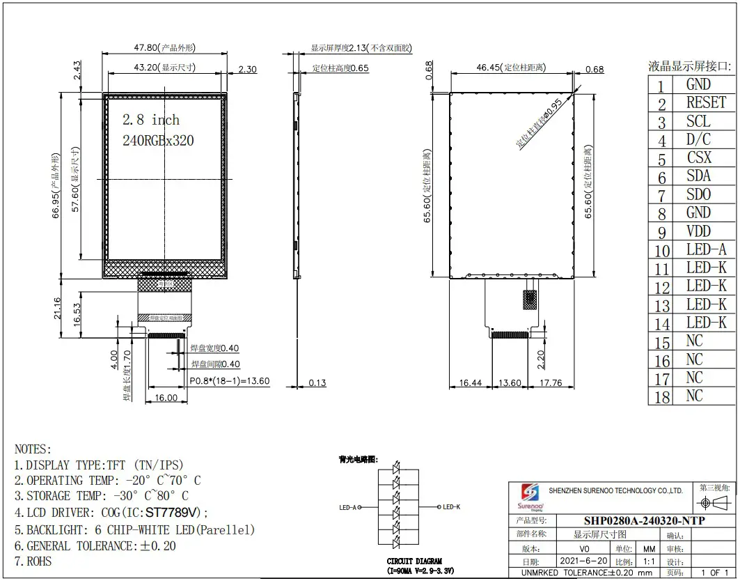
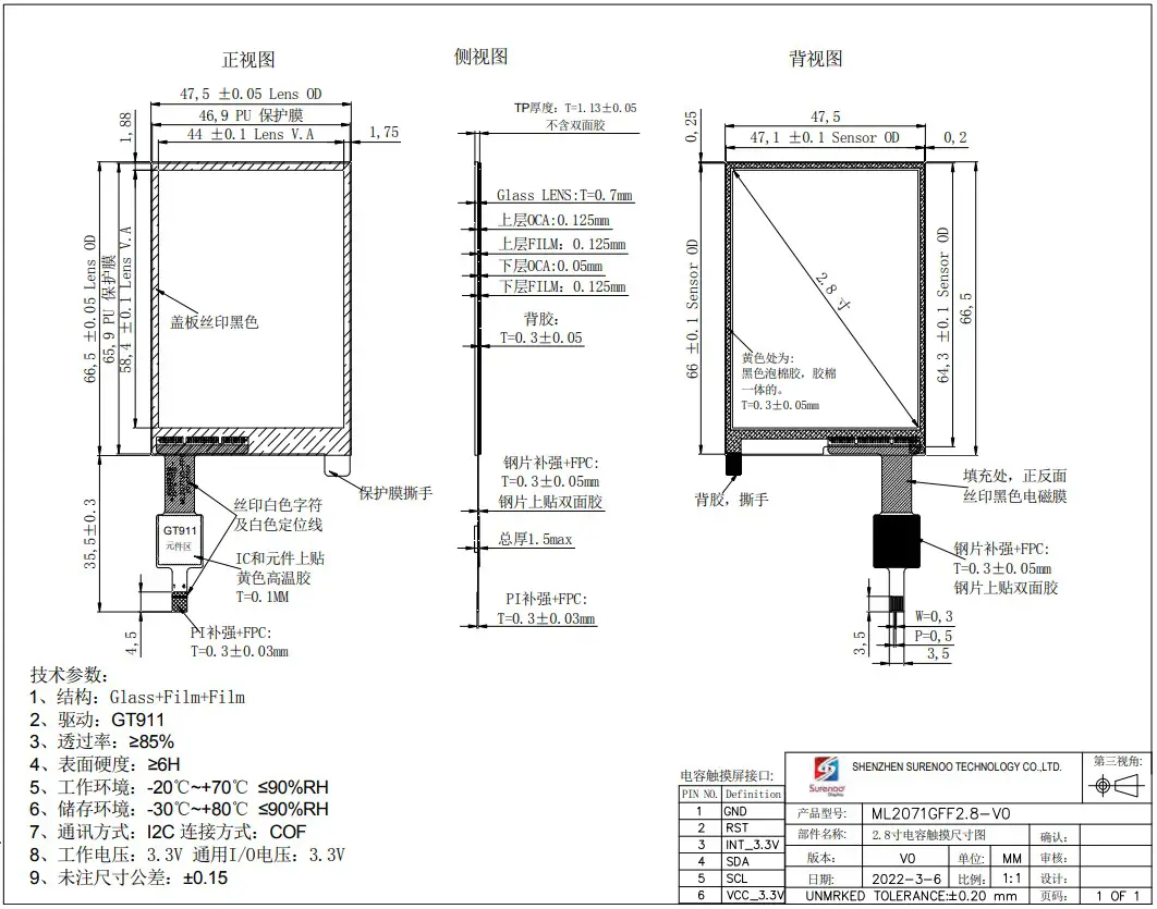
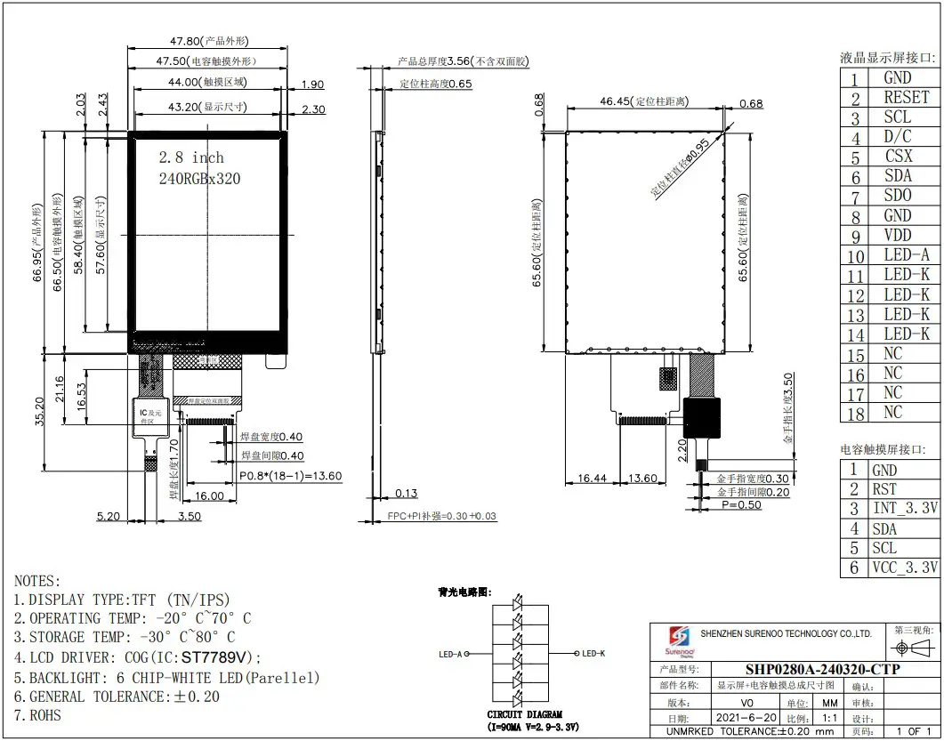
Mechanical Specification
| Item | Specifications | Unit |
| Dimensional outline | 47.80(W)*66.95(H)*2.13(T) (NTP) 47.80(W)*66.95(H)*3.56(T) (CTP) (FPC not include) | mm |
| Resolution | 24ORGB*320 | dot,, |
| LCD Active area | 43.20(W)*57.60 (H) | mm |
| Pixel size | 0.18W)*0.18(H) | mm |
Mechanical Dimension
TFT LCD Panel
Capacitive Touch Panel
TFT LCD Panel + Touch Panel
Electrical Maximum Ratings
| Item | Symbol | Min | \lax | l nit | Note |
| Supply voltage (VDDI) | V | 2. | 3. | – | |
| Supply voltage (VDD) | V | 3. | 3. | – | |
| Operating temperature I | Top | -20 | 70 | 0 | – |
5. Brightness characteristic & Power dissipation
| Item | Symbol | Min | Typical | Max | Unit |
| LED module Forward voltage | \fun | 3.0 | 3. | 3. | |
| LED module current | lune | – | 90 | – | mina |
| LCD Surface Luminance | Ls | 270 | 290 | – | Cd/m2 |
| LCM Surface brightness uniform | Li> | 80 | – | – | % |
| LCD power dissipation | Pi.cn | – | 0.33 | – | W |
*NOTE :PLCD=VDD * (ILED+ILCD)
Module Function Description
| PIN No. | Symbol | Description | Notes |
| 1 | GND | Ground | – |
| 2 | RESET | -This signal will reset the device and it must be applied to properly initialize the chip. -Signal is active low. | – |
| 3 | SCL | -This pin is used to be serial interface clock. | _ |
| 4 | 1)/C | – Display data/command selection pin in 4-line serial interface. | _ |
| 5 | CSX | -Chip selection pin Low enable. High disable. | _ |
| 6 | SDA | SPI interface input pin. -The data is latched on the rising edge of the SCL signal. -If not used, please fix this pin at VDDI or DGND level. | _ |
| 7 | SDO | -SPI interface output pin. -The data is output on the falling edge of the SCL signal. -If not used, let this pin open. | _ |
| 8 | GND | Ground | _ |
| 9 | VDD | Power Supply for Analog, Digital System and Booster Circuit. | – |
| 10 | LIMA | Anode of Backlight (2.9V-3.3V Typical:3.1V) | |
| 11 | IEDIC1 | Cathode of Backlight | – |
| 12 | LEDK2 | Cathode of Backlight | – |
| LEDK3 | Cathode of Backlight | – | |
| 14 | LEDK4 | Cathode of Backlight | – |
| 15 | XL | Touch panel Logical foot | _ |
| 16 | It | Touch panel Logical foot | – |
| 17 | 30I | Touch panel Logical foot | _ |
| 18 | I) | Touch panel Logical foot | _ |
CTP Interface Description
GT911 Touch Controller
| NO. | Symbol | I/O | DESCRIPTION |
| I | GND | Power supply | Power ground |
| 2 | RESET | I | CTP external reset signal, Low is active |
| 3 | INT 3.3 V | 0 | CTP External interrupt to the host |
| 4 | SDA | I/O | CTP 12C data input and output |
| 5 | SCL | I | CTP 12C clock input |
| 6 | VCC 3.3V | Power supply | CTP Power input |
Response time & Contrast ratio
| Item | Symbol | Condition | Remark | Unit | ||
| Min. | Typ. | Max. | ||||
| Response time | Trot | 0 =00 | – | 25 | 40 | ms |
| Contrast ratio | CR | 0 –0° | 350 | 500 | – | – |
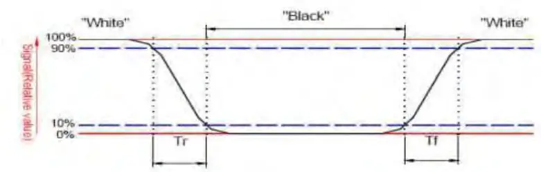
Contrast ratio (CR)= Brightness on the “white” state Brightness on the “black” state
Viewing Angle
TN Display
| Item | Symbol | Condition | Remark | Unit | ||
| Min. | Typ. | Max. | ||||
| Viewing angle | Top | CR?-:10 | 40 | 50 | – | Doff. |
| Bottom | CR.?-’10 | 55 | 65 | – | ||
| Left | CRS 10 | 55 | 65 | – | ||
| Right | CRS 10 | 55 | 65 | – | ||
IPS Display
| Item | Symbol | Condition | Remark | Unit | ||
| Min. | Typ. | Max. | ||||
| Viewing angle | Top | CR_.?/-10 | 80 | – | Deg. | |
| Bottom | CR..?-.10 | 80 | ||||
| Left | CR-?-10 | – | 80 | |||
| Right | Cit_.?/-10 | – | 80 | – | ||
Reliability Tria
| NO. | ITEM | CONDITION | CRITERION |
| High Temperature Non-Operating Test | 80°C | No Defect Of Operational Function In Room Temperature Are Allowable | |
| 2 | Low Temperature Non-Operating Test | -30°C*120Hrs | |
| High Temperature/Humidity Non Operating Test | 60°C*90%RH*120Hrs | ||
| 4 | High Temperature Operating Test | 70°C*72Hrs | |
| 5 | Low Temperature Operating Test | -20°C*72Hrs | |
| 6 | Thermal Shock Test | -20 t (30Mi n) Q 70 °C (30Min) *10CYCLES |
Inspection standards
Glass defect
| NO | Defect item | Criteria | Remark |
| I | Dimension Unconformity (Major defect) | By Engineering Drawing | |
| (-1 | Cracks (Major defect) | 1.Linear cracks panel [Reject] 2.Nonlinear crack contrast by limited sample | 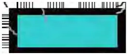 |
| 3 | Glass extrude the conductive area (minor defect) | a: disregards and no influence assemblage. 1) 1)—1/3Pin width(non bonding area) [Accept] 2)bonding area–.0. 5mm [Accept] | A: Length, b: Width |
| 4 | Pin-side ,conductive area damaged (minor defect) | (a c: disregards) bC-1/3of effective length for bonding electrode [Accept] | a: length, b: Width, c: Thickness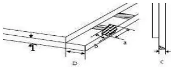 |
| 5 | Pin-side, on-conductive area damaged (minor defect) | 1)Damage area don’t touch the ITO (Inclueling contraposition mark, except scribing mark) [Accept ] 2)CC b BM1 /3of width [Accept ] 3)c=T b not touch the seal glue [Accept] 4)a disregards | a: Length, b: Width c: Thickness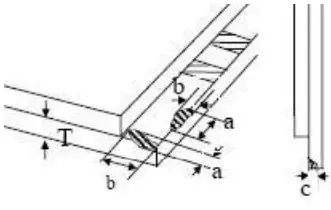 |
| 6 | Non-pin-side damage (minor defect) | c,<T I )b exceeds l/3Bm [Reject] c=T b not touch the seal glue [Reject] | c: Thickness b: width of damage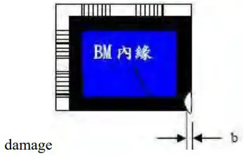 |
LCD appearance defect(View area)
| NO | Defect item | Criteria | Remark | |
| Fiber, glass crutch, polarizer scratch/folded (minor defect) | Specification | Allowable | notel:L: Length, W: Width note2: disregard if out of AA | |
| Noise 0.03mm | disregard | |||
| 0.03mm<W O. 05mm; I.; 3. Ohm | 2 | |||
| 0.05mm<W O. lemma; L Ohm | I | |||
| W>0.1mm;L>3.0nun | 0 | |||
| 2 | Polarizer bubble, concave and convex (minor defect) | 4 0.2mm | disregard | note 1: 4) = (L+W) /2, L :Length, W :Width note2:disregard if out of AA |
| 0.2nun< 4) O. 3mm | 2 | |||
| 0.3mm< 4 0. 5mm | 1 | |||
| 0.5mm< 4) | 0 | |||
| 3 | Black dots, dirty dots, | 4 0.15mm | disregard | note2:disregard if out of AA |
| impurities, eye winker (minor defect) | 0.15mm< 4 0. 25mm |  | ||
| 0.25mm< 4 0. 3m | I | |||
| 0.3mm< d) | 0 | |||
| 4 | Polarizer prick (minor defect) | 4 0.1 mm | disregard | note 1: d) = (L+W) /2, L=Length, W=Width note2:the distance between two dots>5mm |
| 0.1nun< 4) 0. 25mm | 3 | |||
| 40 >0. 25mm | 0 |
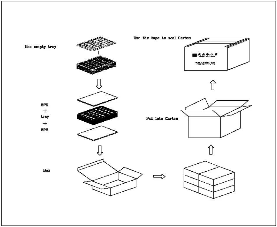
Package Method