Fibocom FG360-NA 5G Smart Module
Copyright
Copyright © 2021 Fibocom Wireless Inc. All rights reserved.
Without the prior written permission of the copyright holder, any company or individual is prohibited to excerpt, copy any part of or the entire document, or distribute the document in any form.
Notice
The document is subject to update from time to time owing to the product version upgrade or other reasons. Unless otherwise specified, the document only serves as the user guide. All the statements, information and suggestions contained in the document do not constitute any explicit or implicit guarantee.
Trademark
![]() The trademark is registered and owned by Fibocom Wireless Inc.
The trademark is registered and owned by Fibocom Wireless Inc.
Foreword
Introduction
The document describes the electrical characteristics, RF performance, dimensions and application environment, etc. of FG360-NA (hereinafter referred to as FG360). With the assistance of the document and other instructions, the developers can quickly understand the hardware functions of FG360 modules and develop products.
Overview
Introduction
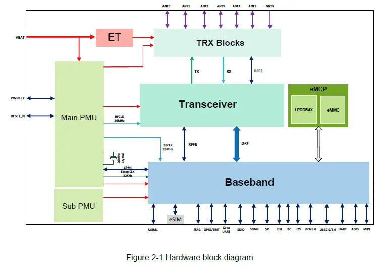
The FG360 series module is a 5G module which supports NSA and SA network architectures. The FG360 integrates core devices such as Baseband, Memory, PMU, Transceiver, and PA. It supports 5G NR Sub6, FDD-LTE, and TDD-LTE long-distance communication modes. Supports uplink 2×2 MIMO and downlink 4×4 MIMO multi-antenna configuration in SA mode. It also supports GNSS wireless positioning technology. The FG360 is designed in an LGA package and is suitable for a variety of eMBB scenarios, such as CPE, VR/AR, gateway, TV box, and intelligent monitoring.
Key Features
Table 2-1 Key features
| Performance | Description |
|
Operating Band | LTE FDD: B2, B4, B5, B12, B66, B71 |
| LTE TDD: B41, B46 | |
| NR: n25, n41, n66, n71 | |
| GNSS | Support GPS, GLONASS, Galileo, BDS, QZSS |
| NR | 3GPP Release 15 |
| LTE | 3GPP Release 15 |
|
Feature | NR: DL 4×4 MIMO: n25, n41, n66, n71 UL 2×2MIMO: n41
LTE: DL 4×4MIMO: B2, B4, B41 ,B66, B71 |
| NSA and SA supported | ||
| SRS: n41, Support: 1T2R, 1T4R, 2T4R | ||
| HPUE: B41, n41 | ||
|
Data Transmission | SA 5G/NR Sub-6 Peak | DL 4.43Gbps/UL 1.25Gbps |
| NSA Peak | DL 3.74Gbps/UL 700Mbps | |
| LTE | DL 1.6Gbps (CAT19)/UL 211Mbps (CAT18) | |
| Power Supply | DC: 3.3~4.4V, typical voltage: 3.8V | |
|
Temperature | Normal operating temperature: -30~75℃1 Extended operating temperature: -40~85℃2 Storage temperature: -40~85℃ | |
| Physical characteristics | Dimension: 41 mm×44mm×2.75 mm Package: 430 pin LGA Weight: about 12.0 g | |
| CPU | ARM Cortex-A55, quad core, up to 2.0 GHz | |
| Memory | 2GB LPDDR4x+32GB eMMC Flash | |
| Interface | ||
| USB Interface | USB2.0 high speed (HS) interface, data transmission rate up to 480Mbps USB3.0 Super-speed (SS) interface, data transmission rate up to 5Gbps | |
| PCIe Interface | PCIe Gen3 2Lane×1, PCIe Gen3 1Lane×2 (PCIe only support RC mode) | |
| SIM Interface | Dual SIM: 1.8V/3V SIM1: USIM SIM2: ESIM/USIM | |
| I2C | One set of I2C interface, data transmission rate up to 400Kbit/s | |
| ADCs | A/D conversion channel, Voltage Range: 0~1.45V | |
| Software | ||
| Firmware update | USB/PCIe/FOTA | |
| Operating System | Linux/Android/Windows | |
Note:
- When the temperature keeps in the range of -30~75°C, the module can work normally. Module performance meets the 3GPP specifications.
- When temperature keeps in the range of -40~85°C, module performance may be slightly out of 3GPP specifications.
Application Framework
The application framework below shows the main hardware functions of the FG360 module:
- Baseband
- RF transceiver
- PMU
- Memory
- Peripheral interface

Antenna Configuration
FG360 module supports seven antennas and the configuration is as below table:
| PAD | Function Description | Band Configuration(TX) | Band Configuration(RX) | Frequency Range(MHz) |
| 130 | LB TRX MHB sec TRX | B4/5/12/66/71 n25/41/66/71 | B2/4/5/12/41/66/71 n25/41/66/71 | 617~2690 |
| 175 | MHB TRX LAA RX LB RX | B2/4/41/66 n25/41/66 | B2/4/41/46/66/71 n25/41/66/71 | 617~5925 |
| 157 | MHB/LAA Rx | Only SRS | B2/4/41/46/66/71 n25/41/66/71 | 617~5925 |
| 139 | LMHB Rx | Only SRS | B2/4/5/12/41/66/71 n25/41/66/71 | 617~2690 |
| 148 | Reserved | |||
| 193 | Reserved | |||
| 199 | GNSS | GNSS receive |
Warning
Important Notice to OEM integrators
- This module is limited to OEM installation ONLY.
- This module is limited to installation in fixed applications, according to Part 2.1091(b).
- The separate approval is required for all other operating configurations, including portable configurations with respect to Part 2.1093 and different antenna configurations
- For FCC Part 15.31 (h) and (k): The host manufacturer is responsible for additional testing to verify compliance as a composite system. When testing the host device for compliance with Part 15 Subpart B, the host manufacturer is required to show compliance with Part 15 Subpart B while the transmitter module(s) are installed and operating. The modules should be transmitting and the evaluation should confirm that the module’s intentional emissions are compliant (i.e. fundamental and out of band emissions). The host manufacturer must verify that there are no additional unintentional emissions other than what is permitted in Part 15 Subpart B or emissions are compliant with the transmitter(s) rule(s). The Grantee will provide guidance to the host manufacturer for Part 15 B requirements if needed.
Important Note
notice that any deviation(s) from the defined parameters of the antenna trace, as described by the instructions, require that the host product manufacturer must notify to Fibocom Wireless Inc. that they wish to change
the antenna trace design. In this case, a Class II permissive change application is required to be filed by the USI, or the host manufacturer can take responsibility through the change in FCC ID (new application) procedure followed by a Class II permissive change application.
End Product Labeling
When the module is installed in the host device, the FCC/IC ID label must be visible through a window on the final device or it must be visible when an access panel, door or cover is easily re-moved. If not, a second label must be placed on the outside of the final device that contains the following text: “Contains FCC ID: ZMOFG360NA05”
The FCC ID can be used only when all FCC mpliance requirements are met.
Antenna Installation
- The antenna must be installed such that 20 cm is maintained between the antenna and users,
- The transmitter module may not be co-located with any other transmitter or antenna.
- Only antennas of the same type and with equal or less gains as shown below may be used with this module. Other types of antennas and/or higher gain antennas may require additional authorization for operation.
- The max allowed antenna gain is 3.76dBi for external monopole antenna.
In the event that these conditions cannot be met (for example certain laptop configurations or co-location with another transmitter), then the FCC authorization is no longer considered valid and the FCC ID/IC ID cannot be used on the final product. In these circumstances, the OEM integrator will be responsible for re-evaluating the end product (including the transmitter) and obtaining a separate FCC/IC authorization.
Manual Information to the End User
The OEM integrator has to be aware not to provide information to the end user regarding how to install or remove this RF module in the user’s manual of the end product which integrates this module. The end user manual shall include all required regulatory information/warning as show in this manual.
FCC Statement
Federal Communication Commission Interference Statement
This device complies with Part 15 of the FCC Rules. Operation is subject to the following two conditions: (1) This device may not cause harmful interference, and (2) this device must accept any interference received, including interference that may cause undesired operation.
This equipment has been tested and found to comply with the limits for a Class B digital device, pursuant to Part 15 of the FCC Rules. These limits are designed to provide reasonable protection against harmful interference in a residential installation. This equipment generates, uses and can radiate radio frequency energy and, if not installed and used in accordance with the instructions, may cause harmful interference to radio communications. However, there is no guarantee that interference will not occur in a particular installation. If this equipment does cause harmful interference to radio or television reception, which can be determined by turning the equipment off and on, the user is encouraged to try to correct the interference by one of the following measures:
- Reorient or relocate the receiving antenna.
- Increase the separation between the equipment and receiver.
- Connect the equipment into an outlet on a circuit different from that to which the receiver is connected.
- Consult the dealer or an experienced radio/TV technician for help.
Any changes or modifications not expressly approved by the party responsible for compliance could void the user’s authority to operate this equipment. This transmitter must not be co-located or operating in conjunction with any other antenna or transmitter.
This device is intended only for OEM integrators under the following conditions: (For module device use)
- The antenna must be installed such that 20 cm is maintained between the antenna and users, and
- The transmitter module may not be co-located with any other transmitter or antenna.
As long as 2 conditions above are met, further transmitter test will not be required. However, the OEM integrator is still responsible for testing their end-product for any additional compliance requirements required with this module installed.
Radiation Exposure Statement
This equipment complies with FCC radiation exposure limits set forth for an uncontrolled environment. This equipment should be installed and operated with minimum distance 20 cm between the radiator & your body.
Pin Definition
The FG360 module applies LGA interface with 430 pins.
Pin Map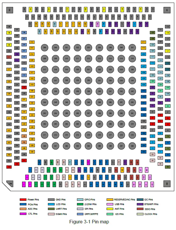
Note: The pin “RESERVED” means that the position pin is reserved and does not need to be connected.
Table of Pin No. and Pin Name
Table 3-1 Table of pin no. and pin name
| No. | PIN Name | No. | PIN Name | No. | PIN Name | No. | PIN Name | No. | PIN Name |
| 1 | PWRKEY | 2 | PON_1 | 3 | CLK_OUT | 4 | SYS_RESIN_N | 5 | SPI0_MISO |
| 6 | SPI0_CSB | 7 | SIM1_VDD | 8 | SPI0_MOSI | 9 | SPI0_CLK | 10 | SIM1_DATA |
| 11 | SIM2_RST | 12 | SIM2_DATA | 13 | SIM1_CLK | 14 | SIM1_DET | 15 | SIM2_CLK |
| 16 | SIM1_RST | 17 | SGMII_1_TXN | 18 | SIM2_VDD | 19 | GND | 20 | SGMII_1_TXP |
| 21 | SGMII_0_TXP | 22 | SGMII_1_RXN | 23 | RESERVED | 24 | SGMII_0_TXN | 25 | SGMII_1_RXP |
| 26 | PCIE_B_LN0_TXN | 27 | EINT17 | 28 | GBE0_RST | 29 | PCIE_B_LN0_TXP | 30 | PCIE_B_LN0_RXP |
| 31 | GND | 32 | RESERVED | 33 | PCIE_B_LN0_RXN | 34 | PCIE_A_CLKN | 35~36 | GND |
| 37 | PCIE_A_CLKP | 38 | PCIE_D_LN0_TXP | 39 | PCIE_D_LN0_TXN | 40 | PCIE_A_LN0_TXN | 41 | PCIE_D_LN0_RXP |
| 42 | GND | 43 | PCIE_A_LN0_TXP | 44 | PCIE_D_LN0_RXN | 45 | SDC_CLK | 46 | PCIE_A_LN0_RXN |
| 47 | SDC_CMD | 48 | RESERVED | 49 | PCIE_A_LN0_RXP | 50 | GND | 51 | SDC_DATA2 |
| 52 | GND | 53 | SDC_DATA1 | 54 | SDC_DATA3 | 55 | SSUSB_TXN | 56 | SDC_DATA0 |
| 57 | VBUS_DET | 58 | SSUSB_TXP | 59 | USB_DM | 60 | USB_ID | 61 | SSUSB_RXN |
| 62 | USB_DP | 63 | SSUSB_RXP | 64 | AP_URTS1 | 65 | GBE1_INT | 66 | MDC |
| 67 | PCIE_B_PEWAKEN | 68 | G3BE1_RST | 69 | MDIO | 70 | PCIE_B_CLKREQN | 71 | LSCE0B |
| 72 | LSDA | 73 | AP_URXD1 | 74 | LSDI | 75 | LSA0 | 76 | PCIE_B_PERSTN |
| 77 | AP_UTXD1 | 78 | LRSTB | 79 | AP_UCTS1 | 80 | LSCK | 81~83 | GND |
| 84~89 | VBAT_RF | 90~92 | GND | 93 | PCM0_SYNC | 94 | I2S0_MCK | 95 | PCM0_DI |
| 96 | PCM0_CLK | 97 | PCM0_DO | 98 | CDC_RESET_N | 99 | PTA_TX | 100 | CDC_INT1_N |
| 101 | I2S0_BCK | 102 | PTA_RX | 103 | I2S0_DO | 104 | I2S0_DI | 105 | I2S0_LRCK |
| 106 | NET_STATUS | 107 | AUDIO_PWR_EN | 108 | STATUS | 109 | W_DISABLE | 110 | NET_MODE |
| 111 | SLEEP_IND | 112 | I2C_SCL0 | 113 | WAKEUP_IN | 114 | ISINK1 | 115 | I2C_SDA0 |
| 116 | ANTCTL3 | 117 | IRIG_B | 118~119 | GND | 120 | GPS_PPS | 121 | NC |
| 122 | GND | 123 | EINT20 | 124~125 | GND | 126 | DBG_UART_RX | 127~128 | GND |
| 129 | DBG_UART_TX | 130 | ANT8_M | 131~134 | GND | 135 | BT_UTXD | 136~137 | GND |
| 138 | BT_URXD | 139 | ANT7_D | 140 | GND | 141 | DSI_TE | 142~143 | GND |
| 144 | EINT16 | 145~147 | GND | 148 | ANT6 | 149 | GND | 150 | BT_PRI_RXD |
| 151~152 | GND | 153 | BT_ACT_TXD | 154~155 | GND | 156 | DISP_PWM | 157 | ANT5_M2 |
|
158 |
GND |
159 |
USB_DRVBUS |
160~161 |
GND |
162 | GPIO78/
PCIE_D_CLKREQN |
163~164 |
GND |
| No. | PIN Name | No. | PIN Name | No. | PIN Name | No. | PIN Name | No. | PIN Name |
| 165 | NC | 166 | NC | 167 | GND | 168 | NC | 169~170 | GND |
| 171 | NC | 172~173 | GND | 174 | NC | 175 | ANT3_M1 | 176 | GND |
| 177 | NC | 178~179 | GND | 180 | LCD_PWR_EN2 | 181~182 | GND | 183 | TDI |
| 184 | NC | 185 | GND | 186 | TCK | 187~188 | GND | 189 | TDO |
| 190~192 | GND | 193 | ANT1 | 194~197 | GND | 198 | MIPI1_D_SDATA | 199 | ANT10_GNSS |
| 200 | GND | 201 | MIPI1_D_SCLK | 202~203 | GND | 204 | ANTCTL2 | 205 | NC |
|
206 |
GND |
207 |
ANTCTL1 |
208 |
GND |
209 | GPIO76/
PCIE_D_PERSTN |
210 |
ANTCTL0 |
| 211 | SDIO_VDD | 212 | EINT15 | 213~215 | GND | 216 | MIPI2_D_SDATA | 217 | RESERVED |
| 218 | GND | 219 | MIPI2_D_SCLK | 220~222 | GND | 223 | RESERVED | 224 | GND |
| 225 | VDD_EXT_1V8 | 226~228 | GND | 229 | RESERVED | 230 | GND | 231 | NC |
| 232~234 | GND | 235 | RESERVED | 236 | GND | 237 | RESERVED | 238~239 | GND |
| 240~241 | RESERVED | 242 | GND | 243 | RESERVED | 244~245 | GND | 246~247 | RESERVED |
| 248 | GND | 249 | ADC0 | 250~251 | GND | 252 | ADC1 | 253 | RESERVED |
| 254 | GND | 255 | NC | 256~258 | GND | 259 | RESERVED | 260 | GND |
| 261 | VBAT_BB | 262 | GND | 263~264 | VBAT_BB | 265 | PCIE_D_CLKN | 266 | GND |
| 267 | SIM2_DET | 268 | SGMII_0_RXP | 269 | SGMII_0_RXN | 270 | SGMII_PWR_EN1 | 271 | PCIE_B_CLKP |
| 272 | PCIE_B_CLKN | 273 | USB_BOOT | 274 | PCIE_A_PEWAKEN | 275 | PCIE_A_PERSTN | 276 | PCIE_A_CLKREQN |
| 277 | GND | 278 | GBE0_INT | 279 | EINT18 | 280 | SDC_DET | 281 | SD_PWR_EN |
|
282 |
BT_URTS |
283 |
BT_UCTS |
284 |
GND |
285 | GPIO77/
PCIE_D_PEWAKEN |
286 |
WIFI_GPIO1 |
| 287 | WLAN_ACT | 288 | LCM_RST | 289 | GND | 290 | NC | 291 | WIFI_GPIO2 |
| 292 | NC | 293 | RESERVED | 294 | NC | 295 | TRST_N | 296 | TMS |
| 297 | SYSRSTB | 298 | LCD_PWR_EN1 | 299~392 | GND | 393 | PCIE_C_LN0_RXN | 394 | PCIE_C_LN0_RXP |
| 395 | PCIE_C_LN0_TXP | 396 | PCIE_C_LN0_TXN | 397~398 | GND | 399 | PCIE_C_CLKP | 400 | PCIE_C_CLKN |
| 401 | PCIE_C_PERSTN | 402 | PCIE_C_CLKREQN | 403 | PCIE_C_PEWAKEN | 404 | DSI0_D0P | 405 | DSI0_D0N |
| 406 | DSI0_CKN | 407 | DSI0_CKP | 408 | DSI0_D1N | 409 | DSI0_D1P | 410~425 | NC |
| 426 | RESERVED | 427 | RESERVED | 428 | RESERVED | 429 | RESERVED | 430 | RESERVED |
Pin Definition
Table 3-2 IO Parameter definition
| Type | Description |
| PI | Power Input |
| PO | Power Output |
| DI | Digital Input |
| DO | Digital Output |
| DIO | Digital Input/Output |
| AI | Analog Input |
| AO | Analog Output |
| AIO | Analog Input/Output |
| OD | Open Drain |
| PU | Internal pull up |
| PD | Internal pull down |
| Hi-Z | High impedance |
Table 3-3 LGA pin description
| Pin Name | Pin No. | Type | Power Domain | Reset Value | Pin Description |
| Power | |||||
| VBAT_BB | 261 263, 264 | PI | – | – | Baseband power input |
| VBAT_RF | 84, 85, 86, 87, 88, 89 | PI | – | – | RF power input |
| VDD_EXT_1V8 | 225 | PO | – | – | 1.8V power output |
| USB | |||||
| SSUSB_TXN | 55 | AO | – | – | USB super speed transmit data minus |
| SSUSB_TXP | 58 | AO | – | – | USB super speed transmit data plus |
| SSUSB_RXN | 61 | AI | – | – | USB super speed receive data minus |
| SSUSB_RXP | 63 | AI | – | – | USB super speed receive data plus |
| USB_DM | 59 | AIO | – | – | USB high speed data minus |
| USB_DP | 62 | AIO | – | – | USB high speed data plus |
| VBUS_DET | 57 | DI | – | – | USB VBUS detection |
| USB_DRVBUS | 159 | DO | VDD_EXT_1V8 | PD | USB OTG power enable |
| USB_ID | 60 | DI | VDD_EXT_1V8 | PD | USB ID |
| USIM | |||||
| Pin Name | Pin No. | Type | Power Domain | Reset Value | Pin Description |
| SIM1_VDD | 7 | PO | – | – | SIM1 power supply,3V/1.8V |
| SIM1_DATA | 10 | DIO | SIM1_VDD | PD | SIM1 data input/output |
| SIM1_CLK | 13 | DO | SIM1_VDD | PD | SIM1 clock signal |
| SIM1_RST | 16 | DO | SIM1_VDD | PD | SIM1 reset signal |
| SIM1_DET | 14 | DI | VDD_EXT_1V8 | PD | SIM1 detect signal |
| SIM2_VDD | 18 | PO | – | – | SIM2 power supply,3V/1.8V, Reserved |
| SIM2_DATA | 12 | DIO | SIM2_VDD | PD | SIM2 data input/output, Reserved |
| SIM2_CLK | 15 | DO | SIM2_VDD | PD | SIM2 clock signal, Reserved |
| SIM2_RST | 11 | DO | SIM2_VDD | PD | SIM2 reset signal, Reserved |
| SIM2_DET | 267 | DI | VDD_EXT_1V8 | PD | SIM2 detect, Reserved |
| GPIO | |||||
| W_DISABLE | 109 | DI | VDD_EXT_1V8 | PD | Module airplane mode control signal |
| WAKEUP_IN | 113 | DI | VDD_EXT_1V8 | PD | Module wake up input from host |
| NET_STATUS | 106 | DO | VDD_EXT_1V8 | PD | Module network status indication |
| NET_MODE | 110 | DO | VDD_EXT_1V8 | PD | Module network mode indication |
| SLEEP_IND | 111 | DO | VDD_EXT_1V8 | PD | Module output to wake up host |
| STATUS | 108 | DO | VDD_EXT_1V8 | PD | Module current working status indication |
| IRIG_B | 117 | DO | VDD_EXT_1V8 | PD | B code output |
| GPS_PPS | 120 | DO | VDD_EXT_1V8 | PD | PPS signal output |
| ISINK1 | 114 | AI | VBAT_BB | HI-Z | LED negative drive signal |
| ANT | |||||
| ANT1 | 193 | AIO | – | – | UCB TRx |
| NC | 184 | AIO | – | – | NC |
| ANT3_M1 | 175 | AIO | – | – | 41 TRx + MHB/UCB/LAA Rx |
| NC | 166 | AIO | – | – | NC |
| ANT5_M2 | 157 | AIO | – | – | MHB/UCB/LAA Rx |
| ANT6 | 148 | AIO | – | – | UCB TRx |
| ANT7_D | 139 | AIO | – | – | LMHB Rx |
| ANT8_M | 130 | AIO | – | – | LMH TRX |
| NC | 121 | AIO | – | – | NC |
| ANT10_GNSS | 199 | AI | – | – | GNSS antenna |
| NC | 205 | AIO | – | – | NC |
| ANT Tuner Control | |||||
| MIPI1_D_SDATA | 198 | DIO | VDD_EXT_1V8 | PD | External Tuner MIPI Control Data Pin |
| MIPI1_D_SCLK | 201 | DO | VDD_EXT_1V8 | PD | External Tuner MIPI Control Clock Pin |
| MIPI2_D_SDATA | 216 | DIO | VDD_EXT_1V8 | PD | External Tuner MIPI Control Data Pin |
| Pin Name | Pin No. | Type | Power Domain | Reset Value | Pin Description |
| MIPI2_D_SCLK | 219 | DO | VDD_EXT_1V8 | PD | External Tuner MIPI Control Clock Pin |
| ANTCTL0 | 210 | DO | 1.8V | PD | Antenna control signal 0 |
| ANTCTL1 | 207 | DO | 1.8V | PD | Antenna control signal 1 |
| ANTCTL2 | 204 | DO | 1.8V | PD | Antenna control signal 2 |
| ANTCTL3 | 116 | DO | 1.8V | PD | Antenna control signal 3 |
| Module Control | |||||
| PWRKEY | 1 | DI | 1.8V | PU | Module power-key control signal |
| SYS_RESIN_N | 4 | DI | 1.8V | PU | Module reset control signal |
| PON_1 | 2 | DI | ≤VBAT_BB | PU | Module power on signal |
| EINT20 | 123 | DI | VDD_EXT_1V8 | PD | MT6890 interruput input signal, used for WPS key input signal |
| USB_BOOT | 273 | DI | VDD_EXT_1V8 | PD | Force into USB download boot mode |
| SD | |||||
| SDC_CMD | 47 | DIO | SDIO_VDD | PD | SDC interface command signal |
| SDC_DATA1 | 53 | DIO | SDIO_VDD | PD | SDC interface DATA1 signal |
| SDC_DATA0 | 56 | DIO | SDIO_VDD | PD | SDC interface DATA0 signal |
| SDC_CLK | 45 | DO | SDIO_VDD | PD | SDC interface clock signal |
| SDC_DATA2 | 51 | DIO | SDIO_VDD | PD | SDC interface DATA2 signal |
| SDC_DATA3 | 54 | DIO | SDIO_VDD | PD | SDC interface DATA3 signal |
| SDC_DET | 280 | DI | VDD_EXT_1V8 | PD | SD card insert detection |
| SD_PWR_EN | 281 | DO | VDD_EXT_1V8 | PD | SD card power supply enable |
| SDIO_VDD | 211 | PO | – | – | SDC interface I/O power domain |
| SGMII | |||||
| SGMII_1_RXN | 22 | AIO | AVDD12_SGMI I | – | SGMII 1 receive data minus |
| SGMII_1_RXP | 25 | AIO | AVDD12_SGMI I | – | SGMII 1 receive data plus |
| SGMII_1_TXN | 17 | AIO | AVDD12_SGMI I | – | SGMII 1 transmit data minus |
| SGMII_1_TXP | 20 | AIO | AVDD12_SGMI I | – | SGMII 1 transmit data plus |
| GBE1_INT | 65 | DI | VDD_EXT_1V8 | PD | SGMII 1 interrupt input signal |
| GBE1_RST | 68 | DO | VDD_EXT_1V8 | PD | SGMII 1 reset signal |
| SGMII_0_RXN | 269 | AIO | AVDD12_SGMI I | – | SGMII 0 receive data minus |
| SGMII_0_RXP | 268 | AIO | AVDD12_SGMI I | – | SGMII 0 receive data plus |
| SGMII_0_TXN | 24 | AIO | AVDD12_SGMI I | – | SGMII 0 transmit data minus |
| SGMII_0_TXP | 21 | AIO | AVDD12_SGMI I | – | SGMII 0 transmit data plus |
| Pin Name | Pin No. | Type | Power Domain | Reset Value | Pin Description |
| GBE0_INT | 278 | DI | VDD_EXT_1V8 | PD | SGMII 0 interrupt input signal |
| GBE0_RST | 28 | DO | VDD_EXT_1V8 | PD | SGMII 0 reset signal |
| SGMII_PWR_EN1 | 270 | DO | VDD_EXT_1V8 | PD | SGMII power supply enable 1 |
| MDIO | 69 | DIO | VDD_EXT_1V8 | PD | SGMII MDIO signal |
| MDC | 66 | DO | VDD_EXT_1V8 | PD | SGMII MDC signal |
| PCIE | |||||
| PCIE_A_CLKN | 34 | AIO | AVDD12_PCIE | – | PCIe A reference clock minus |
| PCIE_A_CLKP | 37 | AIO | AVDD12_PCIE | – | PCIe A reference clock plus |
| PCIE_A_LN0_TXN | 40 | AIO | AVDD12_PCIE | – | PCIe A Tx0 minus |
| PCIE_A_LN0_TXP | 43 | AIO | AVDD12_PCIE | – | PCIe A Tx0 plus |
| PCIE_A_LN0_RXN | 46 | AIO | AVDD12_PCIE | – | PCIe A Rx0 minus |
| PCIE_A_LN0_RXP | 49 | AIO | AVDD12_PCIE | – | PCIe A Rx0 plus |
| PCIE_A_PEWAKEN | 274 | DI | VDD_EXT_1V8 | PU | PCIe A wake-up signal |
| PCIE_A_PERSTN | 275 | DO | VDD_EXT_1V8 | PU | PCIe A reset signal |
| PCIE_A_CLKREQN | 276 | DIO | VDD_EXT_1V8 | PU | PCIe A clock request signal |
| PCIE_B_CLKN | 272 | AIO | AVDD12_PCIE | – | PCIe B reference clock minus |
| PCIE_B_CLKP | 271 | AIO | AVDD12_PCIE | – | PCIe B reference clock plus |
| PCIE_B_LN0_TXN | 26 | AIO | AVDD12_PCIE | – | PCIe B Tx0 minus |
| PCIE_B_LN0_TXP | 29 | AIO | AVDD12_PCIE | – | PCIe B Tx0 plus |
| PCIE_B_LN0_RXN | 33 | AIO | AVDD12_PCIE | – | PCIe B Rx0 minus |
| PCIE_B_LN0_RXP | 30 | AIO | AVDD12_PCIE | – | PCIe B Rx0 plus |
| PCIE_B_PEWAKEN | 67 | DI | VDD_EXT_1V8 | PU | PCIe B wake-up signal |
| PCIE_B_PERSTN | 76 | DO | VDD_EXT_1V8 | PU | PCIe B reset signal |
| PCIE_B_CLKREQN | 70 | DIO | VDD_EXT_1V8 | PU | PCIe B clock request signal |
| PCIE_C_CLKN | 400 | AIO | AVDD12_PCIE | – | PCIe C reference clock minus |
| PCIE_C_CLKP | 399 | AIO | AVDD12_PCIE | – | PCIe C reference clock plus |
| PCIE_C_LN0_TXN | 396 | AIO | AVDD12_PCIE | – | PCIe C Tx0 minus |
| PCIE_C_LN0_TXP | 395 | AIO | AVDD12_PCIE | – | PCIe CTx0 plus |
| PCIE_C_LN0_RXN | 393 | AIO | AVDD12_PCIE | – | PCIe C Rx0 minus |
| PCIE_C_LN0_RXP | 394 | AIO | AVDD12_PCIE | – | PCIe C Rx0 plus |
| PCIE_C_PEWAKEN | 403 | DI | VDD_EXT_1V8 | PU | PCIe C wake-up signal |
| PCIE_C_PERSTN | 401 | DO | VDD_EXT_1V8 | PU | PCIe C reset signal |
| PCIE_C_CLKREQN | 402 | DIO | VDD_EXT_1V8 | PU | PCIe C clock request signal |
| PCIE_D_CLKN | 3 | AIO | AVDD12_PCIE | – | PCIe D reference clock minus, Reserved |
| PCIE_D_CLKP | 265 | AIO | AVDD12_PCIE | – | PCIe D reference clock plus, Reserved |
| PCIE_D_LN0_TXN | 39 | AIO | AVDD12_PCIE | – | PCIe D Tx0 minus, Reserved |
| PCIE_D_LN0_TXP | 38 | AIO | AVDD12_PCIE | – | PCIe D Tx0 plus, Reserved |
| PCIE_D_LN0_RXN | 44 | AIO | AVDD12_PCIE | – | PCIe D Rx0 minus, Reserved |
| PCIE_D_LN0_RXP | 41 | AIO | AVDD12_PCIE | – | PCIe D Rx0 plus, Reserved |
| GPIO76/ PCIE_D_PERSTN | 209 | DI | VDD_EXT_1V8 | PD | MT6890 GPIO, used for 2+2+4 and 4+4+4 WIFI/BT and RF co-exist control signals |
| GPIO77/ PCIE_D_PEWAKEN | 285 | DO | VDD_EXT_1V8 | PD | MT6890 GPIO, used for 2+2+4 and 4+4+4 WIFI/BT |
| Pin Name | Pin No. | Type | Power Domain | Reset Value | Pin Description |
| and RF co-exist control signals | |||||
| GPIO78/ PCIE_D_CLKREQN | 162 | DO | VDD_EXT_1V8 | PD | MT6890 GPIO, used for 2+2+4 and 4+4+4 WIFI/BT and RF co-exist control signals |
| JTAG | |||||
| TDI | 183 | DI | VDD_EXT_1V8 | PD | JTAG TDI,Reserved |
| TCK | 186 | DI | VDD_EXT_1V8 | PD | JTAG TCK,Reserved |
| TDO | 189 | DO | VDD_EXT_1V8 | PD | JTAG TDO,Reserved |
| TRST_N | 295 | DI | VDD_EXT_1V8 | PD | JTAG TRST,Reserved |
| TMS | 296 | DI | VDD_EXT_1V8 | PD | JTAG TMS,Reserved |
| SYSRSTB | 297 | DI | VDD_EXT_1V8 | PD | System reset,Reserved |
| I2C | |||||
| I2C_SDA0 | 115 | DIO | VDD_EXT_1V8 | PU | I2C data |
| I2C_SCL0 | 112 | DO | VDD_EXT_1V8 | PU | I2C clock |
| I2S | |||||
| I2S0_DO | 103 | DO | VDD_EXT_1V8 | PD | I2S data output signal |
| I2S0_MCK | 94 | DO | VDD_EXT_1V8 | PD | I2S clock output signal |
| I2S0_DI | 104 | DI | VDD_EXT_1V8 | PD | I2S data input signal |
| I2S0_BCK | 101 | DO | VDD_EXT_1V8 | PD | I2S data bit clock signal |
| I2S0_LRCK | 105 | DO | VDD_EXT_1V8 | PD | I2S frame clock signal |
| ADC | |||||
| ADC0 | 249 | AI | VDD_EXT_1V8 | – | A/D conversion channel 0 |
| ADC1 | 252 | AI | VDD_EXT_1V8 | – | A/D conversion channel 1 |
| Debug UART | |||||
| DBG_UART_TX | 129 | DO | VDD_EXT_1V8 | PU | Debug UART data transmission |
| DBG_UART_RX | 126 | DI | VDD_EXT_1V8 | PU | Debug UART data reception |
| UART | |||||
| AP_UCTS1 | 79 | DI | VDD_EXT_1V8 | PD | UART receive ready signal |
| AP_URTS1 | 64 | DO | VDD_EXT_1V8 | PD | UART transmit request signal |
| AP_UTXD1 | 77 | DO | VDD_EXT_1V8 | PD | UART transmit signal |
| AP_URXD1 | 73 | DI | VDD_EXT_1V8 | PD | UART receive signal |
| SPI | |||||
| SPI0_MISO | 5 | DI | VDD_EXT_1V8 | PD | SPI interface input signal |
| SPI0_MOSI | 8 | DO | VDD_EXT_1V8 | PD | SPI interface output signal |
| SPI0_CSB | 6 | DO | VDD_EXT_1V8 | PD | SPI interface chip select signal |
| SPI0_CLK | 9 | DO | VDD_EXT_1V8 | PD | SPI interface clock signal |
| AUDIO CODEC | |||||
| CDC_RESET_N | 98 | DO | VDD_EXT_1V8 | PD | External CODEC reset signal |
| CDC_INT1_N | 100 | DI | VDD_EXT_1V8 | PD | External CODEC interrupt signal |
| Pin Name | Pin No. | Type | Power Domain | Reset Value | Pin Description |
| AUDIO_PWR_EN | 107 | DO | VDD_EXT_1V8 | PD | External CODEC power enable |
| LCD | |||||
| LSCK | 80 | DO | VDD_EXT_1V8 | PD | CLK signal for DBI-C serial 3/4 wire SPI LCD, connect to LCD CLK signal |
|
LSDA |
72 |
DO/DI |
VDD_EXT_1V8 |
PD | Data signal for DBI-C serial 3/4 wire SPI LCD. For type interface I LCD, is data input/output signal. For type interface II LCD, is data output signal from FG360 module and connect to LCD data in signal |
| LSA0 | 75 | DO | VDD_EXT_1V8 | PD | RS signal for DBI-C serial 4 wire SPI LCD, DBI-C serial 3 wire SPI LCD not has this signal |
| LSCE0B | 71 | DO | VDD_EXT_1V8 | PD | CS signal for DBI-C serial 3/4 wire SPI LCD, connect to LCD CS signal |
|
LSDI |
74 |
DI |
VDD_EXT_1V8 |
PD | Data signal for DBI-C serial 3/4 wire SPI LCD. For type interface II LCD, is data input signal from FG360 module and connect to LCD data output signal. For type interface I LCD, not has this signal |
| LRSTB | 78 | DO | VDD_EXT_1V8 | PD | Reset signal for DBI-C serial 3/4 wire SPI LCD, connect to LCD RST signal |
| DSI_TE | 141 | DI | VDD_EXT_1V8 | PD | LCD frame synchronization signal |
| DISP_PWM | 156 | DO | VDD_EXT_1V8 | PD | LCD Backlight control PWM signal |
| LCM_RST | 288 | DO | VDD_EXT_1V8 | PD | DSI LCD reset signal |
| LCD_PWR_EN1 | 298 | DO | VDD_EXT_1V8 | PD | LCD power supply enable 1 |
| LCD_PWR_EN2 | 180 | DO | VDD_EXT_1V8 | PD | LCD power supply enable 2 |
| DSI0_CKN | 406 | AIO | AVDD12_DSI | – | DSI LCD MIPI CLK minus |
| DSI0_CKP | 407 | AIO | AVDD12_DSI | – | DSI LCD MIPI CLK plus |
| DSI0_D0N | 405 | AIO | AVDD12_DSI | – | DSI LCD MIPI lane0 minus |
| DSI0_D0P | 404 | AIO | AVDD12_DSI | – | DSI LCD MIPI lane0 plus |
| DSI0_D1N | 408 | AIO | AVDD12_DSI | – | DSI LCD MIPI lane1 minus |
| DSI0_D1P | 409 | AIO | AVDD12_DSI | – | DSI LCD MIPI lane1 plus |
| WIFI/BT | |||||
| BT_UTXD | 135 | DO | VDD_EXT_1V8 | PD | UART TX signal |
| BT_URXD | 138 | DI | VDD_EXT_1V8 | PD | UART RX signal |
| Pin Name | Pin No. | Type | Power Domain | Reset Value | Pin Description |
| BT_URTS | 282 | DO | VDD_EXT_1V8 | PD | UART RTS signal |
| BT_UCTS | 283 | DI | VDD_EXT_1V8 | PD | UART CTS signal |
| PCM0_DO | 97 | DO | VDD_EXT_1V8 | PD | PCM data output |
| PCM0_DI | 95 | DI | VDD_EXT_1V8 | PD | PCM data input |
| PCM0_CLK | 96 | DO | VDD_EXT_1V8 | PD | PCM clock output |
| PCM0_SYNC | 93 | DO | VDD_EXT_1V8 | PD | PCM synchronization signal |
| EINT16 | 144 | DO | VDD_EXT_1V8 | PD | MT6890 GPIO, used for control WIFI RESET signal or WIFI Power enable signal |
| EINT17 | 27 | DO | VDD_EXT_1V8 | PD | MT6890 GPIO, used for control WIFI RESET signal or WIFI Power enable signal |
| EINT18 | 279 | DO | VDD_EXT_1V8 | PD | MT6890 GPIO, used for control WIFI RESET signal or WIFI Power enable signal |
| EINT15 | 212 | DI | VDD_EXT_1V8 | PD | Interrupt input signal, used as WLAN_EN |
| BT_PRI_RXD | 150 | DI | VDD_EXT_1V8 | PD | WIFI/BT and RF co-exist control signals |
| BT_ACT_TXD | 153 | DO | VDD_EXT_1V8 | PD | WIFI/BT and RF co-exist control signals |
| WLAN_ACT | 287 | DI | VDD_EXT_1V8 | PD | WIFI/BT and RF co-exist control signals |
| PTA_TX | 99 | DO | VDD_EXT_1V8 | PD | WIFI/BT and RF co-exist control signals |
| PTA_RX | 102 | DI | VDD_EXT_1V8 | PD | WIFI/BT and RF co-exist control signals |
| WIFI_GPIO1 | 286 | DIO | VDD_EXT_1V8 | PD | WIFI control signal 1, Reserved |
| WIFI_GPIO2 | 291 | DIO | VDD_EXT_1V8 | PD | WIFI control signal 2, Reserved |
| MMW | |||||
| NC | 237 | – | – | – | Reserved |
| NC | 223 | – | – | – | Reserved |
| NC | 217 | – | – | – | Reserved |
| NC | 240 | – | – | – | Reserved |
| NC | 235 | – | – | – | Reserved |
| NC | 229 | – | – | – | Reserved |
| NC | 243 | – | – | – | Reserved |
| NC | 247 | – | – | – | Reserved |
| NC | 241 | – | – | – | Reserved |
| NC | 246 | – | – | – | Reserved |
| NC | 259 | – | – | – | Reserved |
| NC | 253 | – | – | – | Reserved |
| Reserved | |||||
| RESERVED | 23, 32, 48, 293,426~430 | – | – | – | – |
| NC | |||||
| Pin Name | Pin No. | Type | Power Domain | Reset Value | Pin Description |
| NC | 165,168,171, 174,177,231, 255,290,292, 294,410~425 | – | – | – | – |
| Pin Name | Pin No. |
| GND | |
| 19, 31, 35, 36, 42, 50, 52, 81, 82, 83, 90, 91, 92, 118, 119, 122, 124, 125, 127, 128, 131, | |
| 132, 133, 134, 136, 137, 140, 142, 143, 145, 146, 147, 149, 151, 152, 154, 155, 158, 160, | |
| 161, 163, 164, 167, 169, 170, 172, 173, 176, 178, 179, 181, 182, 185, 187, 188, 190, 191, | |
| 192, 194, 195, 196, 197, 200, 202, 203, 206, 208, 213, 214, 215, 218, 220, 221, 222, 224, | |
| 226, 227, 228, 230, 232, 233, 234, 236, 238, 239, 242, 244, 245, 248, 250, 251, 254, 256, | |
| GND | 257, 258, 260, 262, 266, 277, 284, 289, 299, 300, 301, 302, 303, 304, 305, 306, 307, 308, 309, 310, 311, 312, 313, 314, 315, 316, 317, 318, 319, 320, 321, 322, 323, 324, 325, 326, |
| 327, 328, 329, 330, 331, 332, 333, 334, 335, 336, 337, 338, 339, 340, 341, 342, 343, 344, | |
| 345, 346, 347, 348, 349, 350, 351, 352, 353, 354, 355, 356, 357, 358, 359, 360, 361, 362, | |
| 363, 364, 365, 366, 367, 368, 369, 370, 371, 372, 373, 374, 375, 376, 377, 378, 379, 380, | |
| 381, 382, 383, 384, 385, 386, 387, 388, 389, 390, 391, 392, 397,398 | |
Note:
- The PWRKEY and SYS_RESIN_N pins have internal pull-up, and the pull-up power supply is in exclusive mode; no external pull-up is required; PON_1 pin module with weak pull-down, maximum input voltage must not exceed VBAT_BB.
Structural Specification
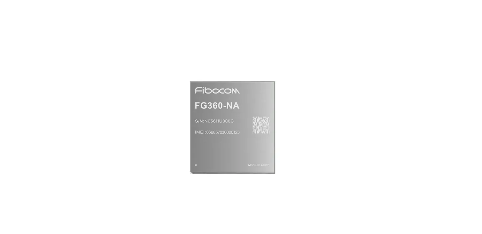
Product Appearance
The appearance of the FG360 module product is as shown: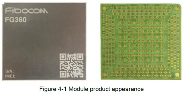
Dimension of Structure
The structural dimensions of the FG360 module are shown in the figure: 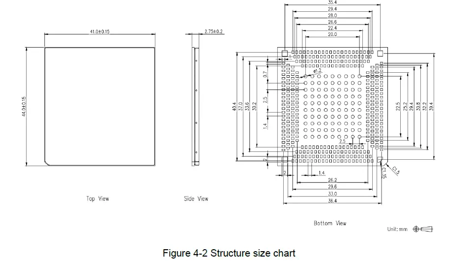
Note: Unmarked dimensional tolerances are 0.1mm.
Storage
Refer to the FIBOCOM FG360-NA Series SMT Design Guide.
Packing
Refer to the FIBOCOM FG360-NA Series SMT Design Guide.


