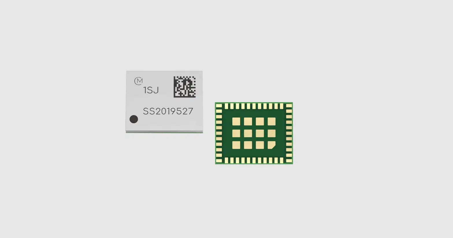
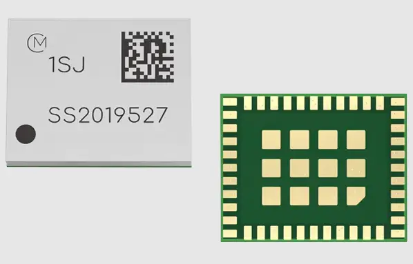
muRata 1SJ LoRa Module
Features
- Interfaces : UART, I2C, USB, SPI
- Main ICs : STM32L, SX1262
- Reference Clocks : Integrated 32MHz clock (TCXO with frequency error=±3.0
- ppm) and 32.768KHz clock (frequency error=±20 ppm)
Transmitting Channel Frequency Allocation:
- 125KHz LoRa: 902.3~914.9MHz, channel space 200KHz
- 500KHz LoRa: 903.0~914.2MHz, channel space 1.6MHz
- Module Size : 10.0 mm x 8.0 mm x 1.60 max mm.
- Weight : 0.28g (Typ.)
- Package : Resin mold
- RoHS : This module is compliant with the RoHS directive
Part Number
| Ordering Part Number | Description |
| LBAA0QB1SJ-295TEMP | Engineering sample |
| LBAA0QB1SJ-295EVK | Evaluation board |
| 1SJ | MP P/N |
Block Diagram
Confidential. Please contact Murata for the block diagram.
Certification info
4.1. Radio Certification
USA/Canada
| FCC ID | VPYLBAA0QB1SJ |
| IC | 772C-LBAA0QB1SJ |
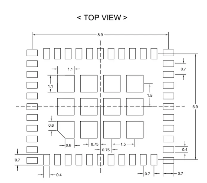
Dimensions, Marking and Terminal Configurations
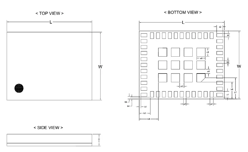
Table 1 Dimension (Unit: mm)
| Mark | Dimension | Mark | Dimension | Mark | Dimension |
| L | 10.0±0.2 | W | 8.0±0.2 | T | 1.60 max |
| a1 | 0.4±0.1 | a2 | 0.4±0.1 | a3 | 1.0±0.1 |
| b1 | 0.2±0.15 | b2 | 1.3±0.15 | b3 | 2.3±0.15 |
| b4 | 0.2±0.15 | b5 | 0.3±0.15 | b6 | 2.0±0.15 |
| b7 | 2.5±0.15 | c1 | 0.7±0.1 | c2 | 0.7±0.1 |
| c3 | 1.0±0.1 | e1 | 0.3±0.1 | e2 | 0.3±0.1 |
| e3 | 0.5±0.1 | e4 | 0.5±0.1 |
Terminal Configurations
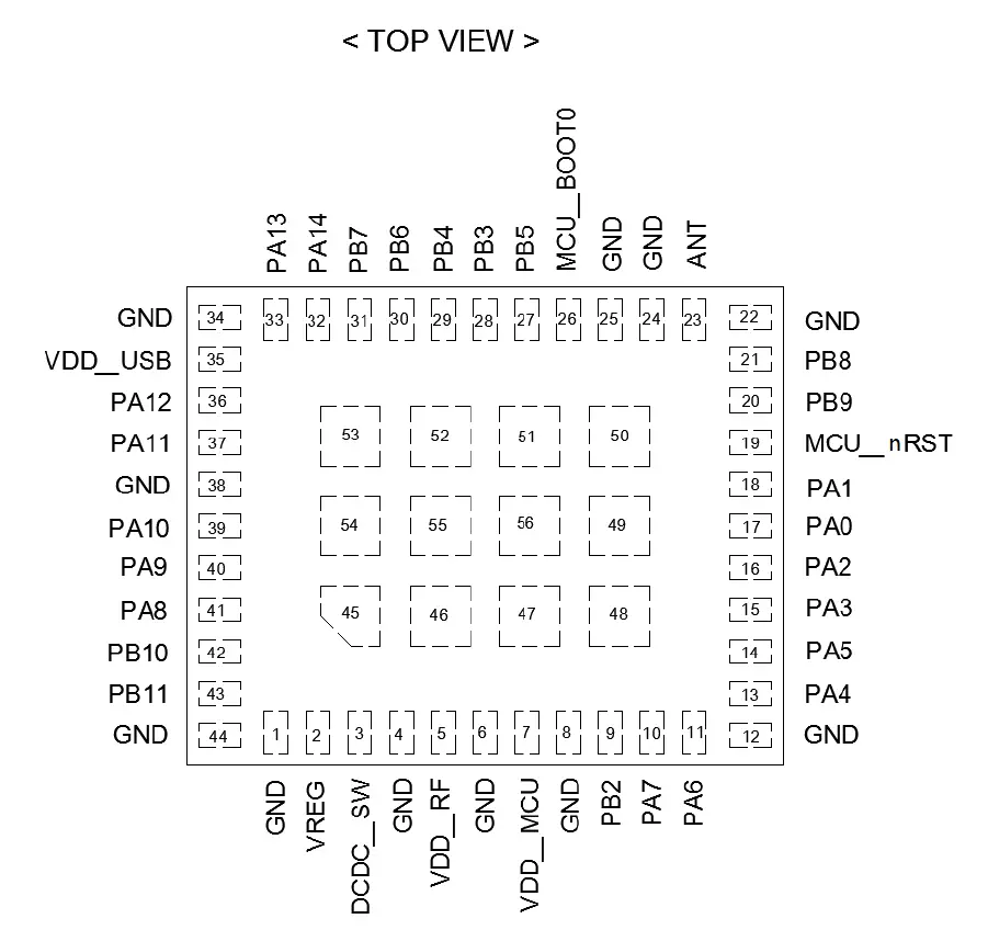
Table 2 Terminal Configurations
| Pin NO. | Terminal Name | Type | Connection to IC terminal | Description |
| 1 | GND | Ground | – | Ground |
| 2 | VREG | O | SX1262_VREG | Regulated output voltage from internal regulator LDO/DC-DC |
| 3 | DCDC_SW | O | SX1262_DCC_SW | DC-DC Switcher Output |
| 4 | GND | Ground | – | Ground |
| 5 | VDD_RF | Power | SX1262_VBAT / VDD_IN | Power supply for RF IC |
| 6 | GND | Ground | – | Ground |
| 7 | VDD_MCU | Power | SX1262_VBAT_IO,STM3 2L072_VDD / VDDA / VREF+ | Power supply for MCU and RF IC |
| 8 | GND | Ground | – | Ground |
| 9 | PB2 | I/O | STM32L072_PB2 | GPIO mode:PB2 LPTIM1_OUT |
| I2C3_SMBA | ||||
|
10 |
PA7 |
I/O |
STM32L072_PA7 | GPIO mode:PA7 SPI1_MOSI COMP2_OUT ADC_IN7 |
|
11 |
PA6 |
I/O |
STM32L072_PA6 | GPIO mode:PA6 SPI1_MISO LPUART1_CTS COMP1_OUT ADC_IN6 |
| 12 | GND | Ground | – | Ground |
|
13 |
PA4 |
I/O |
STM32L072_PA4 | GPIO mode:PA4 SPI1_NSS UART2_CK COMP1_INM/COMP2_INM ADC_IN4 DAC_OUT1 |
|
14 |
PA5 |
I/O |
STM32L072_PA5 | GPIO mode:PA5 SPI1_SCK CMP2_INM COMP1_INM/COMP2_INM ADC_IN5 DAC_OUT2 |
|
15 |
PA3 |
I/O |
STM32L072_PA3 | GPIO mode:PA3 ADC_IN3 USART2_RX LPUART1_RX COMP2_INP |
|
16 |
PA2 |
I/O |
STM32L072_PA2 | GPIO mode:PA2 ADC_IN2 USART2_TX LPUART1_TX COMP2_OUT/COMP2_INM |
|
17 |
PA0 |
I/O |
STM32L072_PA0 | GPIO mode:PA0 ADC_IN0 USART2_CTS USART4_TX COMP1_OUT/COMP1_INM |
|
18 |
PA1 |
I/O |
STM32L072_PA1 | GPIO mode:PA1 ADC_IN1 USART2_RTS USART4_RX COMP1_INP |
| 19 | MCU_nRST | I | STM32L072_nRST | Reset for MCU |
|
20 |
PB9 |
I/O |
STM32L072_PB9 | GPIO mode: PB9 I2C1_SDA SPI2_NSS I2S2_WS |
| 21 | PB8 | I/O | STM32L072_PB8 | GPIO mode:PB8 I2C1_SCL |
| 22 | GND | Ground | – | Ground |
| 23 | ANT | A, I/O | – | Transmit / Receive antenna |
| 24 | GND | Ground | – | Ground |
| 25 | GND | Ground | – | Ground |
| 26 | MCU_BOOT0 | I | STM32L072_BOOT0 | BOOT0 for MCU |
|
27 |
PB5 |
I/O |
STM32L072_PB5 | GPIO mode:PB5 LPTIM1_IN1 SPI1_MOSI I2C1_SMBA USART1_CK USART5_RTS COMP2_INP |
|
28 |
PB3 |
I/O |
STM32L072_PB3 | GPIO mode:PB3 COMP2_INM SPI1_CLK USART1_RTS USART5_TX |
|
29 |
PB4 |
I/O |
STM32L072_PB4 | GPIO mode:PB4 COMP2_INP SPI1_MISO USART1_CTS USART5_RX I2C3_SDA |
|
30 |
PB6 |
I/O |
STM32L072_PB6 | GPIO mode:PB6 I2C1_SCL USART1_TX LPTIM1_ETR COMP2_INP |
|
31 |
PB7 |
I/O |
STM32L072_PB7 | GPIO mode:PB7 I2C1_SDA USART1_RX LPTIM1_IN2 USART4_CTS COMP2_INP VREF_PVD_IN |
|
32 |
PA14 |
I/O |
STM32L072_PA14 | GPIO mode:PA14 SWCLK USART2_TX LPUART1_TX |
|
33 |
PA13 |
I/O |
STM32L072_PA13 | GPIO mode:PA13 SWDIO USB_OE LPUART1_RX |
| 34 | GND | Ground | – | Ground |
| 35 | VDD_USB | Power | STM32L072_VDD_USB | Power supply for MCU USB Interface |
|
36 |
PA12 |
I/O |
STM32L072_PA12 | GPIO mode:PA12(power supply by VDD_USB) USB_DP SPI1_MOSI USART1_RTS COMP2_OUT |
| 37 | PA11 | I/O | STM32L072_PA11 | GPIO mode:PA11(power supply by VDD_USB) |
| USB_DM SPI1_MISO USART1_CST COMP1_OUT | ||||
| 38 | GND | Ground | – | Ground |
| 39 | PA10 | I/O | STM32L072_PA10 | GPIO mode:PA10 USART1_RX I2C1_SDA |
|
40 |
PA9 |
I/O |
STM32L072_PA9 | GPIO mode:PA9 USART1_TX I2C1_SCL I2C3_SMBA MCO |
|
41 |
PA8 |
I/O |
STM32L072_PA8 | GPIO mode:PA8 MCO USB_CRS_SYNC USART1_CK I2C3_SCL |
|
42 |
PB10 |
I/O |
STM32L072_PB10 | GPIO mode:PB10 LPUART1_TX/LPUART1_RX SPI2_SCK I2C2_SCL |
| 43 | PB11 | I/O | STM32L072_PB11 | GPIO mode:PB11 LPUART1_RX/ LPUART1_TX I2C2_SDA |
| 44 | GND | Ground | – | Ground |
| 45~56 | GND | Ground | – | Ground |
Notes: GPIO pins are to be left OPEN if not used.
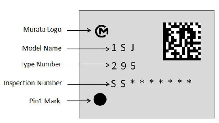
Label Information
Absolute Maximum Ratings
Table 3 Maximum ratings
| Parameters | Min | Typ | Max | Unit | |
| Storage Temperature | -40 | 25 | +85 | degC | |
| Input RF Level | – | – | 10 | dBm | |
| Supply Voltage | VDD_RF, VDD_MCU, VDD_USB | -0.3 | – | 3.9 | V |
Operating Condition
Table 4 Operating specification
| Parameters | Min | Typ | Max | Unit | |
| Operating Temperature | -40 | 25 | +85 | degC | |
| Supply Voltage | VDD_RF, VDD_MCU | 2.0 | – | 3.6 | V |
| VDD_USB (USB peripheral used) (1) | 3.0 | – | 3.6 | V | |
| VDD_USB(USB peripheral not used) (1) | VDD_MCU_min | VDD_MCU | VDD_MCU_max | V | |
VDD_USB must respect the following conditions:
- When VDD_MCU is powered on (VDD_MCU < VDD_MCU_min), VDD_USB should be always lower than VDD_MCU.
- When VDD_MCU is powered down (VDD_MCU < VDD_MCU_min), VDD_USB should be always lower than
- VDD_MCU.
- In operating mode, VDD_USB could be lower or higher than VDD_MCU.
- If the USB is not used, VDD_USB must be tied to VDD_MCU to be able to use PA11 and PA12 as standard I/O.
Electrical Characteristics
FSK Transceiver Specification
Conditions:
Supply voltage =3.3 V, Temperature = 25 °C, TCXO = 32 MHz, FRF =868MHz, all RF impedances matched, transmit mode output power defined in 50 Ohm load, FSK BER = 0.1%, 2-level FSK modulation without pre-filtering, BR = 4.8 kb/s, FDA = 5 kHz, BW_F = 19.5 kHz double-sided, unless otherwise specified.
Note: FSK transmission is only available in the EU868 band.
FSK Receive Specification
| Symbol | Description | Conditions | Min | Typ | Max | Unit |
| RXS_2FB | Sensitivity 2-FSK, RX Boosted, Split RF path for RX and TX | BR_F = 4.8 kb/s, FDA = 5 kHz, BW_F = 19.5 kHz | -117 | dBm |
FSK Transmit Specification
| Symbol | Description | Conditions | Min | Typ | Max | Unit |
| TXOP | Power setting = 22 dBm | 868MHZ Band | 21.5 | dBm | ||
| IDDTX | Power setting = 22 dBm | 868MHZ Band | 118 | mA |
LoRa Transceiver Specification
Conditions:
The table below gives the electrical specifications for the transceiver operating with LoRaTM modulation. Following conditions apply unless otherwise specified: Supply voltage = 3.3 V, Temperature = 25 °C, TCXO = 32 MHz, FRF =868/915 MHz, all RF impedances matched, transmit mode output power defined in 50 Ohm load, Error Correction Code (EC) = 4/5, Packet Error Rate (PER)= 1%, CRC on payload enabled, Payload length = 10 bytes.
LoRa Receive Specification
| Symbol | Description | Conditions | Min | Typ | Max | Unit |
| IDDRX | Receive mode, DC-DC mode used, RX Boosted, | 868MHZ Band | 15.5(1) | mA | ||
| 915MHz Band | 15.5(1) | mA | ||||
| IDDRX | Receive mode, LDO mode used, RX Boosted | 868MHZ Band | 20.0(1) | mA | ||
| 915MHz Band | 20.0(1) | mA | ||||
| RXS_LB (125KHz) | Sensitivity Lora, RX Boosted, Split RF path for RX and TX. 125KHz bandwidth | SF = 7 | -124 | dBm | ||
| SF = 12 | -137 | dBm | ||||
| RXS_LB (250KHz) | Sensitivity Lora, RX Boosted, Split RF path for RX and TX. 250KHz bandwidth | SF = 7 | -121 | dBm | ||
| SF = 12 | -134 | dBm |
(1) IDDRX is tested under test FW, and MCU is not in sleep mode.
LoRa Transmit Specification
| Symbol | Description | Conditions | Min | Typ | Max | Unit |
| TXOP | TXOP setting = 22 dBm | 868MHZ Band | 22 | dBm | ||
| 915MHZ Band | 22 | dBm | ||||
| IDDTX | TXOP setting = 22 dBm | 868MHZ Band | 118 | mA | ||
| 915MHZ Band | 109 | mA |
Low power mode current
Conditions: Power supply=3.3 V, Temperature=25 °C;
| Description | Min | Typ | Max | Unit |
| STM32L072 in stop mode with RTC (Real Time Clock) SX1262 in cold start sleep mode1 | 1.3 | uA | ||
| STM32L072 in stop mode with RTC (Real Time Clock) SX1262 in warm start sleep mode without RC64K(64kHz RC oscillator)2 | 2.0 | uA | ||
| STM32L072 in stop mode with RTC (Real Time Clock) SX1262 in warm start sleep mode with RC64K(64kHz RC oscillator)2 | 2.5 | uA |
- Cold start is equivalent to device at POR or when the device is waking up from sleep mode with all blocks OFF.
- Warm start is only happening when device is waking up from sleep mode with its configuration retained.
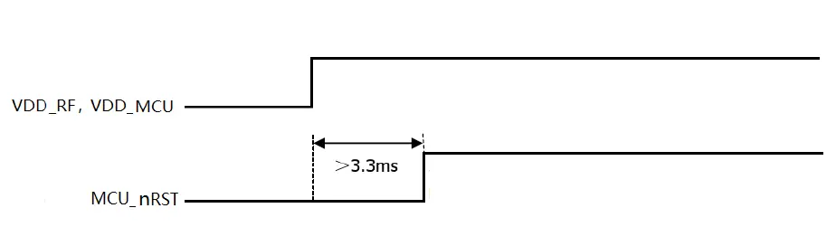
10. Power Sequences
Power Up Sequence
Recommend Land Pattern
Notes:
- Dimension unit is millimeter (Angle unit is degree).
- This land pattern is for reference only. Consult your manufacturing group to ensure your company’s manufacturing guidelines are met.
- Thermal vias in the land pattern of the exposed pad shall be connected to a system ground plane. Failure to do so may compromise the thermal and/or functional performance of the device.
- Square package-dimension apply in both “X” and “Y” directions.
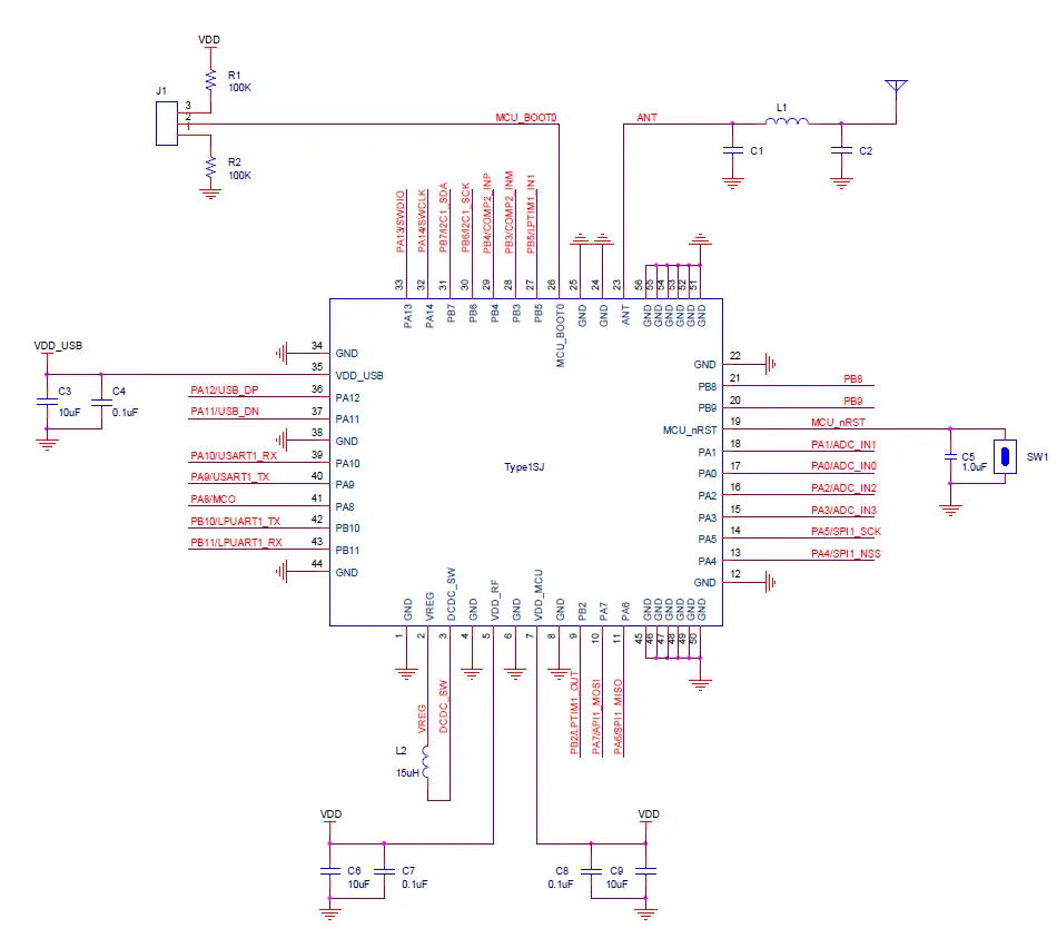
Reference Circuit
Tape and Reel Packing
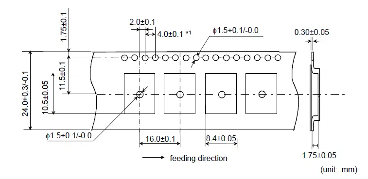
Dimension of Tape
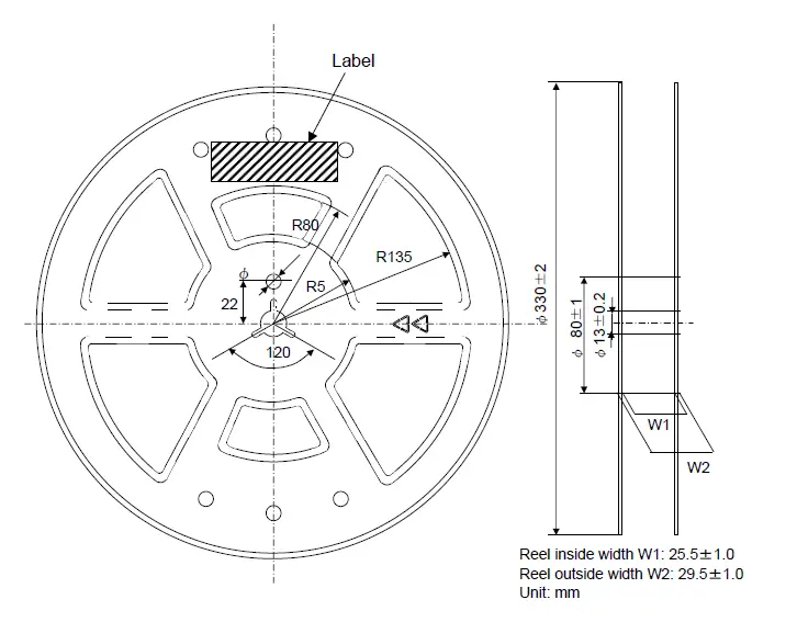
Dimensions of Reel
Taping Diagrams
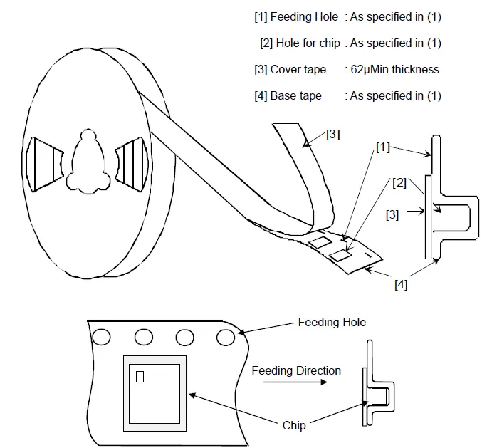
Leader and Tail Tape 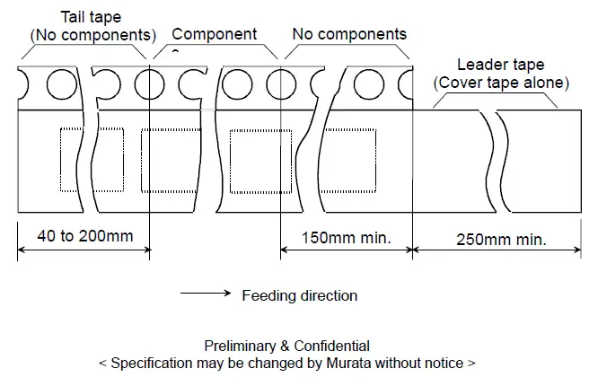
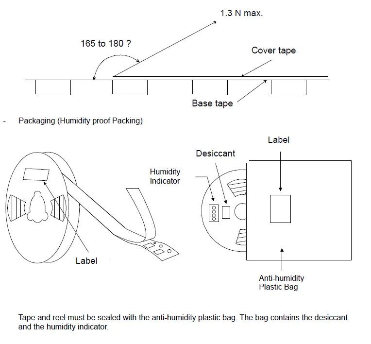
- The tape for chips are wound clockwise, the feeding holes to the right side as the tape is pulled toward the user.
- The cover tape and base tape are not adhered at no components area for 250mm Min.
- Tear off strength against pulling of cover tape: 5N Min.
- Packaging unit : 1000 pcs/ reel
- Material
- Base tape : Plastic
- Reel : Plastic
- Cover tape, cavity tape and reel are made the anti-static processing.
- Peeling of force: 1.3N max. in the direction of peeling as shown below.
Notice
Storage Conditions
Please use this product within 6month after receipt.
- The product shall be stored without opening the packing under the ambient temperature from 5 to 35 °C and humidity from 20 ~ 70 %RH. (Packing materials, in particular, may be deformed at the temperature over 40 °C)
- The product left more than 6months after reception, it needs to be confirmed the solderbility before used.
- The product shall be stored in non-corrosive gas (CL2, NH3, SO2, NOx, etc.).
- Any excess mechanical shock including, but not limited to, sticking the packing materials by sharp object and dropping the product, shall not be applied in order not to damage the packing materials.
This product is applicable to MSL3 (Based on IPC/JEDEC J-STD-020)
- After the packing opened, the product shall be stored at <30 °C / <60 %RH and the product shall be used within 168 hours.
- When the color of the indicator in the packing changed, the product shall be baked before soldering.
Baking condition: 125 +5/-0 °C, 24 hours, 1 time
The products shall be baked on the heat-resistant tray because the material (Base Tape, Reel Tape and Cover Tape) are not heat-resistant.
Handling Conditions
Be careful in handling or transporting products because excessive stress or mechanical shock may break products.
Handle with care if products may have cracks or damages on their terminals, the characteristics of products may change. Do not touch products with bear hands that may result in poor solderability.
Standard PCB Design (Land Pattern and Dimensions)
All the ground terminals should be connected to the ground patterns. Furthermore, the ground pattern should be provided between IN and OUT terminals. Please refer to the specifications for the standard land dimensions.
The recommended land pattern and dimensions is as Murata’s standard. The characteristics of products may vary depending on the pattern drawing method, grounding method, land dimensions, land forming method of the NC terminals and the PCB material and thickness. Therefore, be sure to verify the characteristics in the actual set. When using non-standard lands, contact Murata beforehand.
Notice for Chip Placer :
When placing products on the PCB, products may be stressed and broken by uneven forces from a worn-out chucking locating claw or a suction nozzle. To prevent products from damages, be sure to follow the specifications for the maintenance of the chip placer being used. For the positioning of products on the PCB, be aware that mechanical chucking may damage products.
Soldering Conditions:
The recommendation conditions of soldering are as in the following figure.
When products are immersed in solvent after mounting, pay special attention to maintain the temperature difference within 100 °C. Soldering must be carried out by the above mentioned conditions to prevent products from damage. Set up the highest temperature of reflow within 260 °C.
Contact Murata before use if concerning other soldering conditions.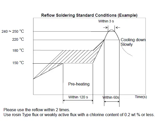
Please use the reflow within 2 times.
Use rosin Type flux or weakly active flux with a chlorine content of 0.2 wt % or less.
Cleaning :
Since this Product is Moisture Sensitive, any cleaning is not permitted.
Operational Environment Conditions :
Products are designed to work for electronic products under normal environmental conditions (ambient temperature, humidity and pressure). Therefore, products have no problems to be used under the similar conditions to the above-mentioned. However, if products are used under the following circumstances, it may damage products and leakage of electricity and abnormal temperature may occur.
- In an atmosphere containing corrosive gas (CL2, NH3, SOx, NOx, etc.).
- In an atmosphere containing combustible and volatile gases.
- Dusty place.
- Direct sunlight place.
- Water splashing place.
- Humid place where water condenses.
- Freezing place.
If there are possibilities for products to be used under the preceding clause, consult with Murata before actual use.
As it might be a cause of degradation or destruction to apply static electricity to products, do not apply static electricity or excessive voltage while assembling and measuring.
14.8. Input Power Capacity :
Products shall be used in the input power capacity as specified in this specification.
Inform Murata beforehand, in case that the components are used beyond such input power capacity range.
Regulatory Statements
FCC Statements
This product has been tested and found to comply with the limits for a Class B digital device, pursuant to Part 15 of the FCC Rules. These limits are designed to provide reasonable protection against harmful interference in a residential installation. This product generates, uses, and can radiate radio frequency energy and, if not installed and used in accordance with the instructions, may cause harmful interference to radio communications. However, there is no guarantee that interference will not occur in a particular installation. If this product does cause harmful interference to radio or television reception, which can be determined by turning the equipment off and on, the user is encouraged to try to correct the interference by one or more of the following measures:
- Reorient or relocate the receiving antenna.
- Increase the separation between the equipment and receiver.
- Connect the equipment into an outlet on a circuit different from that to which the receiver is connected.
- Consult the dealer or an experienced radio/TV technician for help.
This equipment should be installed and operated with a minimum distance 20cm between the radiator and your body
Please take attention that changes or modification not expressly approved by the party responsible for compliance could void the user’s authority to operate the equipment.
IC Statements
This device complies with Industry Canada licence-exempt RSS standard(s). Operation is subject to the following two conditions:
- this device may not cause interference, and
- this device must accept any interference, including interference that may cause undesired operation of the device.
Under Industry Canada regulations, this radio transmitter may only operate using an antenna of a type and maximum (or lesser) gain approved for the transmitter by Industry Canada. To reduce potential radio interference to other users, the antenna type and its gain should be so chosen that the equivalent isotropically radiated power (e.i.r.p.) is not more than that necessary for successful communication.
This equipment should be installed and operated with a minimum distance 20cm between the radiator and your body
When the Industry Canada certification number is not visible when the module is installed inside another device, then the outside of the device into which the module is installed must also display a label referring to the enclosed module. This exterior label can be use wording ”Contains transmitter module IC: 772C-LBAA0QB1SJ”or “Contains IC: 772C-LBAA0QB1SJ”.
General Statements
The module is limited to OEM installation ONLY.
The OEM integrator is responsible for ensuring that the end-user has no manual instruction to remove or install module.
Therefore, the final host product must be submitted to Murata for confirmation that the installation for the module into the host is in compliance with regulations of FCC and IC Canada. Specially, if an antenna other than the model documented in the Filing is used, a Class 2 Permissive Change must be filed with the FCC.
Changes or modifications not expressly approved by the manufacturer could void the user’s authority to operate the equipment.
The LoRa module is for use with external antenna ONLY.
The certified antennas include:
- PCB pattern Antenna with peak gain 1.0dBi.
- Flexible Antenna (Molex: 2111400100) with peak gain 1.0dBi.
- Chip Antenna NN02-224 with peak gain 0.9dBi.
This module has been approved by FCC to operate with the antenna types with the maximum permissible gain indicated. Antenna types not included in this list, having a gain greater than the maximum gain indicated for that type, are strictly prohibited for use with this device.
CAUTION
PLEASE READ THIS NOTICE BEFORE USING OUR PRODUCTS.
Please make sure that your product has been evaluated and confirmed from the aspect of the fitness for the specifications of our product when our product is mounted to your product.
All the items and parameters in this product specification/datasheet/catalog have been prescribed on the premise that our product is used for the purpose, under the condition and in the environment specified in this specification. You are requested not to use our product deviating from the condition and the environment specified in this specification.
Please note that the only warranty that we provide regarding the products is its conformance to the specifications provided herein. Accordingly, we shall not be responsible for any defects in products or equipment incorporating such products, which are caused under the conditions other than those specified in this specification.
WE HEREBY DISCLAIMS ALL OTHER WARRANTIES REGARDING THE PRODUCTS, EXPRESS OR IMPLIED, INCLUDING WITHOUT LIMITATION ANY WARRANTY OF FITNESS FOR A PARTICULAR PURPOSE, THAT THEY ARE DEFECT-FREE, OR AGAINST INFRINGEMENT OF INTELLECTUAL PROPERTY RIGHTS.
The product shall not be used in any application listed below which requires especially high reliability for the prevention of such defect as may directly cause damage to the third party’s life, body or property. You acknowledge and agree that, if you use our products in such applications, we will not be responsible for any failure to meet such requirements.
Furthermore, YOU AGREE TO INDEMNIFY AND DEFEND US AND OUR AFFILIATES AGAINST ALL CLAIMS, DAMAGES, COSTS, AND EXPENSES THAT MAY BE INCURRED, INCLUDING WITHOUT LIMITATION, ATTORNEY FEES AND COSTS, DUE TO THE USE OF OUR PRODUCTS IN SUCH APPLICATIONS.
- Aircraft equipment.
- Aerospace equipment
- Undersea equipment.
- Power plant control equipment
- Medical equipment.
- Transportation equipment (vehicles, trains, ships, elevator, etc.).
- Traffic signal equipment.
- Disaster prevention / crime prevention equipment.
- Burning / explosion control equipment
- Application of similar complexity and/ or reliability requirements to the applications listed in the above.
We expressly prohibit you from analyzing, breaking, Reverse-Engineering, remodeling altering, and reproducing our product. Our product cannot be used for the product which is prohibited from being manufactured, used, and sold by the regulations and laws in the world.
We do not warrant or represent that any license, either express or implied, is granted under any our patent right, copyright, mask work right, or our other intellectual property right relating to any combination, machine, or process in which our products or services are used. Information provided by us regarding third-party products or services does not constitute a license from us to use such products or services or a warranty or endorsement thereof. Use of such information may require a license from a third party under the patents or other intellectual property of the third party, or a license from us under our patents or other intellectual property.
Please do not use our products, our technical information and other data provided by us for the purpose of developing of mass-destruction weapons and the purpose of military use.
Moreover, you must comply with “foreign exchange and foreign trade law”, the “U.S. export administration regulations”, etc.
Please note that we may discontinue the manufacture of our products, due to reasons such as end of supply of materials and/or components from our suppliers.
Customer acknowledges that Murata will, if requested by you, conduct a failure analysis for defect or alleged defect of Products only at the level required for consumer grade Products, and thus such analysis may not always be available or be in accordance with your request (for example, in cases where the defect was caused by components in Products supplied to Murata from a third party).
By signing on specification sheet or approval sheet, you acknowledge that you are the legal representative for your company and that you understand and accept the validity of the contents herein. When you are not able to return the signed version of specification sheet or approval sheet within 90 days from receiving date of specification sheet or approval sheet, it shall be deemed to be your consent on the content of specification sheet or approval sheet.
Customer acknowledges that engineering samples may deviate from specifications and may contain defects due to their development status.
We reject any liability or product warranty for engineering samples. In particular we disclaim liability for damages caused by
- the use of the engineering sample other than for evaluation purposes, particularly the installation or integration in the product to be sold by you,
- deviation or lapse in function of engineering sample,
- improper use of engineering samples.
We disclaim any liability for consequential and incidental damages.
If you can’t agree the above contents, you should inquire our sales.


