
Microsemi UG0640 Bayer Interpolation
Revision History
The revision history describes the changes that were implemented in the document. The changes are listed by revision, starting with the most current publication.
Revision 5.0
The following is a summary of changes in this revision.
- Updated Introduction, page 2.
- Updated Figure 1, page 2, Figure 2, page 4, Figure 3, page 6, and Figure 4, page 6.
- Updated tables such Interfaces, page 5.
- Updated Resource Utilization, page 13.
- Updated Test Bench, page 7.
- Updated Simulation Results, page 12.
Revision 4.0
Updated the resource Utilization.
Revision 3.0
Updated the testbench information.
Revision 2.0
The following is a summary of the changes in this revision.
- Added the TestBench section.
Revision 1.0
The first publication of this document
Introduction
Bayer Interpolation coverts an image in Bayer color filter array format to RGB per pixel format. The following figure shows the demos icing of a Bayer format image.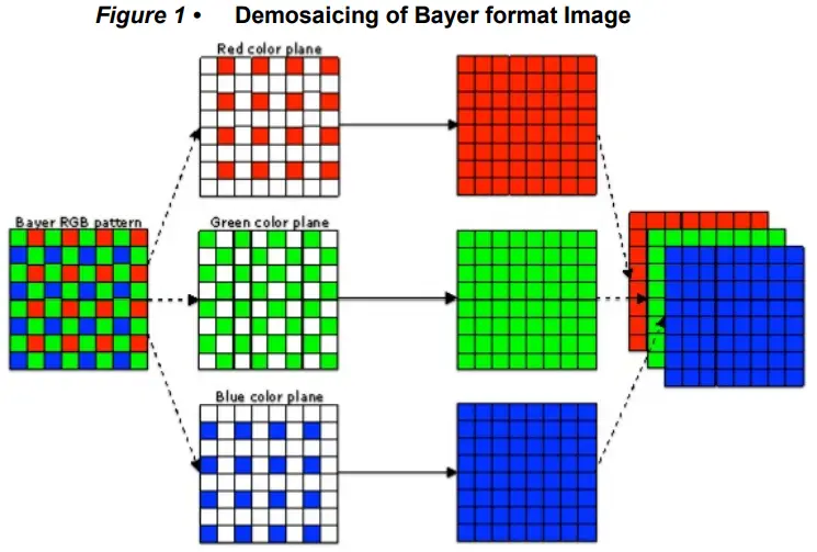
There are several standard interpolation methods. The simplest interpolation method is bilinear interpolation. The Bayer interpolation IP uses the bilinear interpolation methods to covert a Bayer format image to RGB format.
Bilinear Interpolation
The bilinear algorithm processes each pixel separately and finds out the missing components in it by applying linear interpolation to the available ones.
The formulas for calculating missing component at a particular pixel by considering 3×3 window are as follows.
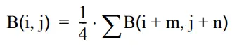
Green component at red and blue pixel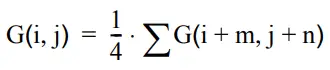
where (m,n) = {(0,-1)(0,1)(-1,0)(1,0)}
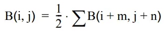
Red component at blue pixel
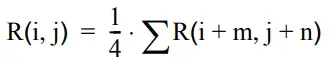
where (i,j) = {(-1,-1)(-1,1)(1,-1)(1,1)}
Red component at green pixel
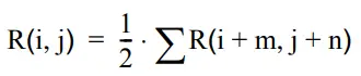
where (m,n) = {(0,-1)(0,1)} or (m,n) = {(-1,0)(1,0)}
Blue component at red pixel
where (m,n) = {(-1,-1)(-1,1)(1,-1)(1,1)}
Blue component at green pixel
where (m,n) = {(0,-1)(0,1)} or (m,n) = {(-1,0)(1,0)}
Hardware Implementation
The following figure shows the block diagram of Bayer interpolation.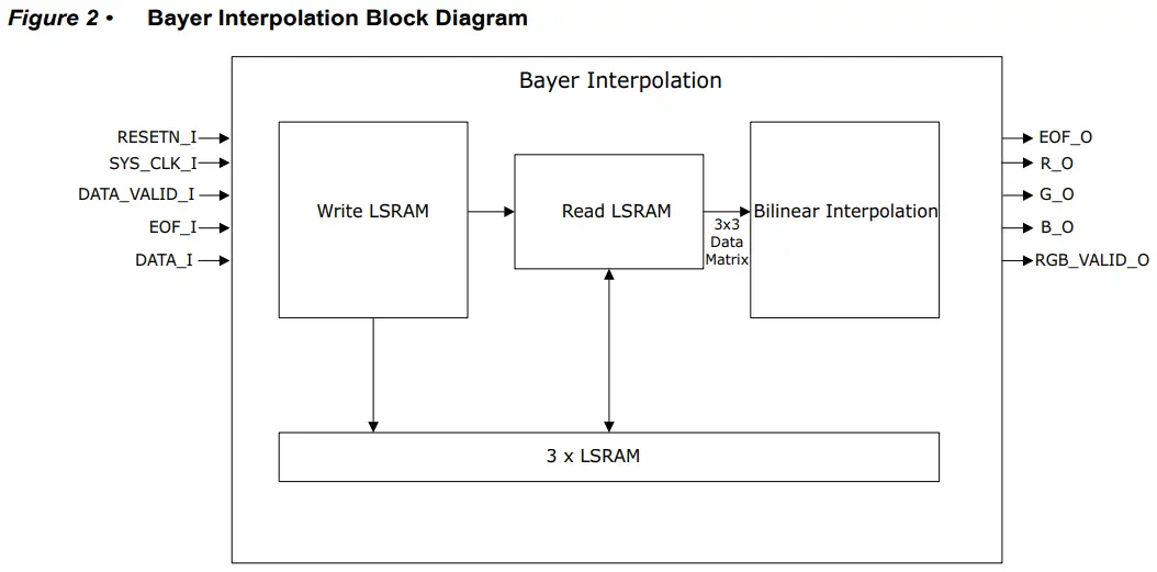
The Bayer interpolation IP consists of the following three submodules.
- Write LSRAM, page 4
- Read LSRAM, page 4
- Bilinear Interpolation, page 4
Write LSRAM
The raw image data coming from camera sensor is written into 3 different LSRAM. The 1st, 4th, 7th …… line of the frame are written to LSRAM1, the 2nd, 5th, 8th …… line of the frame are written into LSRAM2 and the 3rd, 6th, 9th ….. line of the frame are written into LSRAM3. The LSRAM addresses and write enable signals are generated by write LSRAM submodule.
Read LSRAM
The read submodule generates the read enable signals and the addresses to read from LSRAM. It also has the 3×3 window logic which reads the 3×3 window from LSRAMs and feeds to the bilinear interpolation block. The pixel at which the color components are to be computed is placed at the center of the 3×3 window. Then the window slides right to compute the value of the next pixel in the line.
For the first line of the frame, the first row of the 3×3 window is all zeros, the second row is LSRAM1 data and third row is LSRAM2 data. For the second line, the first row is LSRAM1 data, second row is LSRAM2 data and third row is LSRAM3 data. For the third line, the first row is LSRAM2 data, second row is LSRAM3 data and third row is LSRAM1 data and so on.
Bilinear Interpolation
The bilinear interpolation module computes the R, G and B value for the center element of the 3×3 data matrix coming from read LSRAM module. It computes the R, G and B value based on the bilinear interpolation formulae described in Bilinear Interpolation, page 2.
The Bayer interpolation IP automatically detects the video resolution. The IP uses the data from first frame to compute the horizontal and vertical resolution. As a result, the IP does not generate output (data valid is zero) during the first frame.
Interfaces
This section describes the input/output ports and configuration parameters of the Bayer Interpolation IP.
Ports
The following figure shows the input and output ports of Bayer interpolation.
Table 1 ï Input and Output Ports
| Port Name | Type | Width | Description |
| RESETN_I | Input | 1bit | Active low asynchronous reset signal to design |
| SYS_CLK_I | Input | 1bit | System clock |
| DATA_VALID_I | Input | 1bit | Asserted high when input data is valid |
| EOF_I | Input | 1bit | End of frame input signal |
| DATA_I | Input | G_DATA_WIDTH bits | Bayer data input |
| RGB_VALID_O | Output | 1bit | Asserted high when output data is valid |
| R_O | Output | G_DATA_WIDTH bits | Provides the red component output |
| G_O | Output | G_DATA_WIDTH bits | Provides the green component output |
| B_O | Output | G_DATA_WIDTH bits | Provides the blue component output |
| EOF_O | Output | 1bit | End of frame output. The first EOF_I is skipped and subsequent EOF_I inputs are passed through. |
Configuration Parameters
The following table shows the description of the configuration parameters used in the hardware implementation of Bayer Interpolation. These are generic parameters and can be varied as per the requirement of the application.
Table 2 ï Configuration Parameters
| Name | Descriptio |
| G_DATA_WIDTH | Width of each pixel |
| G_RAM_SIZE | Size of the RAM to store one horizontal line Choose values which are powers of 2, such as 2048, and 4096. |
| G_BAYER_FORMAT1 | Bayer format |
1. If G_BAYER_FORMAT = 0, then Bayer format is RGGB
If G_BAYER_FORMAT = 1, then Bayer format is GRBG
If G_BAYER_FORMAT = 2, then Bayer format is GBRG
If G_BAYER_FORMAT = 3, then Bayer format is BGGR
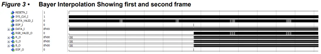
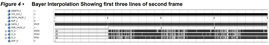
Timing Diagrams
The following figure shows the timing diagram of Bayer Interpolation.
Test Bench
Atestbench is provided to check the functionality of Bayer Interpolation IP. The following table shows the parameters that can be configured according to the application.
Table 3 ï Testbench Configuration Parameters
| Name | Description |
| CLKPERIOD | Clock Period |
| g_DATAWIDTH | Width of each pixel |
| g_DISPLAY_RESOLUTION | Horizontal resolution |
| g_VERT_DISPLAY_RESOLUTION | Vertical resolution |
| WAIT | Number of clock cycles delay between transmission of two input lines |
| IMAGE_FILE_NAME | Input (image) file name |
Simulation Steps
The following steps describe how to simulate the core using the testbench:
- On Libero SoC Design Flow, expand Create Design and open Create SmartDesign Testbench as shown in the following figure.

- Enter a name for the SmartDesign testbench and click OK as shown in Figure 6, page 8.
The SmartDesign testbench is created, and a canvas appears to the right of the Design Flow pane.
- Go to Libero SoC Catalog > View > Windows > Catalog, and then expand Solutions-Video.

- Drag and drop the Bayer IP core in to the new SmartDesign testbench canvas. The IP appears as shown in the following figure.

- Select all of the ports and promote them to top level as shown in the following figure.

- To generate the testbench component, select Generate Component from the SmartDesign toolbar, as highlighted in the following figure.

- Go to the Files tab and select simulation > Import Files as shown in the following figure.

- Import the CFA file from the following path:
..\\component\Microsemi\Solution Core\Bayer Conversion Top \3.0.0\Stimulus To import a different file, browse the folder that contains the required file, and click Open. The imported file is listed under simulation as shown in the following figure.
- Go to the Stimulus Hierarchy tab and select bayer-test (Bayer_interpolation_tb.v) > Simulate Pre-Synth Design > Open Interactively. The IP is simulated for one frame.

ModelSim opens with the testbench file as shown in Figure 14, page 10.
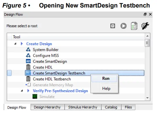
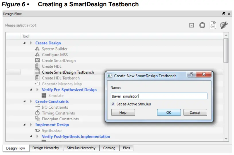
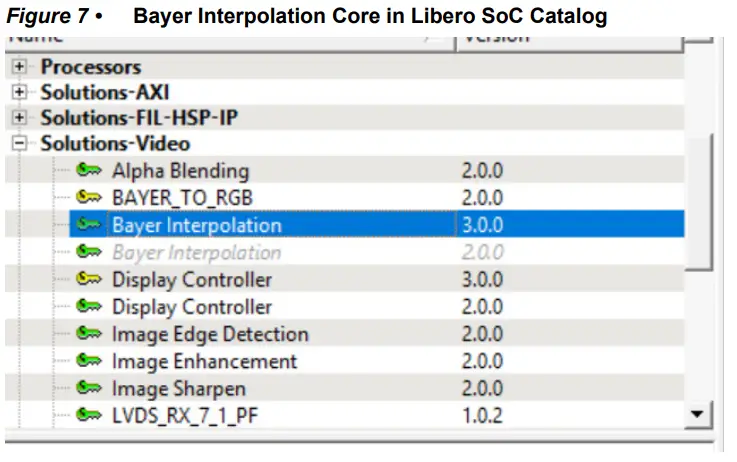
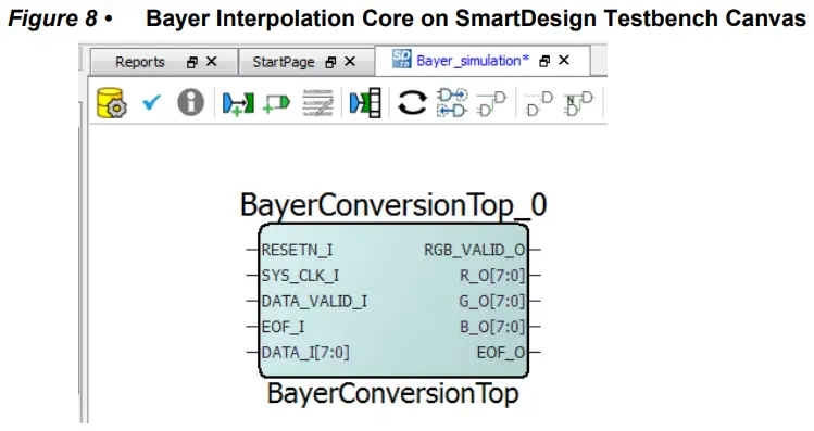
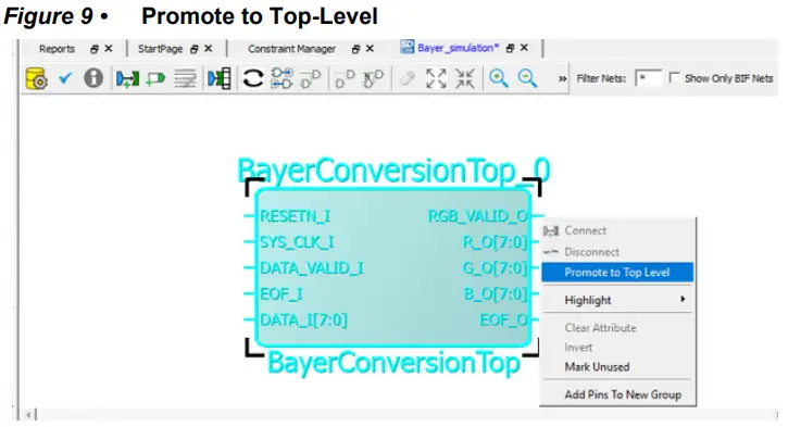
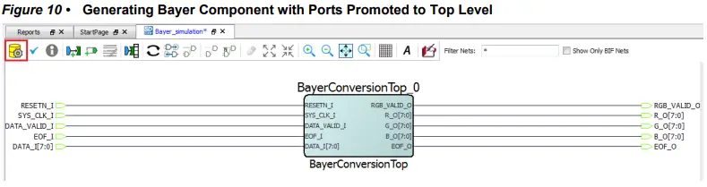
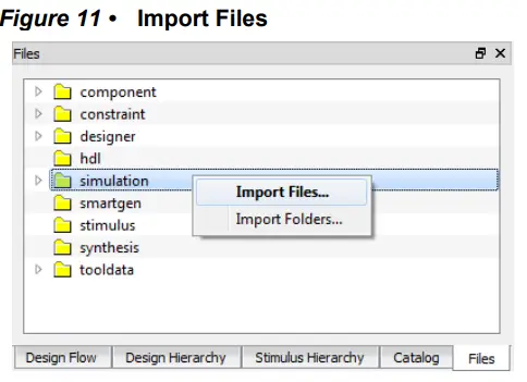
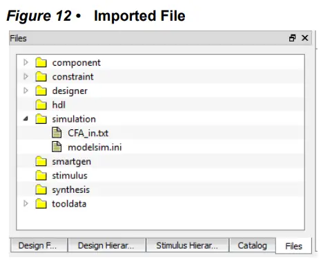
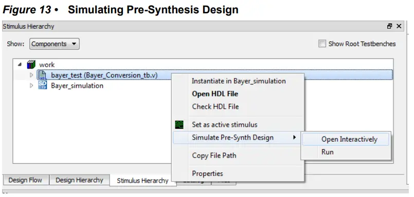
Figure 14 • ModelSim Simulation Window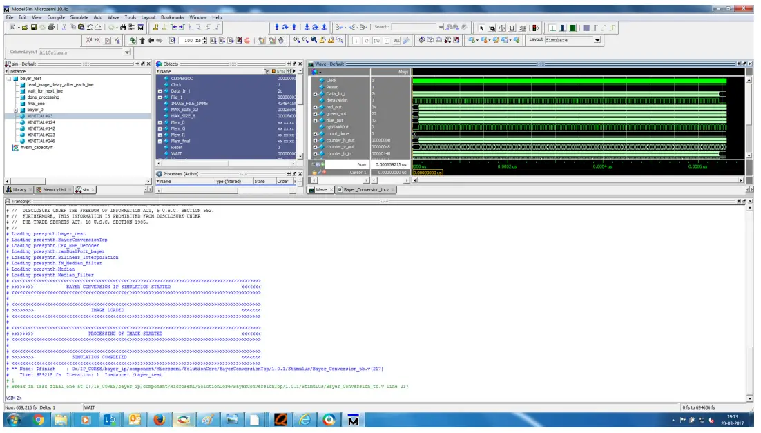
If the simulation is interrupted due to the runtime limit specified in the DO file, use the run -all command to complete the simulation.
The testbench output image file appears in the Files/simulation folder after the simulation completes.
Simulation Results
The following figure shows the input Bayer image.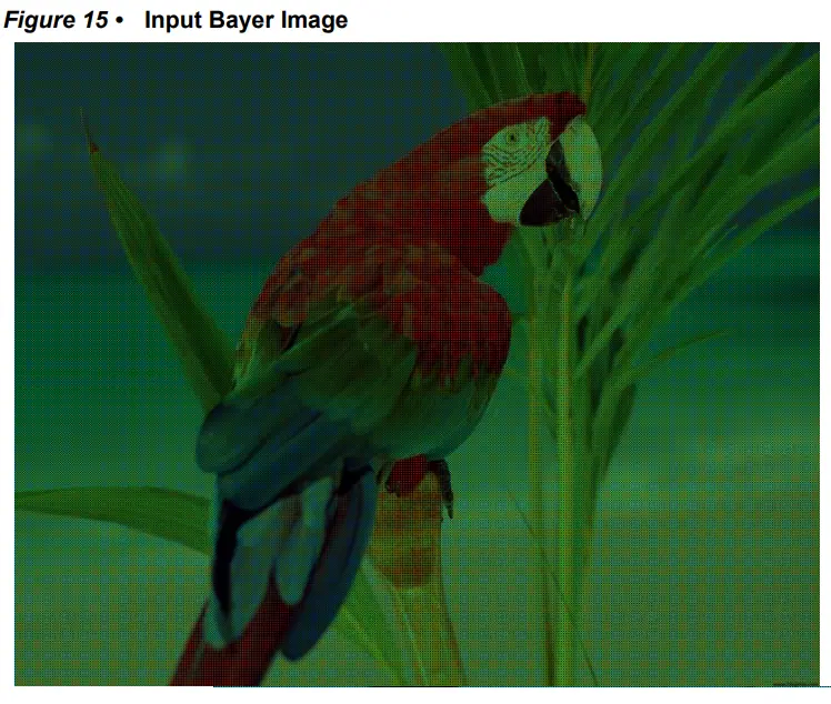
Output RGB Image
The following figure shows the output RGB image.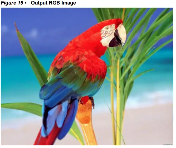
Resource Utilization
Bayer Interpolation is implemented on the SmartFusion®2 system-on-chip (SoC) field programmable gate array (FPGA) device (M2S150T-1152 FC package) and PolarFire® FPGA (MPF300TS – 1FCG1152E package). The following figure shows the resource utilization report after synthesis.
Table 4 Resource Utilization on PolarFire1
| Resource | Usage |
| DFFs | 550 |
| 4LUTs | 1020 |
| LSRAM | 3 |
| MACC | 0 |
- For G_DATA_WIDTH = 8, G_RAM_SIZE = 2048 and G_BAYER_FORMAT = 0.
Table 5 • Resource Utilization on SmartFusion21
| Resource | Usage |
| DFFs | 580 |
| 4LUTs | 1060 |
| RAM1K18 | 3 |
| RAM64x18 | 0 |
| MACC | 0 |
- for G_DATA_WIDTH = 8, G_RAM_SIZE = 2048 and G_BAYER_FORMAT = 0.


