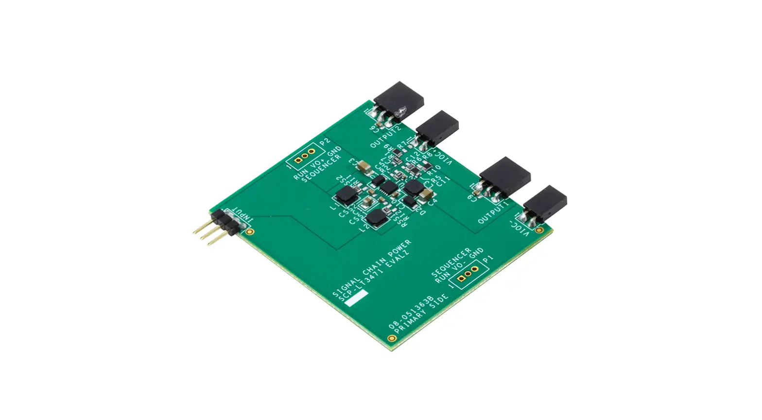
ANALOG DEVICES LT3471 Adaptable Voltage Drive Noise and Stability Optimized

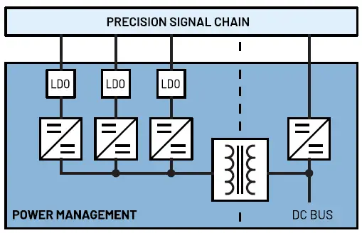
PRECISION SIGNAL CHAIN
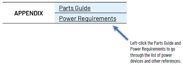
This document is interactive. You can click on any underlined text to navigate through the document.
For the resources

For the individual pages: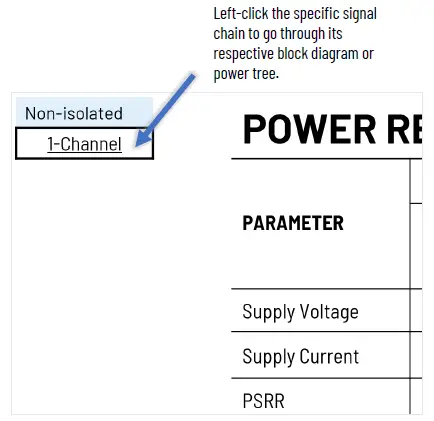
APPENDIX 1-Channel
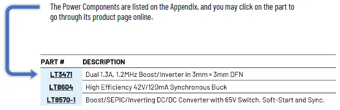
PART
| PART # | DESCRIPTION |
| LT3471 | Dual 1.3A, 1.2MHz Boost/Inverter in 3mm × 3mm DFN |
| LT8604 | High Efficiency 42V/120mA Synchronous Buck |
| LT8570 | Boost/SEPIC/Inverting DC/DC Converter with 65V Switch, Soft-Start and Sync. |
| LT3999 | Low Noise, 1A, 1MHz Push-Pull DC/DC Driver with Duty Cycle Control |
| ADP7118 | 20V, 200mA, Low Noise, CMOS LDO Linear Regulator |
| ADP7142 | 40V, 200 mA, Low Noise, CMOS LDO Linear Regulator |
| ADP7182 | –28V, −200mA, Low Noise, Linear Regulator |
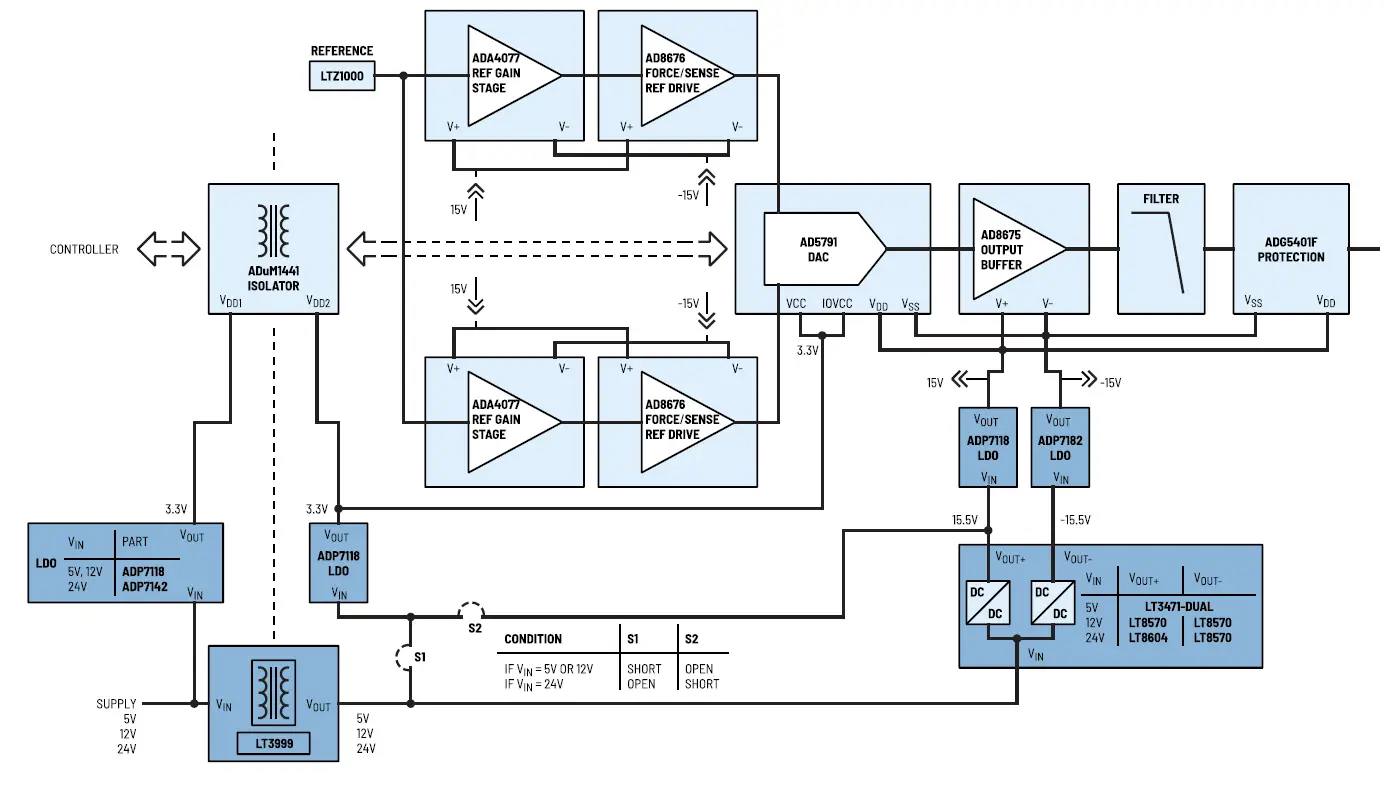
POWER REQUIREMENTS
| PARAMETER | STAGES | Buffer | Buffer | Isolation | DAC | Amp | Protection | ||||||||
| Part # | ADA4077 | AD8676 | ADuM1441 | AD5791 | AD8675 | ADG5401F | |||||||||
| Pin | V+ | V- | V+ | V- | VDD1 | VDD2 | VCC | IOVCC | VDD | VSS | V+ | V- | VDD | VSS | |
| Supply Voltage | V | 15 | -15 | 15 | -15 | 3.3 | 3.3 | 3.3 | 3.3 | 15 | -15 | 15 | -15 | 15 | -15 |
| Supply Current | mA | 0.65 | -0.65 | 4.2 | -4.2 | 0.9 | -0.75 | 0.9 | 0.14 | 5.2 | -4.9 | 3.8 | -3.8 | 0.22 | 0.09 |
| PSRR | dB | 12 (1MHz) | 24 (1MHz) | 22 (1MHz) | 68 (1MHz) | – | – | 48 (1MHz) | 52 (1MHz) | 82 (1MHz) | |||||
- Note 1: The supply currents indicated are the maximum quiescent current of the supply rails. For overall full load or short circuit current specifications, refer to the datasheets of the signal chain components.
- Note 2: The supply voltages indicated are the values for typical applications.
- Note 3: Consult the corresponding datasheets for details on power dissipation if needed.
- Note 4: The actual supply current requirement shall be multiplied depending on the number of channels on the signal chain.
References
 Mixed-signal and digital signal processing ICs | Analog Devices
-
ADP7118 Datasheet and Product Info | Analog Devices
-
ADP7142 Datasheet and Product Info | Analog Devices
-
ADP7182 Datasheet and Product Info | Analog Devices
-
AD5791 Datasheet and Product Info | Analog Devices
-
AD8675 Datasheet and Product Info | Analog Devices
-
AD8676 Datasheet and Product Info | Analog Devices
-
ADA4077-2 Datasheet and Product Info | Analog Devices
-
ADG5401F Datasheet and Product Info | Analog Devices
-
ADUM1441 Datasheet and Product Info | Analog Devices
-
LT3471 Datasheet and Product Info | Analog Devices
-
LT3999 Datasheet and Product Info | Analog Devices
-
LT8570 Datasheet and Product Info | Analog Devices
-
LT8604/LT8604C Datasheet and Product Info | Analog Devices


