
RAK2247 SPI WisLink-LoRa Concentrator Module
Overview
Introduction
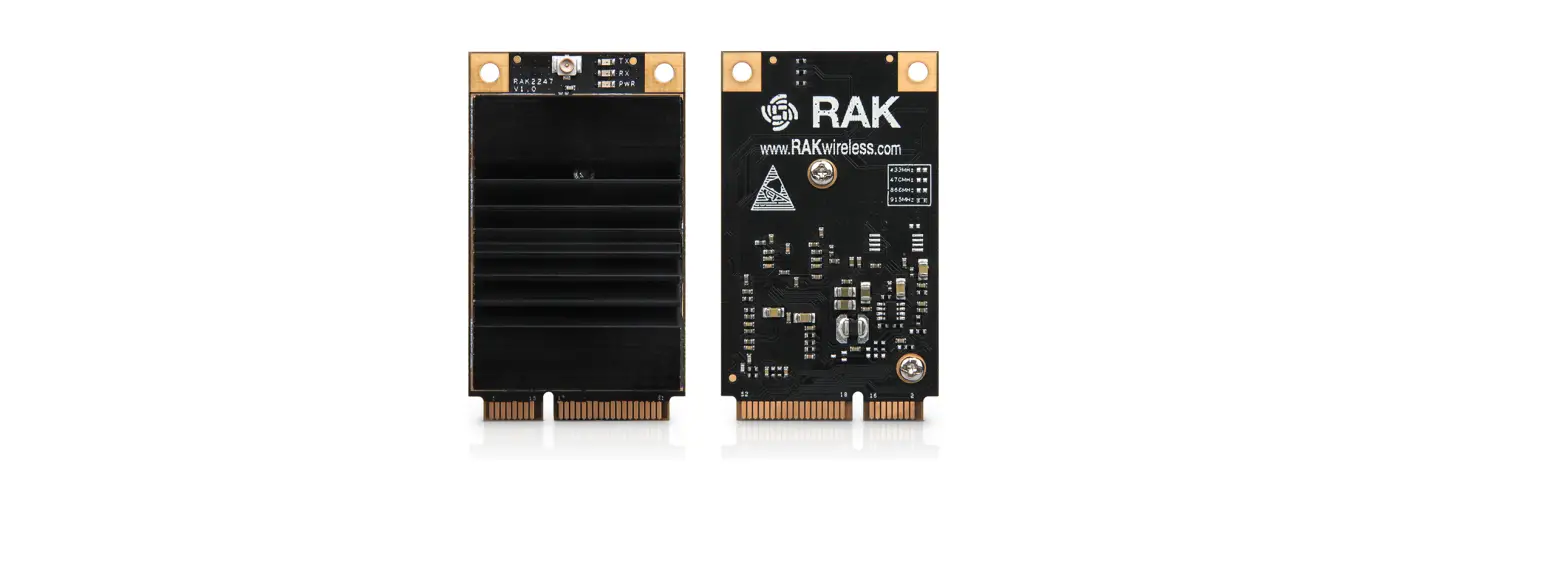
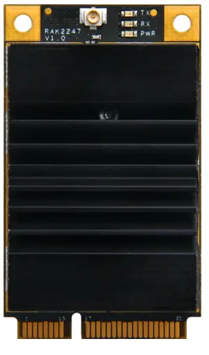
The RAK2247 is a LoRa concentrator module with the mini PCIe form factor based on SX1301, which enables an easy integration into an existing routers and others network equipment with LoRa Gateway capabilities.It can be used in any embedded platform offering a free mini-PCIe slot with SPI or USB connection.
RAK2247 is a complete and cost efficient LoRa gateway solution offering up to10 programmable parallel demodulation paths. It targets at smart metering fixed networks and Internet of Things applications with up to 500 nodes per km2 in moderately interfered environment. The modules have the industry standard PCI Express Mini Card form factor, which enables easy integration into an application board and is also ideal for manufacturing of small series.
The main features are listed below:
- Compatible with Mini PCI-e Edition specification with metal cooling
- SX1301 base band processor emulates 49 x LoRa demodulators 10 parallel demodulation
- 2 x SX125x Tx/Rx front-ends high/ low
- Build in FT2232H to convert SPI interface of SX1301 to 0.
- Voltage of Mini PCI-e is 3.3v, compatible with 3G/LTE card of Mini PCI-e
- Supports US915
- Supports optional SPI or USB interfaces.
Package Contents
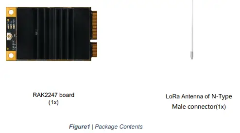
LoRa Concentrator Module RAK2247
Overview
Block Diagram
The block diagram of RAK2247-SPI shown as below
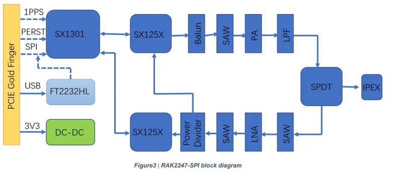
As described in Figure 3, the RAK2247 card integrates one SX1301 chip and two SX1255/7 and other chip for RF signal, which represents the core of the device, providing the related LoRa modem and processing functionallilies. Additional signal conditioning circuitry is implemented for PCI Express Mini Card compliance, and one UFL connectors are available for external antennas integration.
Operating Frequencies
The board supports all LoRaWAN frequency channels as below. Which is easy to configure while building the firmware from the source code.
Region: North America
Frequency ( MHz ) US: 923.3-927.5Mhz
Pin Definition
| No | Mini PCIEx PIN Rev. 2.0 | RAK2247 PIN | Power | I/O | Description | Remarks |
| 1 | WAKE# | NC | N/A | Internally not connected | ||
| 2 | 3.3Vaux | 3.3Vaux | 3.3Vaux | N/A | RAK2247power supply input | Connect to 3.3 V |
| 3 | COEX1 | NC | N/A | Internally not connected | ||
| 4 | GND | GND | GND | N/A | Ground | Connect to Ground |
| 5 | COEX2 | NC | N/A | Internally not connected | ||
| 6 | 1.5V | NC | N/A | Internally not connected | ||
| 7 | CLKREQ# | NC | N/A | Internally not connected | ||
| 8 | UIM_PWR | NC | N/A | Internally not connected | ||
| 9 | GND | GND | GND | N/A | Ground | Connect to ground |
| 10 | UIM_DATA | NC | N/A | Internally not connected | ||
| 11 | REFCLK- | NC | N/A | Internally not connected | ||
| 12 | UIM_CLK | NC | N/A | Internally not connected | ||
| 13 | REFCLK+ | NC | N/A | Internally not connected | ||
| 14 | UIM_RESET | NC | N/A | Internally not connected | ||
| 15 | GND | GND | GND | N/A | Ground | Connect to ground |
| 16 | UIM_SPU | NC | N/A | Internally not connected | ||
| 17 | UIM_IC_DM | NC(5V optional For PA) | N/A | Internally not connected |
| 18 | GND | GND | GND | N/A | Ground | Connect to ground |
| 19 | Reserved | 1PPS | N/A | Internal connection 1PPSfor SX1301 | ||
| 20 | W_DISABLE1# | NC | N/A | Internally not connected | ||
| 21 | GND | GND | GND | N/A | Ground | Connect to ground |
| 22 | PERST# | RESET | I | RAK2247 reset input | Active high(≥100ns) for SX1301 reset. | |
| 23 | PERn0 | NC | N/A | Internally not connected | ||
| 24 | 3.3Vaux | 3.3Vaux | 3.3Vaux | I | RAK2247 supply | Connect to 3.3 V |
| 25 | PERp0 | NC | N/A | Internally not connected | ||
| 26 | GND | GND | GND | N/A | Ground | Connect to ground |
| 27 | GND | GND | GND | N/A | Connect to ground | |
| 28 | 1.5V | NC | N/A | Internally not connected | ||
| 29 | GND | GND | GND | N/A | Ground | Connect to ground |
| 30 | SMB_CLK | NC | N/A | Internally not connected | ||
| 31 | PETn0 | NC | N/A | Internally not connected | ||
| 32 | SMB_DATA | NC | N/A | Internally not connected | ||
| 33 | PETp0 | NC | N/A | Internally not connected | ||
| 34 | GND | GND | GND | N/A | Ground | Connect to ground |
| 35 | GND | GND | GND | N/A | Ground | Connect to ground |
| 36 | USB_D- | USB_D- | USB | I/O | USB Data Line D- | 90-ohm nominal differential impedance. Pull-up, pull-down and series resistors as required by USB 2.0 specifications are part of the USB pin driver and need not be |
| 37 | GND | GND | GND | N/A | Ground | Connect to ground |
| 38 | USB_D+ | USB_D+ | USB | I/O | USB Data Line D+ | 90-ohm nominal differential impedance. Pull-up, pull-down and series resistors as required by USB 2.0 specifications are part of the USB pin driver and need not be |
| 39 | 3.3Vaux | 3.3Vaux | 3.3Vaux | I | RAK2247 supply | Connect to 3.3 V |
| 40 | GND | GND | GND | N/A | Ground | Connect to ground |
| 41 | 3.3Vaux | 3.3Vaux | 3.3Vaux | I | RAK2247 supply | Connect to 3.3 V |
| 42 | LED_WWAN# | NC | N/A | Internally not connected | ||
| 43 | GND | GND | GND | N/A | Ground | Connect to ground |
| 44 | LED_WLAN# | NC | N/A | Internally not connected | ||
| 45 | Reserved | PCIe_SCK | I/O | Host SPI CLK | Max 10MHz clock | |
| 46 | LED_WPAN# | NC | N/A | Internally not connected | ||
| 47 | Reserved | PCIe_MISO | I/O | Host SPI MISO | ||
| 48 | 1.5V | NC | N/A | Internally not connected | ||
| 49 | Reserved | PCIe_MOSI | I/O | Host SPI MOSI | ||
| 50 | GND | GND | GND | N/A | Ground | Connect to ground |
| 51 | W_DISABLE2# | PCIe_CSN | I/O | Host SPI CS |
| 52 | 3.3Vaux | 3.3Vaux | 3.3Vaux | I | RAK2247 supply | Connect to 3.3 V |
Power Supply
RAK2247 card must be supplied through the 3.3Vaux pins by a DC power supply. The voltage must be stable, because during this operation the current drawn from 3.3Vaux can vary significantly, based on the power consumption profile of the SX1301 chip (see SX1301 DS).
SPI Interface
A SPI interface is provided on the PCIe_SCK, PCIe_MISO, PCIe_MOSI, PCIe_CSN pins of the system connector. The SPI interface gives access to the configuration register of SX1301 via a synchronous full-duplex protocol. Only the slave side is implemented.
USB Interface
Note: RAK2247-SPI version don’t have this interface.
RAK2247 card can support the high speed USB to SPI by FT2232HL, it includes a high-speed USB 2.0 compliant interface with maximum 480 Mb/s data rate, representing the interface for any communication with an external host application processor. The module itself acts as a USB device and can be connected to any USB host equipped with compatible drivers. For more information, please refer to the data sheet of FT2232HL
1PPS
RAK2247 card includes the 1PPS input for received packets time-stamped.
RESET
RAK2247 card includes the RESET active-high input signal to reset the radio operations as specified by the SX1301 Specification
Antenna RF Interface
The modules have one RF interface over standard UFL connectors (Hirose U. FL-R-SMT) with a characteristic impedance of 50OHM. The RF port (J1) supports both Tx and Rx, providing the antenna interface
Electrical Characteristics
Stressing the device above one or more of the ratings listed in the Absolute Maximum Rating section may cause permanent damage. These are stress ratings only. Operating the module at these or at any conditions other than those specified in the Operating Conditions sections of the specification should be avoided.
Exposure to Absolute Maximum Rating conditions for extended periods may affect device reliability. The operating condition range define those limit within which the functionality of the device is guaranteed. Where application information is given, it is advisory only and does not form part of the specification.
Absolute Maximum Rating
Limiting values given below are in accordance with the Absolute Maximum Rating System (IEC 134)
| Symbol | Description | Condition | Min. | Max. |
| 3.3Vaux | Module supply voltage | Input DC voltage at 3.3Vaux pins | –0.3V | 3.6V |
| USB | USB D+/D- pins | Input DC voltage at USB interface pins | 3.6V | |
| SPDT_SEL | Port select | Input DC voltage at SPDT_SEL input pins | –0.3V | 3.6V |
| RESET | RAK2247 reset input | Input DC voltage at RESET input pin | –0.3V | 3.6V |
| SPI | SPI interface | Input DC voltage at SPI interface pin | –0.3V | 3.6V |
| GPS_PPS | GPS 1 pps input | Input DC voltage at GPS_PPS input pin | –0.3V | 3.6V |
| Rho_ANT | Antenna ruggedness | Output RF load mismatch ruggedness at ANT1 | 10:1VSWR | |
| Tstg | Storage Temperature | –40°C | 85°C | |
| Table 3 | Absolute maximum ratings |
The product is not protected against overvoltage or reversed voltages. If necessary, voltage spikes exceeding the power supply voltage specification, given in table above, must be limited to values within the specified boundaries by using appropriate protection devices
Operating Conditions
Input voltage at 3.3Vaux must be above the normal operating range minimum limit to switch on the module
| Symbol | Parameter | Min. | Typical | Max. |
| 3.3Vaux | Module supply operating input voltage14 | 3.00V | 3.30V | 3.60V |
Power Consumption
| Mode | Condition | Min | Type Max |
| Idle-Mode | All of the chip on the board enter idle mode or shutdown. | 68uA | |
| Active-Mode(TX) | TX enabledand RX disabled. | 440mA | |
| Active-Mode(RX ) | TX disabled and RX enabled. | 470mA |
RF Characteristics
The following table gives typically sensitivity level of the RAK2247 card.
| Signal Bandwidth/[KHz] | Spreading Factor | Sensitivity/[dBm] |
| 500 | 12 | -134 |
| 500 | 7 | -120 |
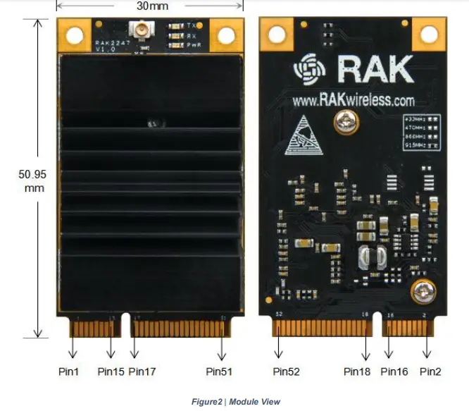
Mechanical Dimensions
RAK2247 card are fully compliant to the 52-pin PCI Express Full-Mini Card Type F2 form factor, with top-side and bottom-side keep-out areas, with 50.95 mm nominal length, 30 mm nominal width and all the other dimensions as defined by the PCI Express Mini Card Electromechanical Specification [9] except for the card thickness (nominal value is 3.7 mm), as described in the next figure.
The weight of the RAK2247 card is about 9.7 g.KHz
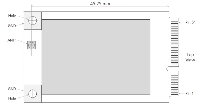
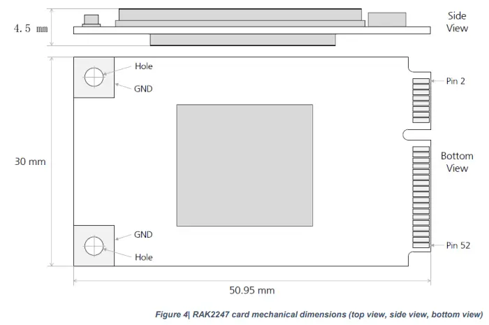
For further details regarding mechanical specifications see the PCI Express Mini Card Electromechanical Specification
LoRa Antenna
Overview
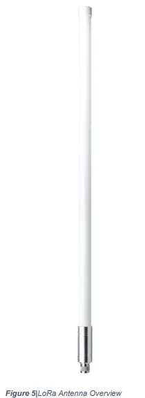
Antenna Parameter
| Items | Specifications |
| VSWR(Voltage Standard Wave Radio) | 1:1.5 |
| Gain | 5.8 dBi |
| WorkingTemperature&Humidity | T:-35 ºC ~ +80 ºC, H: 0% ~ 95% |
| StorageTemperature&Humidity | T:-40 ºC ~ +85 ºC, H: 0% ~ 95% |
Schematics Reference
RAK2247 card refer to Semtech’s reference design of SX1301, the SPI interface or USB interface, which convert SPI to USB2.0 by FT2232H, can be used on PCIE connector.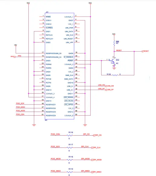
FCC Warning
This device complies with part 15 of the FCC Rules. Operation is subject to the following two conditions.
- This device may not cause harmful interference;
- This device must accept any interference received, including interference that may cause undesired
Any Changes or modifications not expressly approved by the party responsible for compliance could void the user’s authority to operate the equipment. When the module is installed in the host device, the FCC ID label must be visible through a window on the final device or it must be visible when an access panel, door or cover is easily removed. If not, a second label must be placed on the outside of the final device that contains the following text:
- Contains FCC ID: 2AF6B-RAK2247.
- Maximum antenna gain allowed for use with this device is 5.8 dBi.
This module complies with FCC radiation exposure limits set forth for an uncontrolled environment .This equipment should be installed and operated with minimum distance 20 cm between the radiator& your body.
Manufacture name and address:
Shenzhen Rakwireless Technology Co., Ltd.
Room 506, Bldg B, New Compark, Pingshan First Road, Taoyuan Street, XiLi town, Nanshan District, Shenzhen, China
Specific operational use conditions
This module is stand-alone modular. If the end product will involve the Multiple simultaneously transmitting condition or different operational conditions for a stand-alone modular transmitter in a host, host manufacturer have to consult with module manufacturer for the installation method in end system
Trace antenna designs
Not applicable
RF exposure considerations
To maintain compliance with FCC’s RF Exposure guidelines, This equipment should be installed and operated with minimum distance of 20cm from your body.
Antennas
This radio transmitter FCC ID: 2AF6B-RAK2247 has been approved by Federal Communications Commission to operate with the antenna types listed below, with the maximum permissible gain indicated. Antenna types not included in this list that have a gain greater than the maximum gain indicated for any type listed are strictly prohibited for use with this device
| Antenna Description | Antenna Type | Modullation Type | Impedance
(Ω) | Maximum antenna
gain(dBi) |
| Lora Antenna | Monopole | Chirp Modulation | 50 | 5.8dBi |
Label and compliance information
The final end product must be labeled in a visible area with the following” Contains FCC ID: 2AF6B-RAK2247”
Information on test modes and additional testing requirements
Host manufacturer is strongly recommended to confirm compliance with FCC requirements for the transmitter when the module is installed in the host.
Additional testing, Part 15 Subpart B disclaimer
Host manufacturer is responsible for compliance of the host system with module installed with all other applicable requirements for the system such as Part 15 B


