GOWIN DK-BLE-CEIT-ASSEM Development Kit
Introduction
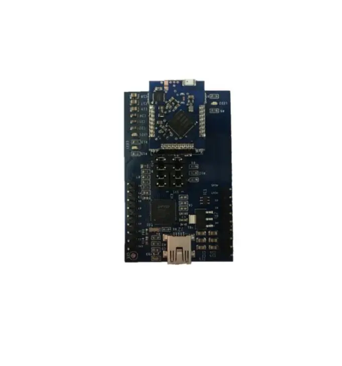
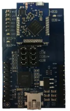
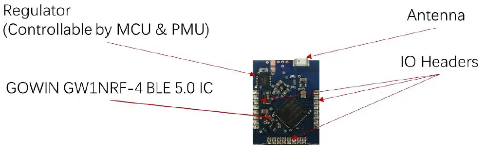
The DK-BLE-CEIT-ASSEM Development Kit is comprised of BLE module containing the GW1NRF-4 Bluetooth enabled µSoC FPGA along with a carrier board to quickly start developing applications. The GW1NRF-4 is the first device of its kind to offer a Bluetooth Low Energy 5.0 transceiver, a 32-bit ARC processor to hold the Bluetooth LE software stack as well as user applications and a 4.6k LUT of FPGA fabric for IO expansion, interfacing, parallel and accelerated gate array computing. The GW1NRF-LV4MOD/CEIT Bluetooth LE 5.0 module contains the GW1NRF-4 µSoC FPGA, radio antenna, and appropriate passives. The DK_BLE_CARRIER_INIT board provides a breakout of FPGA and microcontroller IO, LEDs for power and GPIO and an FTDI FT232H USB to JTAG device for easy programming. Figure 1 GW1NRF-4 BLE 5.0 Module (GW1NRF-LV4MOD/CEIT)
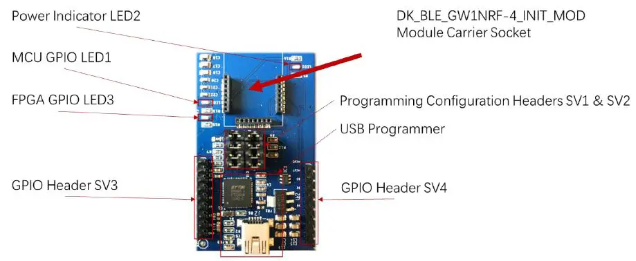
GW1NRF Carrier Board (DK_BLE_CARRIER_INIT)
Overview
The GW1NRF-4 module provides all passives, antenna as well as other components as a reference example. Bluetooth chips are typically developed on a module to enable an easier certification process. The GW1NRF-LV4MOD/CEIT module adopts GOWIN’s patented CoolStartTM technology, which allows power down of the FPGA IO and core voltages using the MCU PMU.
Note! FPGA pin assignments are labeled as they are defined in GOWIN EDA. MCU pin assignments are labeled as they are defined in GW1NRF SoC SDK, Synopsys Metaware and C/C++ definition files.
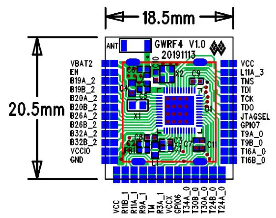
Table 1 – GW1NRF-LV4MOD/CEIT Header Pinouts and Description
| Header Pin Number | Signal Name | Description |
| L1 | VBAT | Battery Voltage Rail (1.9 – 3.6V); provides MCU and BLE VCC core voltage via built in Step Down DCDC |
| L2 | EN | Enable. Used to enable BLE and ARC power rails |
| L3 | B19A_2 | FPGA GPIO |
| L4 | B19B_2 | FPGA GPIO |
| L5 | B20A_2 | FPGA GPIO |
| L6 | B20B_2 | FPGA GPIO |
| L7 | B26A_2 | FPGA GPIO |
| L8 | B26B_2 | FPGA GPIO |
| L9 | B32A_2 | FPGA GPIO |
| L10 | B32B_2 | FPGA GPIO |
| L11 | VCCIO_FPGA | VCCIO for FPGA ( – ) |
| L12 | GND | Ground |
| B1 | VCC_GPIO | VCCIO for MCU ( – ) |
| B2 | R11B_1 | FPGA GPIO |
| B3 | R11A_1 | FPGA GPIO |
| B4 | R9A_1 | FPGA GPIO |
| B5 | TM | MCU GPIO 5 and/or MCU reset |
| B6 | R3A_1 | FPGA GPIO |
| B7 | VCCX | FPGA VCCX Voltage (2.5- 3.3V) |
| B8 | GPIO6 | MCU GPIO 6 |
| B9 | T34A_0 | FPGA GPIO |
| B10 | T30B_0 | FPGA GPIO |
| B11 | T30A_0 | FPGA GPIO |
| B12 | T24B_0 | FPGA GPIO |
| B13 | T24A_0 | FPGA GPIO |
| R1 | VCC | FPGA VCC core voltage (LV = 1.2V, UV = 1.8-3.3V) |
| R2 | L11A_3 | FPGA GPIO |
| Header Pin Number | Signal Name | Description |
| R3 | TMS | JTAG for FPGA and MCU |
| R4 | TDI | JTAG for FPGA and MCU |
| R5 | TDO | JTAG for FPGA and MCU |
| R6 | JTAGSEL | JTAG for FPGA and MCU |
| R7 | GPIO7 | MCU GPIO 7 |
| R8 | T9A_0 | FPGA GPIO |
| R9 | T9B_0 | FPGA GPIO |
| R10 | T16A_0 | FPGA GPIO |
| R11 | T16B_0 | FPGA GPIO |
The GW1NRF-4 Carrier Board provides LEDs attached to power, MCU and FPGA GPIOs, IO breakout of FPGA and MCU GPIOs, appropriate regulator for 5V to 3.3V conversion and a USB to JTAG circuit to program the device. It also provides programming headers to perform various methods of programming the device either through the USB to JTAG circuit or for wireless OTA (over-the-air) programming of the MCU and FPGA.
Note!
FPGA pin assignments are labeled as they are defined in GOWIN EDA. MCU pin assignments are labeled as they are defined in GW1NRF SoC SDK, Synopsys Metaware and C/C++ definition files.
Figure 4 – GW1NRF-4 BLE 5.0 Carrier Board Pinout
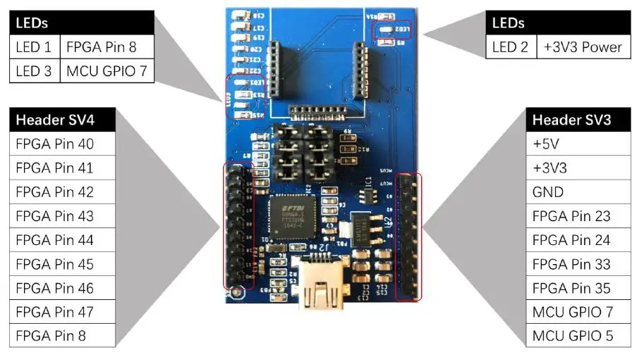
Table 2 – GW1NRF-4 BLE 5.0 Carrier Board Header Pinouts and Description
| LEDs | |
| LED 1 | LED connected to FPGA Pin 8 |
| LED 2 | LED connected to +3V3 Power Rail |
| LED 3 | LED connected to MCU GPIO 7 |
| Header SV4 (Left Side Header) | |
| FPGA Pin 40 | FPGA GPIO assigned to QFN pin 40 |
| FPGA Pin 41 | FPGA GPIO assigned to QFN pin 41 |
| FPGA Pin 42 | FPGA GPIO assigned to QFN pin 42 |
| FPGA Pin 43 | FPGA GPIO assigned to QFN pin 43 |
| FPGA Pin 44 | FPGA GPIO assigned to QFN pin 44 |
| FPGA Pin 45 | FPGA GPIO assigned to QFN pin 45 |
| FPGA Pin 46 | FPGA GPIO assigned to QFN pin 46 |
| FPGA Pin 47 | FPGA GPIO assigned to QFN pin 47 |
| Header SV3 (Right Side Header) | |
| +5V | 5.0V power rail from USB input |
| +3V3 | 3.3V power Rail from regulator output |
| GND | Ground |
| FPGA Pin 23 | FPGA GPIO assigned to QFN pin 23 |
| FPGA Pin 24 | FPGA GPIO assigned to QFN pin 24 |
| FPGA Pin 33 | FPGA GPIO assigned to QFN pin 33 |
| FPGA Pin 35 | FPGA GPIO assigned to QFN pin 35 |
| MCU GPIO 7 | MCU GPIO 7 |
| MCU GPIO 5 | MCU GPIO 5 |
Getting Started
The best place to start using the GW1NRF-4 Development Kit is the “GW1NRF_Getting_Started_v1” getting started package. The guide steps through programming the FPGA and MCU, synthesizing and compiling RTL and C/C++ code respectively and showing an example of how to communicate between the 32-bit ARC microprocessor and the FPGA fabric.
Schematic
DK_BLE_GW1NRF-4_INIT_MOD Schematic can be available at Gowin website: www.gowinsemi.com, Support > Starter Kits and Development Boards > GW1NRF-LV4MOD/CEIT.
DK_BLE_CARRIER_INIT Schematic
DK_BLE_CARRIER_INIT Schematic can be available at Gowin website: www.gowinsemi.com, Support > Starter Kits and Development Boards > DK BLE GW1NRF-4 INIT.
Support and Feedback
Gowin Semiconductor provides customers with comprehensive technical support. If you have any questions, comments, or suggestions, please feel free to contact us directly using the information presented below.
Website: www.gowinsemi.com E-mail: [email protected]
Revision History
| Date | Version | Description |
| 04/20/2020 | 1.0E | Preliminary Version |
Copyright © 2020 Guangdong Gowin Semiconductor Corporation. All Rights Reserved. No part of this document may be reproduced or transmitted in any form or by any denotes, electronic, mechanical, photocopying, recording or otherwise, without the prior written consent of GOWINSEMI.
Disclaimer
GOWINSEMI®, LittleBee®, Arora, and the GOWINSEMI logos are trademarks of GOWINSEMI and are registered in China, the U.S. Patent and Trademark Office, and other countries. All other words and logos identified as trademarks or service marks are the property of their respective holders, as described at www.gowinsemi.com.cn. GOWINSEMI assumes no liability and provides no warranty (either expressed or implied) and is not responsible for any damage incurred to your hardware, software, data, or property resulting from usage of the materials or intellectual property except as outlined in the GOWINSEMI Terms and Conditions of Sale. All information in this document should be treated as preliminary. GOWINSEMI may make changes to this document at any time without prior notice. Anyone relying on this documentation should contact GOWINSEMI for the current documentation and errata.


