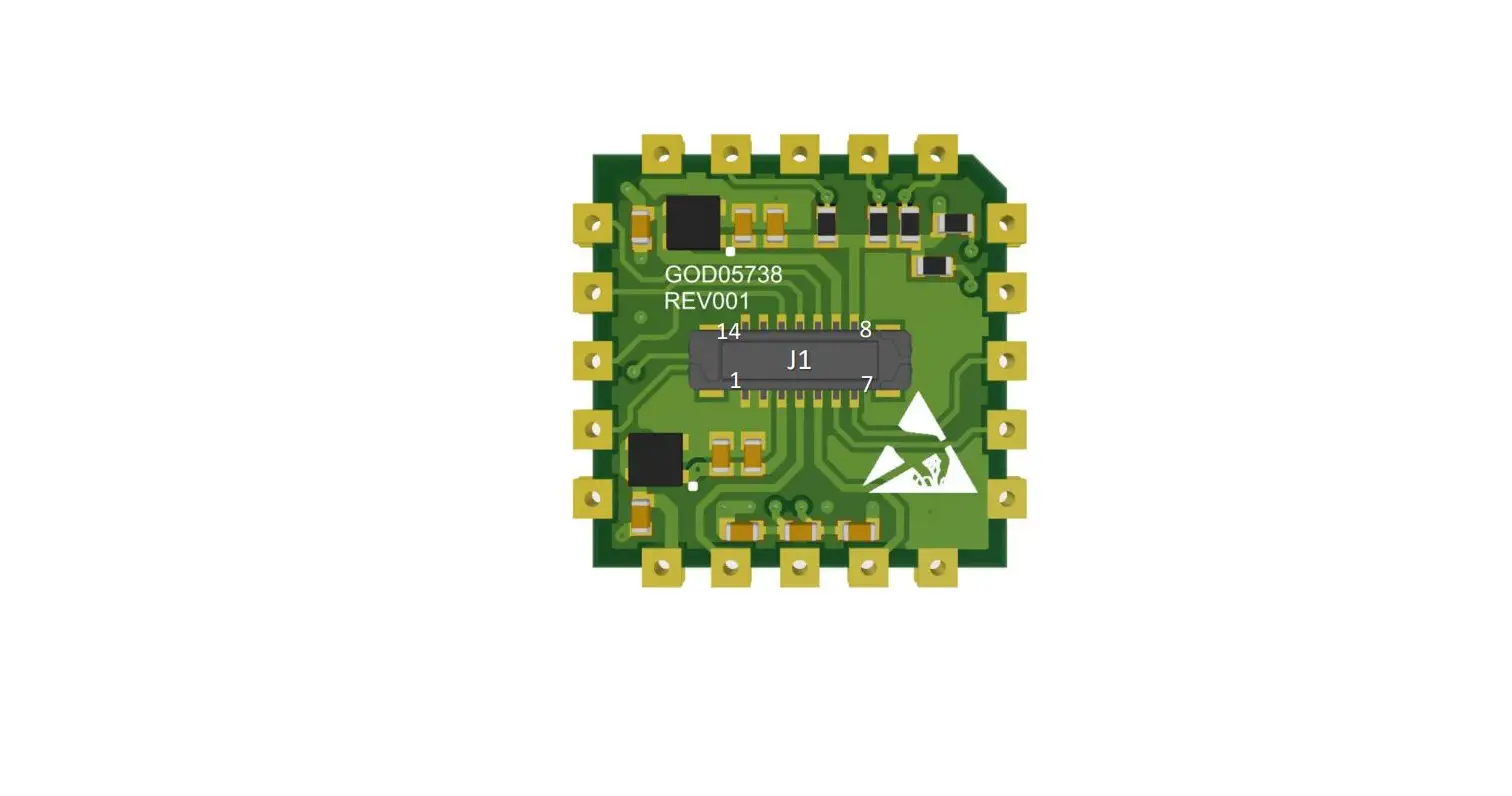
FUTEK QIA128 SPI Communication
General Description
The QIA128 is a single channel ultra-low power digital controller with UART and SPI outputs. The QIA128 (slave device) can be used to communicate with any master devices through an SPI bus.
Pin Configurations and Function Descriptions for QIA128
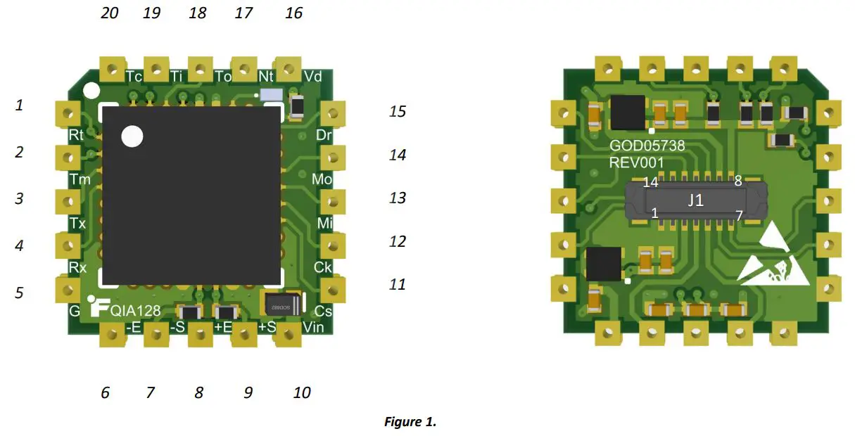 Table 1
| # | Pin | Description | J1 # |
| RESET | Active low reset pin. | – | |
| 2 | TMS | JTAG TMS (Test Mode Select). Input pin used for debug and download. | – |
| 3 | TX | Transmit Asynchronous Data output. | 7 |
| 4 | RX | Receive Asynchronous Data input. | 6 |
| 5 | GND | Ground pins are connected to each other internally. | 1 |
| 6 | -Excitation | Sensor excitation return (connected to Ground). | 2 |
| 7 | -Signal | Sensor negative Input. | 5 |
| 8 | +Excitation | Sensor excitation. | 3 |
| 9 | +Signal | Sensor positive Input. | 4 |
| 10 | VIN | Voltage input 3 − 5 | 9 |
| 11 | CS | Active low chip-select. Do not drive the line low until the device has booted up completely. Also ensure that the line is not driven low unless the ����� is low. | 14 |
| 12 | SCLK | Serial clock generated by master. | 13 |
| 13 | MISO | Master-In-Slave-Out. | 12 |
| 14 | MOSI | Master-Out-Slave-In. | 11 |
|
15 |
DRDY | Active low pin is used to keep all communication synchronized. It notifies the master device when new data from the sampling system is ready. This ensures that the master is always collecting the latest data. When the pin goes low, it indicates that the data is ready to be clocked out. This pin can be used to externally interrupt the master. The pin returns high when the system is in a conversion state and returns low once new data is ready. *Note: The pin does not return high once data is read—it will only return high once the system enters a conversion state. |
– |
| 16 | VDD | Digital rail (2.5V). | – |
| 17 | NTRST | JTAG NTRST/BM Reset/Boot Mode. Input pin used for debug and download only and boot mode (����). | – |
| 18 | TDO | JTAG TDO (Data Out). Input pin used for debug and download. | – |
| 19 | TDI | JTAG TDI (Data In). Input pin used for debug and download. | – |
| 20 | TCK | JTAG TCK (Clock Pin). Input pin used for debug and download. | – |
QIA128 SPI Configuration
TABLE 2
| Serial Word Length | 8-Bit | |||
| SPI Mode | Mode 0 (CPOL = 0, CPHA = 0) | |||
| SCLK Frequency | Min | 1 MHz | Max | 2 MHz |
| Internal Clock Frequency of MCU | 10.24 MHz | |||
| Operation Mode | Slave | |||
| Voltage Level | 1.8 VDC (compatible with 3.3 VDC) | |||
QIA128 Internal Design Algorithm
When the DRDY pin goes high, it means the device is in the process of A/D conversion, calculating the CRC8 (See CRC Calculations and References) and generating the packet that needs to be sent per the master device’s request. DRDY goes low as soon as it fills out the SPI TX buffer. The following algorithm is being executed while DRDY is high:
- Receives the latest ADC data from the highest interrupt priority
- Slave Service Function
- Keeps reading the RX FIFO until it is empty
- Saves all the bytes in a software buffer
- If the buffer is empty, creates a mock-up GADC command to go to the default state
- Checks the CRC8 byte and CMD byte
- If either the CRC8 or the CMD are incorrect
- Goes to the default state
- Else
- Replies with the corresponding packet (See Table 5.)
- Default State:
- Restarts the SPI module
- Calculates the CRC8
- Loads 4 bytes of data (including the latest ADC data and the CRC8 byte) into the TX FIFO buffer
- DRDY goes low
It is important to note that when a packet is clocked into the QIA128 via the MOSI line, the response to that packet must be clocked out in the very next DRDY period. If it is not clocked out in the next DRDY period, the response will be lost, and the system will go back to clocking out the ADC data.
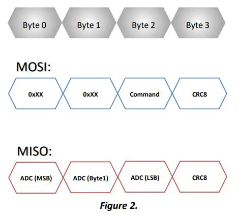
SPI Packet Structure
The packet structure stays consistent during all transactions and always includes four bytes of data for both receiving and transmitting.
“Continuous Read” Mode
GADC Command may be sent for each DRDY period to continuously get the ADC data.
*Note: If the CRC or the CMD bytes are incorrect, the device still fills out the buffer with the ADC data followed by the CRC8.
Timing Diagrams
Packet Structure (Get ADC Data):
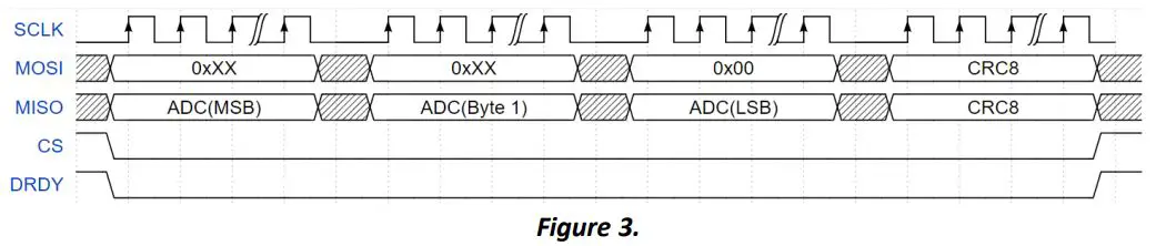 * Note: Each clock in Figure 3. represents 8-bits.
* Note: Each word (8-bits) can be clocked out with or without delay, but the entire transaction must be completed within a single DRDY period.
DRDY Period:
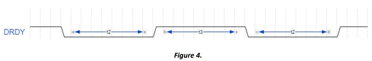 Table 3.
| (µ) | () | (µ) | Description |
| 240 | 4 SPS | ||
| 55 | 20 SPS | ||
| 19 | 50 SPS | ||
| 0 to …* | 9 | 125 | 100 SPS |
| 4.5 | 200 SPS | ||
| 1.5 | 500 SPS | ||
| 1.1 | 850 SPS | ||
| 0.6 | 1300 SPS |
*Note: No delay or any delay as long as all 4 bytes are clocked out prior to DRDY going high. (See 2 )
System Behavior
Start-up
When the system powers ON, it starts reading data from the internal flash and the solid green LED lights up; this
represents normal operation mode.
*Note: Do not drive the line low until the device has booted up completely. Also ensure that the line is not driven low unless the DRDY is low. The DRDY line goes low as soon as the first data is ready to be clocked out.
Sampling Rate Change
When a sampling rate change is requested, it will take certain amount of time (depends on the requested sampling rate) to
see the change in the DRDY period. (See Table 4.)
Table 4.
| Maximum Approximate data rate change timing () | SR Code | Sampling Rate |
|
≅250 | 0x00 | 4 SPS |
| 0x01 | 20 SPS | |
| 0x02 | 50 SPS | |
| 0x03 | 100 SPS | |
| 0x04 | 200 SPS | |
| 0x05 | 500 SPS | |
| 0x06 | 850 SPS | |
| 0x07 | 1300 SPS |
Command-Set List
Table 5.
|
Type |
Name |
Description | MOSI Line Packet Structure (Master to QIA128) | MISO Line Packet Structure (QIA128 to Master) | ||||||
| CMD | CRC | Payload | Payload | Payload | CRC | |||||
| Byte 0 | Byte 1 | Byte 2 | Byte 3 | Byte 0 | Byte 1 | Byte 2 | Byte 3 | |||
| Get | GADC | Get ADC Data | 0xXX | 0xXX | 0x00 | CRC8 | ADC MSB | ADC Byte1 | ADC LSB | CRC8 |
| Get | GCP0 | Get Calibration Point Zero | 0xXX | 0xXX | 0x01 | CRC8 | ADC MSB | ADC Byte1 | ADC LSB | CRC8 |
| Get | GCP1 | Get Calibration Point One | 0xXX | 0xXX | 0x02 | CRC8 | ADC MSB | ADC Byte1 | ADC LSB | CRC8 |
| Get | GCP2 | Get Calibration Point Two | 0xXX | 0xXX | 0x03 | CRC8 | ADC MSB | ADC Byte1 | ADC LSB | CRC8 |
| Get | GCP3 | Get Calibration Point Three | 0xXX | 0xXX | 0x04 | CRC8 | ADC MSB | ADC Byte1 | ADC LSB | CRC8 |
| Get | GCP4 | Get Calibration Point Four | 0xXX | 0xXX | 0x05 | CRC8 | ADC MSB | ADC Byte1 | ADC LSB | CRC8 |
| Get | GCP5 | Get Calibration Point Five | 0xXX | 0xXX | 0x06 | CRC8 | ADC MSB | ADC Byte1 | ADC LSB | CRC8 |
| Get | GCP6 | Get Calibration Point Six | 0xXX | 0xXX | 0x07 | CRC8 | ADC MSB | ADC Byte 1 | ADC LSB | CRC8 |
| Get | GCP7 | Get Calibration Point Seven | 0xXX | 0xXX | 0x08 | CRC8 | ADC MSB | ADC Byte1 | ADC LSB | CRC8 |
| Get | GCP8 | Get Calibration Point Eight | 0xXX | 0xXX | 0x09 | CRC8 | ADC MSB | ADC Byte1 | ADC LSB | CRC8 |
| Get | GCP9 | Get Calibration Point Nine | 0xXX | 0xXX | 0x0A | CRC8 | ADC MSB | ADC Byte1 | ADC LSB | CRC8 |
| Get | GCP10 | Get Calibration Point Ten | 0xXX | 0xXX | 0x0B | CRC8 | ADC MSB | ADC Byte1 | ADC LSB | CRC8 |
| Get | GCP11 | Get Calibration Point Eleven | 0xXX | 0xXX | 0x0C | CRC8 | ADC MSB | ADC Byte1 | ADC LSB | CRC8 |
| Get | GCP12 | Get Calibration Point Twelve | 0xXX | 0xXX | 0x0D | CRC8 | ADC MSB | ADC Byte1 | ADC LSB | CRC8 |
| Get | GCP13 | Get Calibration Point Thirteen | 0xXX | 0xXX | 0x0E | CRC8 | ADC MSB | ADC Byte1 | ADC LSB | CRC8 |
| Get | GCP14 | Get Calibration Point Fourteen | 0xXX | 0xXX | 0x0F | CRC8 | ADC MSB | ADC Byte1 | ADC LSB | CRC8 |
| Get | GCP15 | Get Calibration Point Fifteen | 0xXX | 0xXX | 0x10 | CRC8 | ADC MSB | ADC Byte1 | ADC LSB | CRC8 |
| Get | GCP16 | Get Calibration Point Sixteen | 0xXX | 0xXX | 0x11 | CRC8 | ADC MSB | ADC Byte1 | ADC LSB | CRC8 |
| Get | GCP17 | Get Calibration Point Seventeen | 0xXX | 0xXX | 0x12 | CRC8 | ADC MSB | ADC Byte1 | ADC LSB | CRC8 |
| Get | GCP18 | Get Calibration Point Eighteen | 0xXX | 0xXX | 0x13 | CRC8 | ADC MSB | ADC Byte1 | ADC LSB | CRC8 |
| Get | GCP19 | Get Calibration Point Nineteen | 0xXX | 0xXX | 0x14 | CRC8 | ADC MSB | ADC Byte1 | ADC LSB | CRC8 |
| Get | GCP20 | Get Calibration Point Twenty | 0xXX | 0xXX | 0x15 | CRC8 | ADC MSB | ADC Byte1 | ADC LSB | CRC8 |
| Get | GCP21 | Get Calibration Point Twenty-One | 0xXX | 0xXX | 0x16 | CRC8 | ADC MSB | ADC Byte1 | ADC LSB | CRC8 |
| Get | GCP22 | Get Calibration Point Twenty-Two | 0xXX | 0xXX | 0x17 | CRC8 | ADC MSB | ADC Byte1 | ADC LSB | CRC8 |
| Get | GSSN | Get Sensor Serial Number | 0xXX | 0xXX | 0x18 | CRC8 | SSN MSB | SSN Byte1 | SSN LSB | CRC8 |
| Get | GISN | Get Instrument Serial Number | 0xXX | 0xXX | 0x19 | CRC8 | ISN MSB | ISN Byte1 | ISN LSB | CRC8 |
| Get | GFRN | Get Firmware Revision Number | 0xXX | 0xXX | 0x1A | CRC8 | Major | Minor | Patch | CRC8 |
| Get | GDR | Get Data Rate | 0xXX | 0xXX | 0x1B | CRC8 | 0x00 | 0x00 | SR Code (See Table 4.) | CRC8 |
| Set | S4SPS | Set 4 Sample Per Second | 0xXX | 0xXX | 0x1C | CRC8 | 0x00 | 0x00 | 0x00 | CRC8 |
| Set | S20SPS | Set 20 Sample Per Second | 0xXX | 0xXX | 0x1D | CRC8 | 0x00 | 0x00 | 0x00 | CRC8 |
| Set | S50SPS | Set 50 Sample Per Second | 0xXX | 0xXX | 0x1E | CRC8 | 0x00 | 0x00 | 0x00 | CRC8 |
| Set | S100SPS | Set 100 Sample Per Second | 0xXX | 0xXX | 0x1F | CRC8 | 0x00 | 0x00 | 0x00 | CRC8 |
| Set | S200SPS | Set 200 Sample Per Second | 0xXX | 0xXX | 0x20 | CRC8 | 0x00 | 0x00 | 0x00 | CRC8 |
| Set | S500SPS | Set 500 Sample Per Second | 0xXX | 0xXX | 0x21 | CRC8 | 0x00 | 0x00 | 0x00 | CRC8 |
| Set | S850SPS | Set 850 Sample Per Second | 0xXX | 0xXX | 0x22 | CRC8 | 0x00 | 0x00 | 0x00 | CRC8 |
* Note: 0xXX = Don’t care
* Note: All pre-defined responses from each command that is sent on the MOSI line should be expected in the next DRDY period.
Packet and CRC Examples
The following transaction is the response to the GSSN command (Get Sensor Serial Number) that is being clocked out with the GADC command (Get ADC Data):
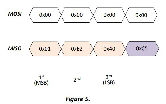 u8 crc8(u8 *p, u8 len); function (See CRC Calculations and References) has been used as a reference to calculate the CRC for the example above:
// CRC calculation for the MISO transaction, MSB = 0x01 and LSB = 0x40
u8 BUFFER[] = {MSB,…,LSB} »»» u8 BUFFER[] = {0x01, 0xE2, 0x40};
u8 crc8(BUFFER, 3);
then function returns 0xC5
ADC Data Conversion
The following formula could be used to convert the raw ADC data:
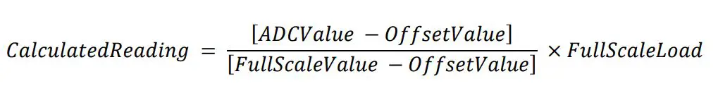 Here are the variables:
- DCVALUE= = the most recent analog-to-digital conversion value.
- OFFSETVALUE= = the analog-to-digital conversion value stored during calibration that corresponds to the offset (zero physical load).
- FULLSCALEVALUE= the analog-to-digital conversion value stored during calibration that corresponds to the full scale (maximum physical load)
- FULL SCA LOAD= the numeric value stored during calibration for the maximum physical load.
ADC Data Conversion Example
Calibration Data:
OffsetValue = Get Calibration Point Zero (GCP0): 8000000 (0x7A1200)
FullScaleValue = Get Calibration Point Five (GCP5): 12000000 (0xB71B00)
FullScaleLoad = 20 lb
ADCValue: Get ADC Data (GADC): 10552731 (0xA1059B)

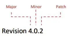
Firmware Revision
Firmware Notes
New Features
- Added new commands
- GND (Get Number of Directions)
- GNLP (Get Number of Loading Points)
- Replaced CRC16 by CRC8
- Package length has been decreased from 6 to 4
Changes
- LED indicator is changed from blinking to solid
- SPI command numbers are changed
Fixes: N/A
CRC Calculations and References
crc8.h example:
- extern uint8_t const crc_table[256];
- uint8_t crc8(uint8_t *p, uint8_t len);
crc8.c example:
uint8_t const crc_table[256] = { 0x00, 0x07, 0x0e, 0x09, 0x1c, 0x1b, 0x12, 0x15, 0x38, 0x3f, 0x36, 0x31, 0x24, 0x23, 0x2a, 0x2d, 0x70, 0x77, 0x7e, 0x79, 0x6c, 0x6b, 0x62, 0x65, 0x48, 0x4f, 0x46, 0x41, 0x54, 0x53, 0x5a, 0x5d, 0xe0, 0xe7, 0xee, 0xe9, 0xfc, 0xfb, 0xf2, 0xf5, 0xd8, 0xdf, 0xd6, 0xd1, 0xc4, 0xc3, 0xca, 0xcd, 0x90, 0x97, 0x9e, 0x99, 0x8c, 0x8b, 0x82, 0x85, 0xa8, 0xaf, 0xa6, 0xa1, 0xb4, 0xb3, 0xba, 0xbd, 0xc7, 0xc0, 0xc9, 0xce, 0xdb, 0xdc, 0xd5, 0xd2, 0xff, 0xf8, 0xf1, 0xf6, 0xe3, 0xe4, 0xed, 0xea, 0xb7, 0xb0, 0xb9, 0xbe, 0xab, 0xac, 0xa5, 0xa2, 0x8f, 0x88, 0x81, 0x86, 0x93, 0x94, 0x9d, 0x9a, 0x27, 0x20, 0x29, 0x2e, 0x3b, 0x3c, 0x35, 0x32, 0x1f, 0x18, 0x11, 0x16, 0x03, 0x04, 0x0d, 0x0a, 0x57, 0x50, 0x59, 0x5e, 0x4b, 0x4c, 0x45, 0x42, 0x6f, 0x68, 0x61, 0x66, 0x73, 0x74, 0x7d, 0x7a, 0x89, 0x8e, 0x87, 0x80, 0x95, 0x92, 0x9b, 0x9c, 0xb1, 0xb6, 0xbf, 0xb8, 0xad, 0xaa, 0xa3, 0xa4, 0xf9, 0xfe, 0xf7, 0xf0, 0xe5, 0xe2, 0xeb, 0xec, 0xc1, 0xc6, 0xcf, 0xc8, 0xdd, 0xda, 0xd3, 0xd4, 0x69, 0x6e, 0x67, 0x60, 0x75, 0x72, 0x7b, 0x7c, 0x51, 0x56, 0x5f, 0x58, 0x4d, 0x4a, 0x43, 0x44, 0x19, 0x1e, 0x17, 0x10, 0x05, 0x02, 0x0b, 0x0c, 0x21, 0x26, 0x2f, 0x28, 0x3d, 0x3a, 0x33, 0x34, 0x4e, 0x49, 0x40, 0x47, 0x52, 0x55, 0x5c, 0x5b, 0x76, 0x71, 0x78, 0x7f, 0x6a, 0x6d, 0x64, 0x63, 0x3e, 0x39, 0x30, 0x37, 0x22, 0x25, 0x2c, 0x2b, 0x06, 0x01, 0x08, 0x0f, 0x1a, 0x1d, 0x14, 0x13, 0xae, 0xa9, 0xa0, 0xa7, 0xb2, 0xb5, 0xbc, 0xbb, 0x96, 0x91, 0x98, 0x9f, 0x8a, 0x8d, 0x84, 0x83, 0xde, 0xd9, 0xd0, 0xd7, 0xc2, 0xc5, 0xcc, 0xcb, 0xe6, 0xe1, 0xe8, 0xef, 0xfa, 0xfd, 0xf4, 0xf3
};
// ————————————————————————————————-
uint8_t crc8(uint8_t *p, uint8_t len){
uint16_t i;
uint16_t crc = 0x0;
while (len–) {
i = (crc ^ *p++) & 0xFF;
crc = (crc_table[i] ^ (crc << 8)) & 0xFF;
}
return crc & 0xFF;
}//end crc8()
Sensor Solution Source
Load • Torque • Pressure • Multi Axis • Calibration • Instruments • Software


 Instructions")


