ON Semiconductor LV8811G Evaluation Board
NOTICE TO CUSTOMERS
The LV8811G, LV8813G, and LV8814J Evaluation Board is intended to be used for ENGINEERING DEVELOPMENT, DEMONSTRATION OR EVALUATION PURPOSES ONLY and is not considered by ON SEMICONDUCTOR to be a finished end product fit for general customer use. Information contained in this document regarding the device application and the like is provided only for your convenience. ON SEMICONDUCTOR MAKES NO REPRESENTATIONS OR WARRANTIES OF ANY KIND WHETHER EXPRESS OR IMPLIED, WRITTEN OR ORAL, STATUTORY OR OTHERWISE, RELATED TO THE INFORMATION, INCLUDING BUT NOT LIMITED TO ITS CONDITION, QUALITY, PERFORMANCE, MERCHANTABILITY OR FITNESS FOR PURPOSE. The user indemnifies ON SEMICONDUCTOR fully in respect of any claim made against ON SEMICONDUCTOR arising from the use of the LV8811G, LV8813G, and LV8814J Evaluation Board.
WARNING
The LV8811G, LV8813G, and LV8814J Evaluation Board is referenced to the DC supply ground and is not earthed. Hence, it carries a risk of electric shock. Caution is required when the power is applied to the kit. Only qualified technicians and/or engineers should handle the kit. When the power is applied to the kit, it is absolutely must that users only probe provided test points and do not touch any other point on the kit.
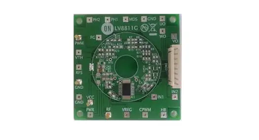
The LV8811G,LV8813G, and LV8814J Evaluation Board is designed to provide an easy and quick development platform for three phase single sensor BLDC motor control applications using LV8811G, LV8813G, nad LV8814J. The board enables users to develop their customized system solution by utilizing various features of LV8811G, LV8813G, and LV8814J and provides real-time development capabilities.
Overview
The LV8811G/13G/14J board consists of the following I/O and components:
- Three phases motor output
- Hall sensor bias output
- Hall sensor input
- PWM input
- FG output
- Monitoring outputs and setting inputs (optional)
- Configuration setting resistors
 LV8811G Evaluation Board
Features
The followings are key features of the board.
- Supports 12.0V (typ.) supply voltage
- Speed control input: PWM duty cycle
- Selectable Hall sensor type; sensor or IC
- Factory default: configured for sensor type
- Configureable minimum PWM duty cycle
- Factory-default:
14% for enable (start)
8% for disable (stop)
- Factory-default:
- Configurable lead angle range and its proportional constant to rotational speed
- Factory-default:
15degree at the lowest FG frequency
Lead angle = 0.15 × + 15
- Factory-default:
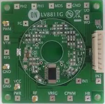
| Pin name | I/O | description |
| PWM | IN | Speed control PWM input. 20kHz – 50kHz 3Vpp The higher duty cycle gives the higher rotational speed. |
| FG | OUT | 3Vpp pulse whose frequency is proportional to motor speed |
| VTH | NA | Not applicable |
| RFS | Monitor | Current feedback signal can be monitored |
| GND | IN/OUT | Ground |
| VCC | IN | Power supply input. Typical 12V is assumed. |
| PWR | Floating | No connection |
| RF | Monitor | Power supply node for the power stage |
| VREG | OUT | 3V voltage regulator output |
| CPWM | Monitor | Triangle waveform of the PWM generator can be monitored |
| HB | OUT | Bias voltage output for a Hall sensor. 1.18V DC |
| IN1/IN2 | IN | Hall sensor signal input |
| U/V/W Out | OUT | Motor driver output |
| MDS | IN | Voltage level of MDS pin (minimum duty cycle setting) can be monitored. |
| PH1/PH2 | IN | Voltage level of PH1 and PH2 pins (lead angle setting) can be monitored. |
Quick Start
The following steps show the operation to spin a motor.
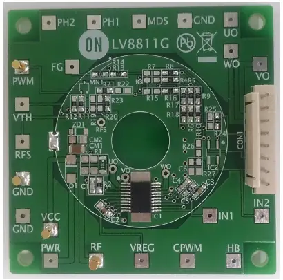
- step 1. Connect motor phases and Hall sensor bias, ground and signal outputs.
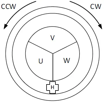
The rotational direction determination is shown in Table 2. Terminals are provided with: - For motor phases
- Through halls UO, VO and WO inside the circle,
- Pins UO, WO and VO, or
- Pin header CON1 pin 1, 2 and 3 for U, V and W individually (Hirose DF1-8)
- Hall sensor bias
- Pin HB and Pin GND
- Pin header CON1 pin 4 and 5 for HB and GND individually
- Hall sensor signal
- Pins IN1 and IN2
- Pin header CON1 pin 6 and 7 for IN1 and IN2 individually
- step 2. Connect PWM signal to PWM pin of the board.
The connection points, described in step 1 and 2, are shown in figure 2 and 3. - step 3. Set appropriate duty cycle of PWM.
- step 4. Connect power supply, and turn it on.
That’s all.
Hall sensor connection and rotational direction
| Motor Type | IN1 | IN2 | Direction |
| 3S2P 6S4P 12S8P | Hall minus | Hall plus | CW |
| 3S4P 6S8P 9S12P | Hall plus | Hall minus | CCW |
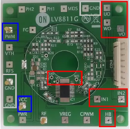 Key Input/Ouput Highlighted
 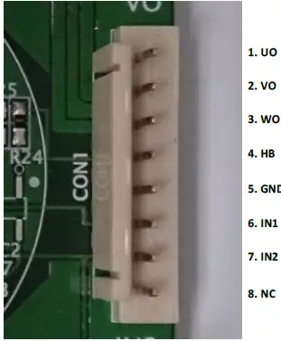 Pin header CON1
Minimum Duty Cycle Setting
To set the minimum duty cycle, a user needs to solder chip resistors.
The minimum duty cycle for disable (stop) DMIND is determined by the voltage level VMDS at MDS pin. 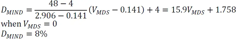 There is 6% of histeresisy between enable (start) and disable (stop) tarnsistions.
= + 6
The voltage level VMDS in this board is determined by resistors.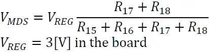
Lead angle tuning
To tune the lead angle, a user needs to solder chip resistors. The minimum lead angle at the lowest rotational speed P0 is determined by the voltage level VPH1 at PH1 pin.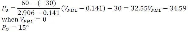 The lead angle P is dynamically adjusted with respect to FG frequency fFG.
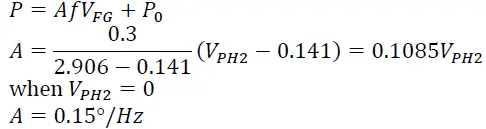 The voltage levels VPH1 and VPH2 in this board are determined by resistors.
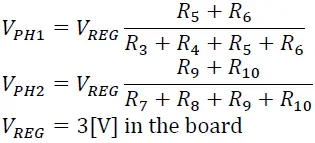
- The calculating formula of the adjustment of MDS and PH1,PH2 becomes the reference level. Please confirm real movement with a motor to use.
APPENDIX A: schematic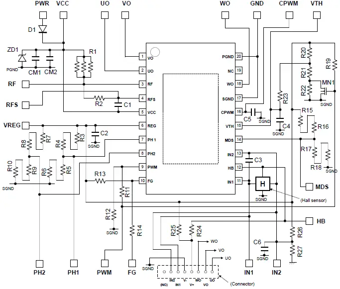 Notice: LV 8814J do not include the exposed-PAD
The hall sensor is not mounted on the board.
APPENDIX B: Bill of Material
| Part No. | Value | Part No. | Value |
| D1 | – | R11 | 1k_ohm |
| ZD1 | – | R12 | 10k_ohm |
| CM1 | 4.7uF | R13 | 4.7k_ohm |
| CM2 | – | R14 | 0_ohm |
| C1 | 1,500pF | R15 | – |
| C2 | 1uF | R16 | 1k_ohm |
| C3 | 0.01uF | R17 | 47k_ohm |
| C4 | 1,000pF | R18 | 1k_ohm |
| C5 | 0_ohm | R19 | – |
| C6 | – | R20 | – |
| CON1 | DF1- 8P-2.5DSA(05) | R21 | 1k_ohm |
| R1 | 0.1_ohm | R22 | – |
| R2 | 1k_ohm | R23 | 47k_ohm |
| R3 | – | R24 | 0_ohm |
| R4 | 1k_ohm | R25 | – |
| R5 | 47k_ohm | R26 | – |
| R6 | 1k_ohm | R27 | – |
| R7 | – | ||
| R8 | 1k_ohm | MN1 | – |
| R9 | 47k_ohm | ||
| R10 | 1k_ohm | – |
APPENDIX C: When speed adjustment is performed by VTH.
| Part No. | Value | Part No. | Value |
| D1 | – | R11 | – |
| ZD1 | – | R12 | 10k_ohm |
| CM1 | 4.7uF | R13 | 4.7k_ohm |
| CM2 | – | R14 | 0_ohm |
| C1 | 1,500pF | R15 | – |
| C2 | 1uF | R16 | 1k_ohm |
| C3 | 0.01uF | R17 | 47k_ohm |
| C4 | 1,000pF | R18 | 1k_ohm |
| C5 | 390pF | R19 | 0_ohm |
| C6 | – | R20 | 6.8k_ohm |
| CON1 | DF1- 8P-2.5DSA(05) | R21 | 1.8k_ohm |
| R1 | 0.2_ohm (x2) | R22 | 12k_ohm |
| R2 | 1k_ohm | R23 | 47k_ohm |
| R3 | – | R24 | 0_ohm |
| R4 | 1k_ohm | R25 | – |
| R5 | 47k_ohm | R26 | – |
| R6 | 1k_ohm | R27 | – |
| R7 | – | ||
| R8 | 1k_ohm | MN1 | 3LN01S (ON SEMI) |
| R9 | 47k_ohm | ||
| R10 | 1k_ohm | – |
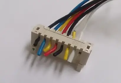
APPENDIX D: About COM1 connector.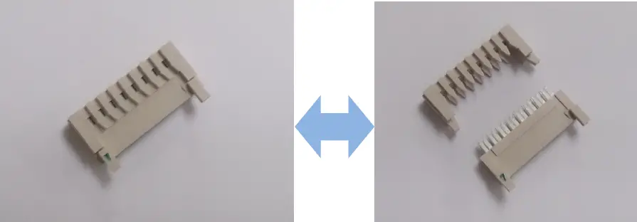
- An exclusive connector is attached to header COM1.
- When hooks of both sides are unlock, it divides into two parts.
- Wiring is pinched by two parts.
Photograph of completion example is shown below.