
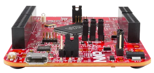
NXP FRDM-KE17Z Board
Overview
The Kinetis KE17Z freedom (FRDM-KE17Z) board is a standalone development platform that supports two microcontrollers
(MCUs): the target MCU and an open-standard serial and debug adapter (OpenSDA) MCU. The target MCU is MKE17Z256VLL7, which is a part of Kinetis E series of Arm® Cortex®-M0+ MCU product family. The OpenSDA MCU is a Kinetis K Series K20 family device, MK20DX128VFM5.
The FRDM-KE17Z board is compatible with the Arduino shields, the NXP FRDM-TOUCH board, and the NXP FRDM-MC-LVBLDC board.
The FRDM-KE17Z board comes preloaded with the bubble peripheral demo. The demo is available at the
boards\frdmke17z\demo_apps\bubble_peripheral folder of MCUXpresso SDK. The board is lead-free and RoHS-compliant.
This document provides detailed information about the FRDM-KE17Z board interfaces, power supplies, clocks, LEDs, sensors, and other interfaces.
Acronyms
The table below lists and explains the acronyms and abbreviations used in this document.
Table 1. Acronyms and abbreviations
| Term | Description |
| AWIC | Asynchronous Wake-up Interrupt Controller |
| ADC | Analog-to-digital converter |
| CLK | Clock |
| DIO | Data input/output |
| LPI2C | Low-power Inter-Integrated Circuit (I2C) |
| MCU | Microcontroller Unit |
| NMI | Non-maskable interrupt |
| OpenSDA | Open-standard serial and debug adapter |
| PWM | Pulse Width Modulation |
| SWD | Serial Wire Debug |
| TSI | Touch Sensing Input |
| USB | Universal Serial Bus |
| UART | Universal Asynchronous Receiver Transmitter |
| DNP | Do not populate |
Related documentation
The table below lists and explains the additional documents and resources that you can refer to for more information on FRDM-KE17Z. Some of the documents listed below may be available only under a non-disclosure agreement (NDA). To request access to these documents, contact your local field applications engineer (FAE) or sales representative.
Table 2. Related documentation
| Document | Description | Link/how to access |
| Kinetis KE17Z/13Z/12Z with up to 256 KB Flash Reference Manual | Intended for system software and hardware developers and applications programmers who want to develop products with this device. | Contact NXP FAE/sales representative |
| Kinetis KE17Z/13Z/12Z with up to 256 KB Flash Data Sheet | Provides information about electrical characteristics, hardware design considerations, and ordering information | Contact NXP FAE/sales representative |
| MCUXpresso Software Development Kit (SDK) documentation | MCUXpresso Software Development Kit (SDK) is a comprehensive software enablement package designed to simplify and accelerate application development with NXP MCUs based on Arm® Cortex® -M cores. | MCUXpresso Software Development Kit (SDK) documentation |
Kit contents
The table below lists the items included in the FRDM-KE17Z kit.
Table 3. Hardware kit contents
| Item | Quantity |
| FRDM-KE17Z board hardware assembly | 1 |
| USB Type A to micro-AB cable | 1 |
Block diagram
The figure below shows the FRDM-KE17Z block diagram.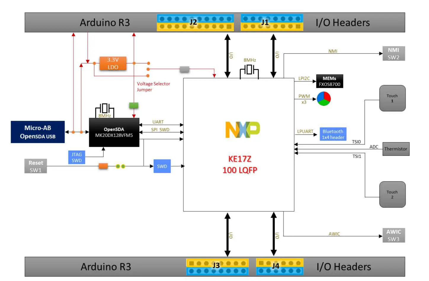 Board pictures
The figure below shows the top-side view of FRDM-KE17Z.
Figure 2. FRDM-KE17Z top view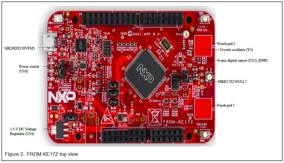 The figure below shows the onboard jumpers and connectors on FRDM-KE17Z.
Figure 3. FRDM-KE17Z jumpers and connectors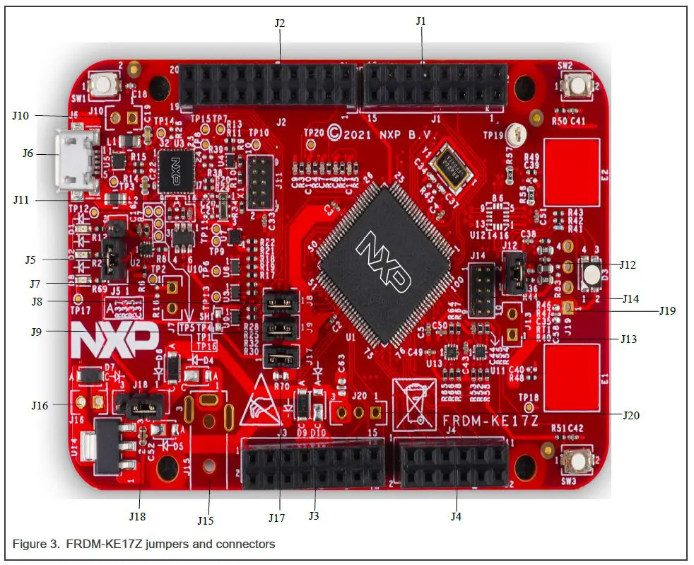 The figure below shows the LEDs and push buttons on FRDM-KE17Z.
Figure 4. FRDM-KE17Z LEDs and push buttons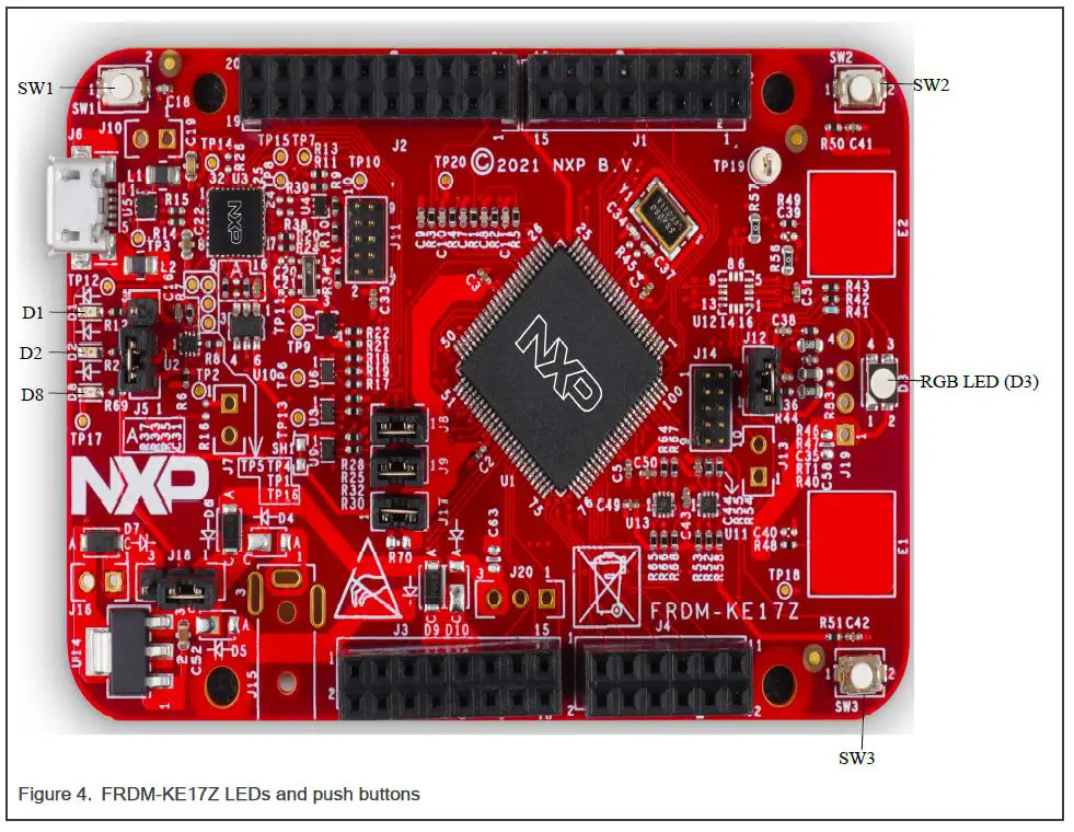 Board features
The table below lists the features of FRDM-KE17Z. Figure 2 shows different components of FRDM-KE17Z.
Table 4. FRDM-KE17Z features
| FRDM-KE17Z feature | Processor feature used | Description |
| MCU | MKE17Z256VLL7, 32-bit MCU core from Arm Cortex-M0+ class, 72 MHz CPU frequency NOTE For details on the MKE17Z256VLL7 MCU, see Kinetis KE17Z/13Z/12Z with up to 256 KB Flash Reference Manual. . | |
| Power supply | • 5 V input power via an external DC power supply, OpenSDA USB micro-AB connector, or I/O header, J3 |
| FRDM-KE17Z feature | Processor feature used | Description |
| • 3.3 V or 5 V for MKE17Z256VLL7 by setting J18 • 3.3 V for MK20DX128VFM5 | ||
| Clock | • 8 MHz crystal clock for MKE17Z256VLL7 • 8 MHz crystal clock for MK20DX128VFM5 • SWD_CLK for MKE17Z256VLL7 • SDA_JTAG_TCLK for JTAG connector • SWD_CLK_TGTMCU for SWD connector | |
| TSI touch pad | Touch Sensing Input (TSI) module | • Includes two touch electrodes to support TSI functions • Electrode 1 is connected to TSI0 Channel 8 and electrode 2 is connected to TSI1 Channel 20 |
| 6-axis digital sensor (DNP) | Low-power Inter-Integrated Circuit (LPI2C) module | NXP FXOS8700CQ: • Supports motion sensing with NXP FXOS8700CQ • 6-axis sensor with integrated linear accelerometer and magnetometer |
| Thermistor | High-speed analog-to-digital converter (ADC) | • Positive Temperature Coefficients (PTC) thermistor • Supports temperature from 90 °C to -20 °C |
| Debug | • Onboard OpenSDA circuit provides an SWD debug interface to MKE17Z256VLL7 • Supports micro-AB USB port to access serial port as console for debug • Supports JTAG connector to program and debug MK20DX128VFM5 • Supports SWD connector to program and debug MKE17Z256VLL7 | |
| Interrupt buttons | Supports 2 interrupt push buttons: • SW2/Button 0 is used to issue non-maskable interrupt (NMI) signal to MKE17Z256VLL7 • SW3/Button 1 is used to issue Asynchronous Wake-up Interrupt Controller (AWIC) interrupt signal to MKE17Z256VLL7 | |
| I/O headers | Headers compatible with: • Arduino shields • NXP FRDM-TOUCH • NXP FRDM-MC-LVBLDC |
| FRDM-KE17Z feature | Processor feature used | Description |
| RGB LED | Pulse Width Modulation (PWM) | • Supports RGB LED controlled by the embedded software application |
| Bluetooth header | LPUART | • Supports Bluetooth connectivity via Bluetooth header, J19 |
Push buttons
In addition to a Reset button for manually triggering a system reset, FRDM-KE17Z supports 2 interrupt push buttons. The following table explains the push buttons on FRDM-KE17Z. Figure 4 shows push buttons on FRDM-KE17Z.
Table 5. Reset and Interrupt push buttons
| Part identifier | Switch type | Description |
| SW1 | Push button | When pressed, resets MKE17Z256VLL7. Also, used to enter the OpenSDA bootloader mode. |
| SW2 | Push button | When pressed, generates non-maskable interrupt (NMI) signal to MKE17Z256VLL7. SW2/Button 0 is connected to the PTD3 pin on MKE17Z256VLL7. |
| SW3 | Push button | When pressed, issues Asynchronous Wake-up Interrupt Controller (AWIC) interrupt signal to MKE17Z256VLL7. SW3/Button 1 is connected to the PTE14 pin on MKE17Z256VLL7. |
Connectors
Connectors are onboard devices that allow to connect external devices to the board. Figure 3 shows the FRDM-KE17Z connectors. The table below describes the connectors.
Table 6. FRDM-KE17Z connectors
| Part identifier | Connector type | Description | Typical connection |
| J1 | 2×8 connector | I/O headers compatible with the Arduino shields, the NXP FRDM-TOUCH board, and the NXP FRDM-MC-LVBLDC board | |
| J2 | 2×10 connector | ||
| J3 | 2×8 connector | ||
| J4 | 2×6 connector | ||
| J6 | USB 2.0 micro- AB connector | Console port (port for connection with host computer) | Connects to USB Type A to micro-AB cable to connect to host computer |
| J19 | 1×4 connector | Bluetooth header | |
| J15 | DC power jack | Power connector | Connects to 5 V power adapter |
| J11 | 2×5 connector | OpenSDA JTAG connector | Debug interface to program and debug MK20DX128VFM5 |
| J14 | 2×5 connector | SWD connector | OpenSDA debug interface for target MCU, MKE17Z256VLL7 |
Jumpers
Jumpers (or shorting headers) are small connectors that allow to choose from two or more options available. Jumpers are installed during board assembly and do not require any changes. In FRDM-KE17Z, all jumpers are 2/3-pin connectors with two settings: open and shorted. Figure 3 highlights the FRDM-KE17Z jumpers available for use. The table below describes the jumpers.
The following is a list of all of the jumper options on FRDM-KE17Z.
Table 7. FRDM-KE17Z jumpers
| Part identifier | Jumper type | Description | Jumper settings |
| J5 | 1×3 header | Reset selection | • 1-2: OpenSDA sends reset to MKE17Z256VLL7 (default setting) • 2-3: SW1 sends reset to MKE17Z256VLL7. This setting is to be used when OpenSDA is not powered |
| J8 | 1×2 header | MCU SWD DIO signal | • Open: Disconnect MCU SWD_DIO to OpenSDA • Shorted: Connect MCU SWD_DIO to OpenSDA (default setting) |
| J9 | 1×2 header | MCU SWD CLK signal | • Open: Disconnect MCU SWD_CLK to OpenSDA • Shorted: Connect MCU SWD_CLK to OpenSDA (default setting) |
| J12 | 1×2 header | Thermistor | • Open: Test MCU current consumption • Shorted: Power supply for thermistor (default setting) |
| J13 | 1×2 header | OpenSDA debug interface | • Open: Isolates the onboard MCU from OpenSDA debug interface • Shorted (by a cut-trace on bottom layer): Connect the SWD_CLK signal from the SWD connector or OpenSDA to the MCU |
| J17 | 1×2 header | MCU VDD current measurement | • Open: Allow current measurement on MCU VDD • Shorted: Connect VDD to VDD_KE17Z (default setting) |
| J18 | 1×3 header | Power supply | • 1-2: MKE17Z256VLL7 MCU is 5 V powered (default setting) • 2-3: MKE17Z256VLL7 MCU is 3.3 V powered |
LEDs
FRDM-KE17Z has light-emitting diodes (LEDs) to monitor system functions, such as power-on, reset, board faults, and so on. The information collected from LEDs can be used for debugging purposes.
LEDs are highlighted in Figure 4. The table below describes the FRDM-KE17Z LEDs.
Table 8. FRDM-KE17Z LEDs
| Part identifier | LED color | LED name | Description (When LED in ON) |
| D2 | Yellow | SDA | Indicates OpenSDA status • Blinks: If MKE17Z256VLL7 is in Bootloader mode • ON: If an OpenSDA application is running |
| D1 | Red | Reset | Indicates Reset command is sent to MKE17Z256VLL7 via OpenSDA or when SW1 is pressed |
| Part identifier | LED color | LED name | Description (When LED in ON) |
| D3 | Red/Green/Blue | RGB | Controlled by the embedded software application. IC pins connected to RGB LED: • PTD11: RGB_GREEN • PTD12: RGB_BLUE • PTD10: RGB_RED |
| D8 | Green | Power | Indicates that FRDM-KE17Z is powered on |
FRDM-KE17Z Functional Description
This chapter describes the features and functions of FRDM-KE17Z. For details of the MKE17Z256VLL7 MCU features, see Kinetis KE17Z/13Z/12Z with up to 256 KB Flash Reference Manual.
The chapter is divided into the following sections:
- Power supplies
- Clocking
- TSI
- 6-axis digital sensor
- Thermistor
- OpenSDA
- Input/Output headers
- Bluetooth
Power supplies
FRDM-KE17Z can be powered with 5 V power supply via:
- an external DC power supply
- OpenSDA USB micro-AB connector
- I/O header, J3
The power supply devices on the board use the 5 V power to generate required power supplies for MKE17Z256VLL7,
SWD interface, I/O headers for Arduino shields, NXP FRDM-TOUCH board, and NXP FRDM-MC-LVBLDC, and numerous other peripherals.
Since, MKE17Z256VLL7 supports 2.7 V to 5.5 V power supply, MKE17Z256VLL7 can be powered 3.3 V or 5 V by setting J18. For details about setting J18, see Jumpers. However, OpenSDA MK20DX128VFM5 is always 3.3 V powered.
Primary power supply
FRDM-KE17Z can be powered up using one of the following ways:
Table 9. Primary power supply
| Part number | Description | Output power specifications |
| J15 | 5 V DC power jack | DC_JACK_5V_INPUT |
| ZX62-AB-5P (J6) | OpenSDA micro-AB USB connector provides 5 V power supply via power switch (U10) | P5V_SDA_PSW 5 V DC, 450 mA |
| J3 | I/O header provides 5 V power supply via a 5 V DC voltage regulator | P5V_LDO_OUT 5 V DC |
Secondary power supplies
The table below describes the FRDM-KE17Z power supply devices that generate secondary power supplies for the board.
| Reference designator | Device | Power supply voltage | Description |
| J6 | ZX62-AB-5P | P5V_SDA | • Power supply for power switch, MIC2005-0.8YM6 (P5V_SDA) • OpenSDA (P5V_SDA) • Unregulated power supply for MK20DX128VFM5[U3] (P5V_SDA) |
| U10 | MIC2005-0.8YM 6 (Microchip Technology) | P5V_SDA_PS W | • Power supply for FRDM-KE17Z (P5V_SDA_PSW). This power rail provides up to 450 mA of power at 5 V DC to FRDM-KE17Z • Power supply for I/O header, J3 (P5V_SDA_PSW) |
| (From 5 V power adapter, OpenSDA micro- AB USB connector, or I/O header) | VDD_5V (5 V DC) | • Power supply for 3.3 V DC voltage regulator, NCP1117ST33T3G [U14] • 5 V power supply for VDD if J18 is 1-2 | |
| U14 | NCP1117ST33T 3G (On Semiconductor) | P3V3 | • 3.3 V power supply for VDD if J18 is 2-3 • I/O header, J3 (P3V3) • 3.3 V power supply for voltage level translator, NTSX2102GU8H [U11, U13] (P3V3) • Power supply for FXOS8700CQ sensor |
| J18 | VDD = 5 V, if J18 is 1-2 VDD = 3.3 V, if J18 is 2-3 | VDD | • Power supply for Bluetooth header (VDD) • Power supply for interrupt push buttons (VDD) • Power supply for voltage level translator, NTSX2102GU8H [U11, U13] (VDD) • Power supply for I/O header, J3 (VDD) |
| J17 | VDD_KE17Z | • Power supply for MCU KE17Z (VDD_KE17Z) • Power supply for SWD connector (VDD_KE17Z) | |
| SH1 | V_TGTMCU | • Power supply for I/O, NTSX2102GU8H[U2], 74LVCH1T45[U6], 74LVC2T45GM,125[U7], 74LVCH1T45[U8], 74LVCH1T45[U9] (V_TGTMCU) | |
| L3 | VDDA | • Power supply for MCU KE17Z analog circuits (VDDA) • Power supply for thermistor RT1 (VDDA) | |
| L4 | VREFH | • Supply reference voltage for MCU KE17Z (VREFH) | |
| R71 | AREF | • Supply reference voltage for I/O header, J2 (AREF) |
| Reference designator | Device | Power supply voltage | Description |
| U3 | MK20DX128VF M5 | SDA_VOUT33 | • Regulator output voltage of MK20DX128VFM5 (SDA_VOUT33) • Power supply for OpenSDA (P3V3_SDA) • Power supply for OpenSDA JTAG connector (P3V3_SDA) • Power supply for voltage level translators, NTSX2102GU8H [U2], NL27WZ14MU1TCG [U4], 74LVCH1T45 [U6, U8, U9], 74LVC2T45GM [U7] (P3V3_SDA) |
Clocking
FRDM-KE17Z has the capability to run up to 72 MHz.
The table below provides details of different clocks of FRDM-KE17Z.
Table 10. FRDM-KE17Z clocks
| Clock generator | Clocks | Specifications | Destination |
| Crystal oscillator, Y1 | Crystal8M_XTAL Crystal8M_EXTAL | Frequency: 8 MHz | MKE17Z256VLL7: • Crystal8M_XTAL is connected to MKE17Z256VLL7 pin PTB6 • Crystal8M_EXTAL is connected to MKE17Z256VLL7 pin PTB7 |
| Crystal oscillator, X1 | SDA_XTAL SDA_EXTAL | Frequency: 8 MHz | OpenSDA: • SDA_XTAL is connected to MK20DX128VFM5 pin PTA19 • SDA_EXTAL is connected to MK20DX128VFM5 pin PTA18 |
| SWD connector | SWD_CLK | MKE17Z256VLL7: • Connected to MKE17Z256VLL7 pin PTC4 | |
| OpenSDA circuit | SDA_JTAG_TCLK | JTAG connector | |
| SWD_CLK_TGTMCU | SWD connector |
TSI
MKE17Z256VLL7 includes the Touch Sensing Input (TSI) module to detect capacitive touch sensor.
TSI is an electrode capacitive scan method based on the hardware. The basic element in capacitive touch sensing is the electrode. In this case, the electrode is an area of conductive material with dielectric material on the top, usually plastic or glass. This is what the user touches. This conductive area plus the dielectric material effectively create a capacitor referenced to the system ground. By touching the dielectric on top of the electrode, the user effectively changes the electrode capacitance both by adding a second conductive area that is grounded and by increasing the dielectric of the original capacitor. The sensor, or the TSI module in this case, uses a capacitive sensing method to measure changes in the electrode capacitance.
FRDM-TOUCH is a touch shield board for FRDM-KE17Z with capacitive touch buttons, slider, and rotary. This board can connect with FRDM-KE17Z and control the onboard RBG LED using keys, slider, and rotary touches.
FRDM-KE17Z includes two touch electrodes to support TSI functions in self-capacitive mode.
The touch electrode 1 is connected to TSI0 channel 8 and touch electrode 2 is connected to TSI1 channel 20.
Table 11. TSI touch pad connections
| Touch electrode | Touch pad | MKE17Z256VLL7 pin |
| Electrode 1 | TouchPad_0 | PTC5 |
| Electrode 2 | TouchPad_1 | PTC15 |
FRDM-KE17Z outputs TSI signals to headers J2 and J4 to support the FRDM-TOUCH board. FRDM-TOUCH includes four touch keys in a mutual-capacitive mode, touch slider, and rotary.
Table 12. TSI lane connections
| TSI channel | I/O header | Description | MKE17Z256VLL7 pin |
| TSI0_CH0 | J2[5] | PTE6 | |
| TSI0_CH1 | J2[3] | PTE2 | |
| TSI0_CH2 | J2[9] | PTA13 | |
| TSI0_CH3 | J2[7] | PTA12 | |
| TSI0_CH4 | J2[17] | TOUCH_M_TX_1 | PTA11 |
| TSI1_CH4 | PTA2 | ||
| TSI0_CH5 | J2[15] | TOUCH_M_TX_0 | PTA10 |
| TSI1_CH5 | PTA3 | ||
| TSI0_CH6 | J2[13] | TOUCH_M_RX_1 | PTE1 |
| TSI1_CH6 | PTD2 | ||
| TSI0_CH7 | J2[11] | TOUCH_M_RX_0 | PTE0 |
| TSI1_CH7 | PTD4 | ||
| TSI0_CH10 | J4[1] | TOUCH_S_0 | PTE10 |
| TSI1_CH10 | PTE7 | ||
| TSI0_CH11 | J4[3] | TOUCH_S_1 | PTD1 |
| TSI1_CH11 | PTA6 |
| TSI channel | I/O header | Description | MKE17Z256VLL7 pin |
| TSI0_CH12 | J2[19] | GND | PTD0 |
| TSI1_CH12 | PTA7 | ||
| TSI0_CH13 | J4[5] | TOUCH_S_2 | PTE16 |
| TSI1_CH13 | PTC8 | ||
| TSI0_CH14 | J4[7] | TOUCH_S_3 | PTE15 |
| TSI1_CH14 | PTC9 | ||
| TSI0_CH15 | J4[9] | TOUCH_S_4 | PTE13 |
| TSI1_CH0 | PTC6 | ||
| TSI0_CH16 | J4[11] | TOUCH_S_5 | PTE5 |
| TSI1_CH1 | PTC7 |
6-axis digital sensor
FRDM-KE17Z reserves an area (U12) to support motion sensing with NXP FXOS8700CQ 6-axis sensor with integrated linear accelerometer and magnetometer. FXOS8700CQ is a small, low-power, 3-axis, linear accelerometer and 3-axis, magnetometer combined into a single package.
FXOS8700CQ is connected to MKE17Z256VLL7 through an I2C interface, LPI2C0. The I2C address for FXOS8700CQ is 0x1C. Since, MKE17Z256VLL7 is 5 V powered by default, voltage level translators (U11, U13) are connected between MKE17Z256VLL7 and FXOS8700CQ to provide 3.3 V power supply to FXOS8700CQ.
Table 13. FXOS8700CQ pin connections
| FXOS8700CQ pin/signal | MKE17Z256VLL7 pin | Description |
| FXOS_SCL | PTB8 | I2C serial clock |
| FXOS_SDA | PTA16 | I2C serial data |
| FXOS_INT | PTB10 | Interrupt |
| FXOS_RST | PTB9 | Reset input |
Thermistor
FRDM-KE17Z includes a Positive Temperature Coefficients (PTC) thermistor with following features:
- Supports temperature from 90 °C to -20 °C
- THERM_0 is connected to the PTC1 pin on MKE17Z256VLL7
- THERM_1 is connected to the PTC0 pin on MKE17Z256VLL7
OpenSDA
OpenSDA is an open-standard serial and debug adapter.
The onboard MK20DX128VFM5 OpenSDA circuit bridges serial and debug communications between the USB host and MKE17Z256VLL7. The OpenSDA circuit provides an SWD debug interface to MKE17Z256VLL7. A standard USB A male to micro-AB male cable is used for debugging via the USB connector (J6).
The P&E debug application is an OpenSDA application that provides debugging and a virtual serial port all in one application. USB drivers for all P&E Microcomputer Systems debug tools are available at http://www.pemicro.com/opensda.
For details about the JTAG and SWD connectors, see Connectors.
The following table explains the OpenSDA signals connected to the target MCU (MKE17Z256VLL7).
Table 14. OpenSDA interface signals
| OpenSDA signals | MKE17Z256VLL7 pin | Description |
| RST_TGTMCU_b | PTA5 | Reset to target MCU |
| UART0_RX_TGTMCU | PTB0 | |
| UART0_TX_TGTMCU | PTB1 | |
| SWD_DIO_TGTMCU | PTA4 | Serial wire debug data input output |
| SWD_CLK_TGTMCU | PTC | Serial wire debug clock |
Input/Output headers
FRDM-KE17Z supports I/O headers compatible with the Arduino shields, the NXP FRDM-TOUCH board, and the NXP FRDM-MC-LVBLDC board. The following tables explain the pinouts for Arduino on FRDM-KE17Z.
Table 15. J2 connector (at left-upper side) pinouts for Arduino
| Pin | Arduino Functions | IC pin |
| 2 | Arduino_D8 | PTE11 |
| 4 | Arduino_D9 | PTB11 |
| 6 | Arduino_D10 | PTB5 |
| 8 | Arduino_D11 | PTB4 |
| 10 | Arduino_D12 | PTB3 |
| 12 | Arduino_D13 | PTB2 |
| 18 | Arduino_D14 | PTA16 |
| 20 | Arduino_D15 | PTB8 |
Table 16. J1 connector (at right-upper side) pinouts for Arduino
| Pin | Arduino Functions | IC pin |
| 2 | Arduino_D0 | PTD17 |
| 4 | Arduino_D1 | PTE12 |
| 6 | Arduino_D2 | PTD8 |
| 8 | Arduino_D3 | PTD9 |
| 10 | Arduino_D4 | PTC14 |
| 12 | Arduino_D5 | PTA15 |
| Pin | Arduino Functions | IC pin |
| 14 | Arduino_D6 | PTA17 |
| 16 | Arduino_D7 | PTA14 |
Table 17. J3 connector (at left-lower side) pinouts for Arduino
| Pin | Arduino Functions | IC pin |
| 6 | Arduino_RESET | PTA5 |
Table 18. J4 connector (at right-lower side) pinouts for Arduino
| Pin | Arduino Functions | IC pin |
| 2 | Arduino_A0 | PTC17 |
| 4 | Arduino_A1 | PTC16 |
| 6 | Arduino_A2 | PTD16 |
| 8 | Arduino_A3 | PTD15 |
| 10 | Arduino_A4 | PTA1 |
| 12 | Arduino_A5 | PTA0 |
Bluetooth
FRDM-KE17z supports 1×4 Bluetooth header, J19. J19 is connected to the MKE17Z256VLL7 through the LPUART1 interface. The following table shows the connections for the Bluetooth header Tx/Rx signals.
Table 19. Bluetooth header connections
| Bluetooth signal | MKE17Z256VLL7 pin | MKE17Z256VLL7 interface |
| BLUETOOTH_TX | PTD14 | LPUART1_TX |
| BLUETOOTH_RX | PTD13 | LPUART1_RX |
Appendix A
Revision History
The table below summarizes the revisions to this document. Table 20. Revision history
| Revision | Date | Topic cross-reference | Change description |
| Rev. 0 | 15 October 2021 | Initial public release |
How To Reach Us Home Page: nxp.com
Web Support: nxp.com/support
warranty
Limited warranty and liability — Information in this document is provided solely to enable system and software implementers to use NXP products. There are no express or implied copyright licenses granted hereunder to design or fabricate any integrated circuits based on the information in this document. NXP reserves the right to make changes without further notice to any products herein.
NXP makes no warranty, representation, or guarantee regarding the suitability of its products for any particular purpose, nor does NXP assume any liability arising out of the application or use of any product or circuit, and specifically disclaims any and all liability, including without limitation consequential or incidental damages. “Typical” parameters that may be provided in NXP data sheets and/or specifications can and do vary in different applications, and actual performance may vary over time. All operating parameters, including “typicals,” must be validated for each customer application by customer’s technical experts. NXP does not convey any license under its patent rights nor the rights of others. NXP sells products pursuant to standard terms and conditions of sale, which can be found at the following address: nxp.com/SalesTermsandConditions.
Right to make changes – NXP Semiconductors reserves the right to make changes to information published in this document, including without limitation specifications and product descriptions, at any time and without notice. This document supersedes and replaces all information supplied prior to the publication hereof.
Security — Customer understands that all NXP products may be subject to unidentified or documented vulnerabilities. Customer is responsible for the design and operation of its applications and products throughout their lifecycles to reduce the effect of these vulnerabilities on customer’s applications and products. Customer’s responsibility also extends to other open and/or proprietary technologies supported by NXP products for use in customer’s applications. NXP accepts no liability for any vulnerability. Customer should regularly check security updates from NXP and follow up appropriately. Customer shall select products with security features that best meet rules, regulations, and standards of the intended application and make the ultimate design decisions regarding its products and is solely responsible for compliance with all legal, regulatory, and security related requirements concerning its products, regardless of any information or support that may be provided by NXP. NXP has a Product Security Incident Response Team
(PSIRT) (reachable at [email protected]) that manages the investigation, reporting, and solution release to security vulnerabilities of NXP products.
NXP, the NXP logo, NXP SECURE CONNECTIONS FOR A SMARTER WORLD, COOLFLUX,EMBRACE, GREENCHIP, HITAG, ICODE, JCOP, LIFE, VIBES, MIFARE, MIFARE CLASSIC, MIFARE DESFire, MIFARE PLUS, MIFARE FLEX, MANTIS, MIFARE ULTRALIGHT, MIFARE4MOBILE, MIGLO, NTAG, ROADLINK, SMARTLX, SMARTMX, STARPLUG, TOPFET, TRENCHMOS, UCODE, Freescale, the Freescale logo, AltiVec, CodeWarrior, ColdFire, ColdFire+, the Energy Efficient Solutions logo, Kinetis, Layerscape, MagniV, mobileGT, PEG, PowerQUICC, Processor Expert, QorIQ, QorIQ Qonverge, SafeAssure, the SafeAssure logo, StarCore, Symphony, VortiQa, Vybrid, Airfast, BeeKit, BeeStack, CoreNet, Flexis, MXC, Platform in a Package, QUICC Engine, Tower, TurboLink, EdgeScale, EdgeLock, eIQ, and Immersive3D are trademarks of NXP B.V. All other product or service names are the property of their respective owners. AMBA, Arm, Arm7, Arm7TDMI, Arm9, Arm11, Artisan, big.LITTLE, Cordio, CoreLink, CoreSight, Cortex, DesignStart, DynamIQ, Jazelle, Keil, Mali, Mbed, Mbed Enabled, NEON, POP, RealView, SecurCore, Socrates, Thumb, TrustZone, ULINK, ULINK2, ULINK-ME, ULINK-PLUS, ULINKpro, µVision, Versatile are trademarks or registered trademarks of Arm Limited (or its subsidiaries) in the US and/or elsewhere. The related technology may be protected by any or all of patents, copyrights, designs and trade secrets. All rights reserved. Oracle and Java are registered trademarks of Oracle and/or its affiliates. The Power Architecture and Power.org word marks and the Power and Power.org logos and related marks are trademarks and service marks licensed by Power.org. M, M Mobileye and other Mobileye trademarks or logos appearing herein are trademarks of Mobileye Vision Technologies Ltd. in the United States, the EU and/or other jurisdictions.
For more information, please visit: http://www.nxp.com
For sales office addresses, please send an email to: [email protected]
References
 NXP® Semiconductors Official Site | NXP Semiconductors
-
Our Terms And Conditions Of Commercial Sale | NXP Semiconductors
-
Support | NXP Semiconductors
-
Domain Registered at Safenames
-
NXP® Semiconductors Official Site | NXP Semiconductors
-
Our Terms And Conditions Of Commercial Sale | NXP Semiconductors
-
Support | NXP Semiconductors
-
PEmicro | Experts in Embedded tools for Flash Programming and Development
-
MCUXpresso SDK | Software Development for Kinetis, LPC, and i.MX MCUs | NXP Semiconductors


