EBYTE E106-915G27P2 LoRa Gateway RF Module
EBYTE reserves all rights to this document and the information contained herein. Products, names, logos and designs described herein may in whole or in part be subject to intellectual property rights. Reproduction, use, modification or disclosure to third parties of this document or any part thereof without the express permission of EBYTE is strictly prohibited.
The information contained herein is provided “as is” and EBYTE assumes no liability for the use of the information. No warranty, either express or implied, is given, including but not limited, with respect to the accuracy, correctness, reliability and fitness for a particular purpose of the information. This document may be revised by EBYTE at any time. For most recent documents, visit www.ebyte.com.
Overview
Brief introduction
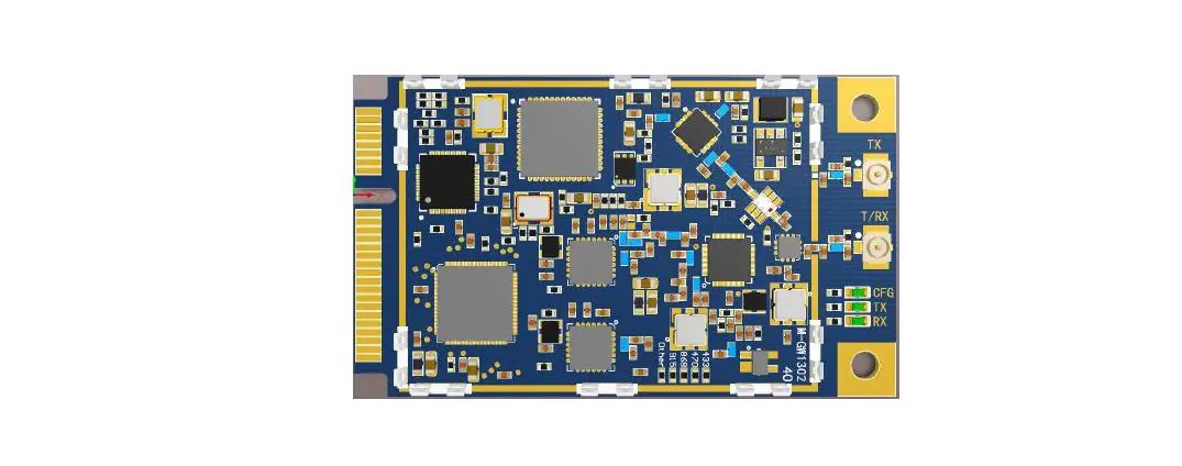
E106-915G27P2 module is a LoRa gateway RF module designed based on the SX1302 chip. It adopts the standard Mini PCI-e package, SPI interface, the module has built-in PA and LNA, and the half-duplex design is convenient for users to quickly develop LoRa gateway equipment.
SX1302 is a new generation LoRa gateway baseband chip launched by Semtech. It is equipped with front-end SX1250 and can support spreading factors SF5~SF12. Compared with the previous generation SX1301 gateway solution, it can support higher-speed data communication, while the power consumption is greatly reduced, the design is simplified, and the performance is significantly improved.
Main features
- PCI Express Mini Card 1.2 standard interface;
- Sending current max 360mA, receiving current 60mA;
- I-PEX antenna interface, half-duplex communication;
- Standard SPI digital interface;
- Support 8 receiving channels, SF5~SF12 full solution, receiving sensitivity as low as -141dBm;
- Support 1 transmission channel, the maximum transmission power is 27dBm (typical value 26dBm);
- ISM band:EU433、CN470、EU868、US915.
Block diagram Interface description
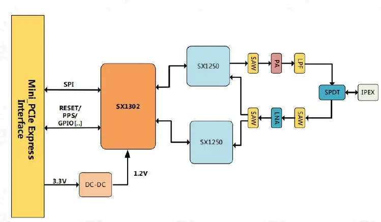 Interface description
Interface definition
The signal interface of E106-915G27P2 is standard Mini PCI Express interface. The following table gives the function definition and description of the 52pin corresponding to the module.
| Attribute | Description |
| DI | Digital input |
| DO | Digital output |
| IO | Bidirectional input and output |
| PI | Power input |
| Pin | Pin No. |
| GND | 4,9,15,18,21,26,27,29,34,35,37,40,43,50 |
| 3.3V | 2,24,39,41,52 |
| PPS | 19 |
| NRESET | 22 |
| RX_ON | 42 |
| TX_ON | 44 |
| CFG_ON | 46 |
| SX_SCK | 45 |
| SX_MISO | 47 |
| SX_MOSI | 49 |
| SX_CSN | 51 |
| No. | Mini PCIe definition | M-GW1302S definition | I/O attribute | Function description | Remark |
| 1 | WAKE# | RESERVED | DO | Use in transparent version, suspended | |
| 2 | 3.3Vaux | VCC_3V3 | PI | 3.3V DC Main power input | |
| 3 | COEX1 | NC | — | Internal use, suspended | |
| 4 | GND | GND | — | Ground | |
| 5 | COEX2 | NC | — | Internal use, suspended | |
| 6 | 1.5V | NC | — | Not used | |
| 7 | CLKREQ# | NC | — | Internal use, suspended | |
| 8 | UIM_PWR | NC | — | Not used | |
| 9 | GND | GND | — | Ground | |
| 10 | UIM_DATA | RESERVED | IO | Use in transparent version, suspended | |
| 11 | REFCLK- | RESERVED | DI | Use in transparent version, suspended | |
| 12 | UIM_CLK | RESERVED | IO | Use in transparent version, suspended | |
| 13 | REFCLK+ | RESERVED | DO | Use in transparent version, suspended | |
| 14 | UIM_RESET | NC | — | Not used | |
| 15 | GND | GND | — | Ground | |
| 16 | UIM_VPP | NC | — | Internal use, suspended | |
| 17 | RESERVED | NC | — | Internal use, suspended | |
| 18 | GND | GND | — | Ground | |
| 19 | RESERVED | PPS | DI | GPS time input, can be suspended | |
| 20 | W_DISABLE# | NC | — | Internal use, suspended | |
| 21 | GND | GND | — | Ground | |
| 22 | PERST# | NRESET | DI | Reset control pin, valid in high level | |
| 23 | PERn0 | RESERVED | DI | Reserved, externally suspended | |
| 24 | 3.3Vaux | VCC_3V3 | PI | 3.3V DC Main power input | |
| 25 | PERp0 | NC | — | Not used | |
| 26 | GND | GND | — | Ground | |
| 27 | GND | GND | — | Ground |
| 28 | 1.5V | NC | — | Not used | |
| 29 | GND | GND | — | Ground | |
| 30 | SMB_CLK | NC | — | Internal use, suspended | |
| 31 | PETn0 | RESERVED | DO | Reserved, externally suspended | |
| 32 | SMB_DATA | NC | — | Internal use, suspended | |
| 33 | PETp0 | NC | — | Not used | |
| 34 | GND | GND | — | Ground | |
| 35 | GND | GND | — | Ground | |
| 36 | USB_D- | RESERVED | IO | Use in transparent version, suspended | |
| 37 | GND | GND | — | Ground | |
| 38 | USB_D+ | RESERVED | IO | Use in transparent version, suspended | |
| 39 | 3.3Vaux | VCC_3V3 | PI | 3.3V DC Main power input | |
| 40 | GND | GND | — | Ground | |
| 41 | 3.3Vaux | VCC_3V3 | PI | 3.3V DC Main power input | |
| 42 | LED_WWAN# | RX_ON | DO | RX indication, connect to onboard LED | |
| 43 | GND | GND | — | Ground | |
| 44 | LED_WLAN# | TX_ON | DO | TX indication, connect to onboard LE | |
| 45 | RESERVED | SX_SCK | DI | SPI clock signal input | |
| 46 | LED_WPAN# | CFG_ON | DO | CFG indication, connect to onboard LE | |
| 47 | RESERVED | SX_MISO | DO | SPI data output | |
| 48 | 1.5V | NC | — | Not used | |
| 49 | RESERVED | SX_MOSI | DI | SPI data intput | |
| 50 | GND | GND | — | Ground | |
| 51 | RESERVED | SX_CSN | DI | SPI chip select signal input | |
| 52 | 3.3Vaux | VCC_3V3 | PI | 3.3V DC Main power input |
Power interface
| Item | Pin No | IO Attribute | Function description |
| GND | 4,9,15,18,21,26,27,29,34,35,37,40,43,50 | — | — |
| 3.3V | 2,24,39,41,52 | PI | 3.3V power input |
E106-915G27P2 module uses 3.3V power supply. In TX mode, the maximum instantaneous peak current may reach 400mA. In order to prevent voltage drop, the switch power supply or LDO used shall be able to provide enough current, and a tantalum capacitor or electrolytic capacitor with large capacitance value shall be added at the power supply port of the module. If switching power supply is used to supply power to the module, the circuit wiring shall avoid the antenna part as much as possible to prevent EMC interference.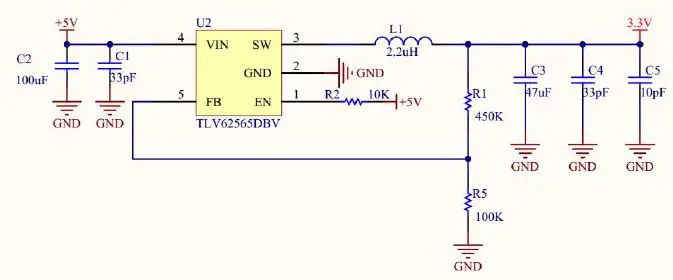
SPI interface
The SPI interface signal definition of E106-915G27P2 module is shown in the following table. Table 5: SPI interface signal definition
| Item | Pin No. | I/O attribute | Description | Voltage |
| SX_SCK | 45 | DI | SPI clock signal input | 3.3V |
| SX_MISO | 47 | DO | SPI data output | 3.3V |
| SX_MOSI | 49 | DI | SPI data input | 3.3V |
| SX_CSN | 51 | DI | SPI chip select signal input | 3.3V |
Control signal
| Item | Pin No. | I/O attribute | Description | Voltage |
| PPS | 11 | DI | GPS time input | 3.3V |
| NRESET | 13 | DI | Reset control pin | 3.3V |
| RX_ON | 42 | DO | RX signal indication | 3.3V |
| TX_ON | 44 | DO | TX signal indication | 3.3V |
| CFG_ON | 46 | DO | CFG signal indication | 3.3V |
. PPS signal
Support GPS-PPS input for receiving data packets with time stamp.
NRESET signal
The external control circuit can realize the reset of the module. The module can be reset by pulling up the NRESET level by 0.05~0.2s then releasing it. The NRESET signal is relatively sensitive to interference, and the wiring on the
module interface board should be as short as possible, and should be processed by certain ground.
RX_ON signal
When the receiving state of the module is turned on, this pin outputs a high level, and the on-board LED lights up at the same time, and connects to the GPIO of the SX1302.
TX_ON signal
When the module is transmitting data, this pin outputs a high level, and the on-board LED lights up, and connects to the GPIO of the SX1302.
CFG_ON signal
When the module successfully configures the parameters, this pin outputs a high level and the on-board LED lights up, and connects to the GPIO of the SX1302.
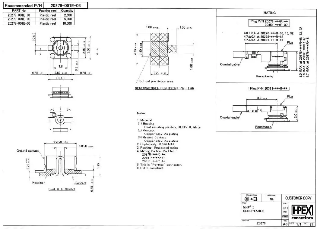
Antenna interface
The antenna connection base of the module adopts I-PEX 1 generation interface. Figure 3 shows the dimensions of the RF connector, in mm. Electrical and RF performance of the interface
 Electrical and RF performance of the interface
Power characteristics
The E106-915G27P2 module is powered by 3.3V, the input voltage is 3.3V±9%, and the power input must meet the current supply capacity of at least 500mA. The module input current requirements are shown in the following table:
| Item | Description | Min. Value | Typical value | Max. Value | Unit |
| VCC | Power supply voltage | 3.0 | 3.3 | 3.6 | V |
IO interface characteristics
The digital IO electrical characteristics of E106-915G27P2 module are shown in the table below. Table 8: IO interface electrical characteristics
| Item | Description | Min. Value | Max. Value | Unit |
| VIH | Input high voltage | 0.7*VCC | VCC+0.3 | V |
| VIL | Input low voltage | -0.3 | 0.3*VCC | V |
| VOH | Output high voltage | VCC-0.5 | VCC | V |
| VOL | Output low voltage | 0 | 0.4 | V |
Working current
| Item | Working condition | Working condition | Unit |
| RX | Turn on RX, disable TX | 54 | mA |
| TX/RX | Turn on Rx, turn on TX@25dBm | 360 | mA |
| IDLE | Idle mode | 27 | mA |
RF performance
| Working frequency | Maximum power value | Unit |
| 505.5MHz | 26 | dBm |
| 868.5MHz | 26 | dBm |
| 915.5MHz | 26 | dBm |
| Working frequency | Spreading factor(BW=125KHZ) | Receiving sensitivity (typical value dBm) |
|
475.5MHz | SF=5 | -121 |
| SF=7 | -127 | |
| SF=12 | -141 | |
|
868.5MHz | SF=5 | -121 |
| SF=7 | -127 | |
| SF=12 | -141 | |
|
915.5MHz | SF=05 | -121 |
| SF=07 | -127 | |
| SF=12 | -141 |
Dimensions
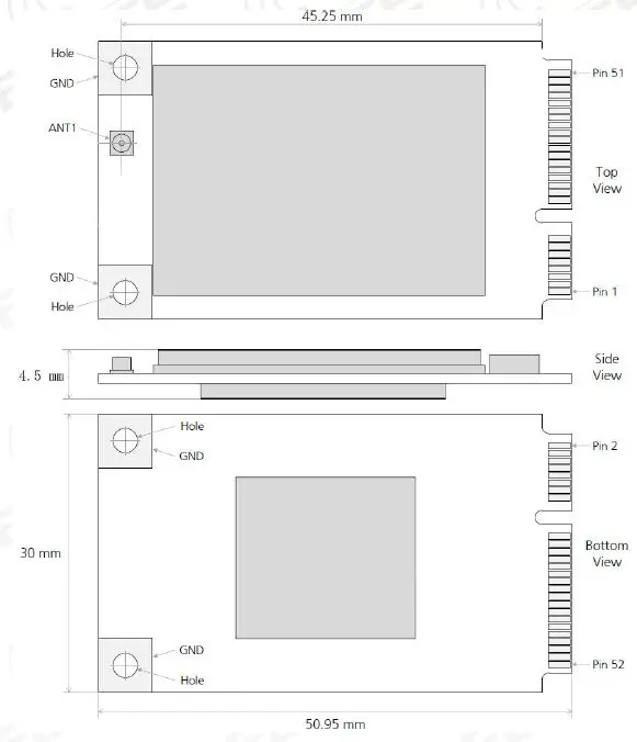
PCI Express mini card connectors that meet the standard can be used with this module, as shown in the following figure, MOLEX’s 679100002 connector.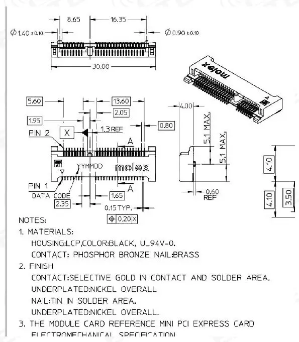
Internal connection
The following figure is the internal connection diagram of E106-915G27P2 for reference.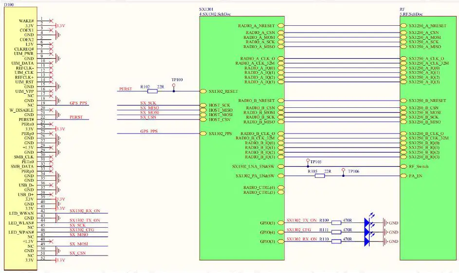
Reference design
E106-915G27P2 uses SPI interface to connect with the main control chip, and uses DC-DC to supply power to the module, and users can modify it as needed.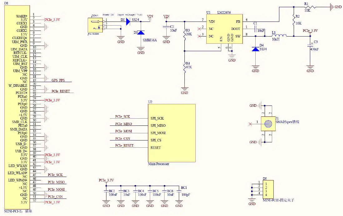
About us
Hotline: +96-4000-330-990 Tel: +96-028-61399028
Support: [email protected] Website: www.ebyte.com
Address: Building B5, Mould Industrial Park, 199# Xi-Qu Ave, West High-tech Zone, Chengdu, 611731, Sichuan, China