
EBYTE E78-900M22S1A ASR6505 868/915MHz LoRaWAN RF Module
Disclaimer
EBYTE reserves all rights to this document and the information contained herein. Products, names, logos and designs described herein may in whole or in part be subject to intellectual property rights. Reproduction, use, modification or disclosure to third parties of this document or any part thereof without the express permission of EBYTE is strictly prohibited. The information contained herein is provided “as is” and EBYTE assumes no liability for the use of the information. No warranty, either express or implied, is given, including but not limited, with respect to the accuracy, correctness, reliability and fitness for a particular purpose of the information. This document may be revised by EBYTE at any time. For most recent documents, Please visit www.ebyte.com
Overview
Introduction
The E78 series products are radio frequency transceiver modules with multiple frequency bands designed and produced by Ebyte, with long communication distance and extremely low current consumption in low power consumption mode. This module is a small-volume patch type (pinspacing 1.1mm). The E78 series products use ASR’s ASR6505 chip, which is a single-chip SoC integrated with ultra-low power LoRa, using Semtech’s advanced
low-power LoRa Transceiver SX1262, and integrates a STM8L152 low-power MCU, Flash capacity 64kB, SRAM Capacity 4kB, EEPROM capacity 2K, small size, ultra-low power consumption, support LoRaWAN, LinkWAN multiple protocol standards, suitable for a variety of Internet of Things application scenarios, is currently the best choice for LPWAN application chips. The E78 series products are hardware platforms and cannot be used independently. Users need to carry out secondary development. (We can customize standard LoRaWan and Ali linkWan nodes)
Features:
Under ideal test conditions, the communication distance can reach 5.5km; The maximum transmit power is 22dBm, and the software is multi-level adjustable; Support license-free ISM 868/915MHz frequency band; Support multiple modulation modes (GFSK Mode, LoRa); Support 1.8~3.7V power supply, power supply greater than 3.3V can guarantee the best performance; Industrial standard design, supporting long-term use at -40~+85℃;
Dual antennas are optional (IPX/PCB), which is convenient for users to develop and integrate; Based on the ASR6505 chip development, users can directly use it for secondary development.
Applications:
- Smart home and industrial sensors, etc.;
- Security system, positioning system;
- Wireless remote control, UAV;
- Wireless game remote control;
- Healthcare products;
- Wireless voice, wireless headset;
- Automotive industry applications.
Parameters
Limit Parameters:
| Main Parameters | Value | Notice | |
| Min. | Max. | ||
| Power supply voltage (V) | 0 | 3.9 | Over 3.9V will permanently burn the module |
| Blocking power (dBm) | – | 10 | The probability of burning is small when used at close range |
| Working temperature (℃) | -40 | +85 | Industrial grade |
Operating Parameters:
| Main Parameters | Value | Notice | ||||
| Min. | Typical | Max. | ||||
| Working voltage (V) | 1.8 | 3.3 | 3.7 | ≥3.3V can guarantee output power | ||
| Communication level (V) | – | 3.3 | – | Using 5V TTL is risky to burn | ||
| Working temperature (℃) | -40 | – | +85 | Industrial design | ||
| Working frequency (MHz) | 850 | 868/915 | 925 | Support ISM frequency band | ||
| Power | Emission current (mA) | – | 145 | – | Instantaneous power consumption | |
| Receiving current (mA) | – | 13 | – | – | ||
| Sleep current (μA) | – | 2.0 | – | Software shutdown | ||
| Maximum transmit power (dBm) | – | 21.5 | 22 | – | ||
| Receiving sensitivity (dBm) | -122 | -123 | -126 | The air rate is 595kbps | ||
| Air rate | LoRa(bps) | – | – | 62.5K | User programmable customization | |
| GFSK(bps) | – | – | 300K | User programmable customization | ||
| Parameters | Value | Notice |
| Ideal Range | 5500m | At Max TX power and 2.4kbps air rate, Two modules in a line of sight, clear weather, with 5dbi antennas at 2.5meters. |
| Crystal frequency | 32MHz | TXCO |
| Modulation | LoRa(recommended) | GFSK ,LoRa |
| Encapsulation method | SMA | – |
| Interface method | Stamp-hole | Diameter 1.1mm |
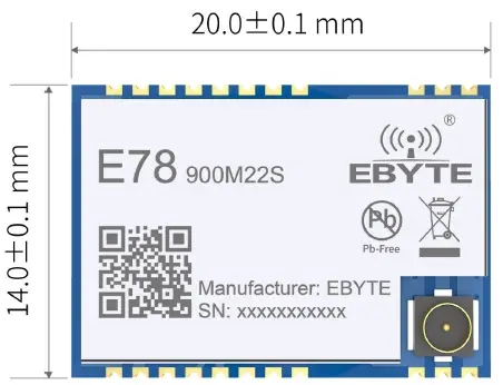
| Dimensions | 26*16mm | – |
| RF interface | IPEX/stamp-hole | Equivalent impedance is about 50Ω |
Hardware Notice:
- When designing the power supply circuit for the module, it is recommended to reserve more than 30% of the remaining amount, and the whole machine is beneficial for long-term stable operation;;
- The current required for the moment of launch is large but often because the launch time is extremely short, the total energy consumed may be smaller;
- When the customer uses an external antenna, the impedance matching degree between the antenna and the module at different frequency points will affect the magnitude of the emission current to varying degrees;
- The current consumed by the RF chip in the pure receiving state is called the receiving current. Some RF chips with communication protocols or developers have loaded some self-developed protocols on the whole machine, which may cause the receiving current of the test to be too large;
- When the customer uses an external antenna, the impedance matching degree between the antenna and the module at different frequency points will affect the magnitude of the emission current to varying degrees;
- The shutdown current is often much smaller than the current consumed by the power supply part of the whole machine at no load, without excessive demand;
- Due to the inherent error of the material itself, a single LRC component has an error of ±0.1%, but hesitant to use multiple LRC components in the entire RF loop, there will be accumulation of errors, resulting in differences in the emission current and the receiving current of different modules;
- Reducing the transmit power can reduce power consumption to a certain extent, but reducing the transmit power transmission for many reasons will reduce the efficiency of the internal PA.
Size and Pin definition
Size and Pin definition
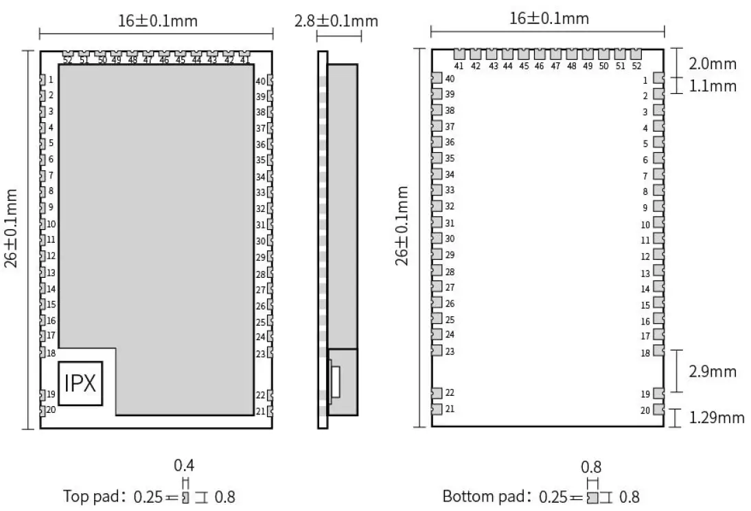
Pin definition
| No. | Name | Direction | Function |
| 1 | GND | – | Ground wire, connected to the power reference ground |
| 2 | LCD-SEG10 | Input/Output | MCU GPIO |
| 3 | LCD-SEG11 | Input/Output | MCU GPIO |
| 4 | LCD-SEG12 | Input/Output | MCU GPIO |
| 5 | LCD-SEG13 | Input/Output | MCU GPIO |
| 6 | LCD-SEG14 | Input/Output | MCU GPIO |
| 7 | LCD-SEG15 | Input/Output | MCU GPIO |
| 8 | LCD-SEG16 | Input/Output | MCU GPIO |
| 9 | LCD-SEG17 | Input/Output | MCU GPIO |
| 10 | I2C-SDA | Input/Output | I2C-SDA pin |
| 11 | I2C-SCL | Input/Output | I2C-SCL pin |
| 12 | ADC-IN0 | Input | ADC input pin |
| 13 | ADC-IN1 | Input | ADC input pin |
| 14 | GPIO2 | Input/Output | MCU GPIO |
| 15 | GPIO3 | Input/Output | MCU GPIO |
| 16 | GPIO4 | Input/Output | MCU GPIO |
| 17 | ADC_IN2 | Input | ADC input pin |
| 18 | GND | – | Ground wire, connected to the power reference ground |
| 19 | ANT | Output | Antenna interface, stamp hole (50 ohm characteristic impedance) |
| 20 | GND | – | Ground wire, connected to the power reference ground |
| 21 | GND | – | Ground wire, connected to the power reference ground |
| 22 | GND | – | Ground wire, connected to the power reference ground |
| 23 | GND | – | Ground wire, connected to the power reference ground |
| 24 | SPI-NSS | Input | SPI selection pin, external SPI can be selected |
| 25 | SPI-SCK | Input | SPI-SCK pin, can be used as external SPI |
| 26 | SPI_MISO | Output | SPI_MISO pin, can be used as external SPI |
| 27 | SPI_MOSI | Input | SPI MOSI pin, can be used as external SPI |
| 28 | LCD-SEG1 | – | MCU GPIO |
| 29 | LCD-SEG2 | Input/Output | MCU GPIO |
| 30 | SWIM | Input/Output | Programming pin |
| 31 | NRST | Input | External reset pin |
| 32 | LCD-COM0 | Input/Output | MCU GPIO |
| 33 | LCD-COM1 | Input/Output | MCU GPIO |
| 34 | LCD-COM2 | Input/Output | MCU GPIO |
| 35 | VREFP | Input | ADC reference voltage input |
| 36 | UART1-RX | Input | UART1-RX pin |
| 37 | UART1-TX | Output | UART1-TX pin |
| 38 | VLCD | Input | VLCD pin |
| 39 | LCD-SEG0 | Input/Output | MCU GPIO |
| 40 | GND | – | Ground wire, connected to the power reference ground |
| 41 | LCD-SEG3 | Input/Output | MCU GPIO |
| 42 | LCD-COM3 | Input/Output | MCU GPIO |
| 43 | LCD-SEG4 | Input/Output | MCU GPIO |
| 44 | LCD-SEG5 | Input/Output | MCU GPIO |
| 45 | UART0-RX | Input | UART0-RX pin |
| 46 | UART0-TX | Output | UART0-TX pin |
| 47 | LCD-SEG6 | Input/Output | MCU GPIO |
| 48 | LCD-SEG7 | Input/Output | MCU GPIO |
| 49 | LCD-SEG8 | Input/Output | MCU GPIO |
| 50 | LCD-SEG9 | Input/Output | MCU GPIO |
| 51 | VCC | – | Power supply, range 1.8V~3.7V (recommend to add ceramic filter capacitor) |
| 52 | GND | – | Ground wire, connected to the power reference ground |
| For more information about module pin definition, software driver and communication protocol, please see ASR6505 Datasheet | |||
Hardware and Software Guide
Hardware Design
- It is recommended to use a DC stabilized power supply to supply power to the module, and the power ripple coefficient should be as small as possible, and the module should be reliably grounded;
- Please pay attention to the correct connection of the positive and negative poles of the power supply. Reverse connection may cause permanent damage to the module;
- Please check the power supply to ensure that it is within the recommended power supply voltage. If it exceeds the maximum value, it will cause permanent damage to the module;
- Please check the stability of the power supply, and the voltage should not fluctuate greatly and frequently;
- When designing the power supply circuit for the module, it is often recommended to reserve more than 30% of the margin, and the whole machine is conducive to long-term stable operation;
- The module should be as far away as possible from the power supply, transformer, high-frequency wiring and other parts with large electromagnetic interference;
- High-frequency digital wiring, high-frequency analog wiring, and power wiring must avoid the bottom of the module. If it is necessary to pass under the module, assume that the module is soldered to the Top Layer, and the top ayer of the contact part of the module is covered with copper (all copper And well grounded), it must be close to the digital part of the module and routed in the Bottom Layer;
- Assuming that the module is soldered or placed on the Top Layer, it is also wrong to randomly route the wires on the Bottom Layer or other layers, which will affect the stray and receiving sensitivity of the module to varying degrees;
- Assuming that there are devices with large electromagnetic interference around the module, it will greatly affect the performance of the module. According to the intensity of the interference, it is recommended to stay away from the module. If the situation permits, proper isolation and shielding can be done;
- Assuming that there are traces with large electromagnetic interference around the module (high-frequency digital, high-frequency analog, power wiring), it will also greatly affect the performance of the module. According to the intensity of the interference, it is recommended to stay away from the module. Isolation and shielding;
- If the communication line uses 5V level, a 1k-5.1k resistor must be connected in series (not recommended, there is still a risk of damage);
- Try to stay away from part of the physical layer that is also 2.4GHz TTL protocol, for example: USB3.0;
- The antenna installation structure has a great impact on the performance of the module. Make sure that the antenna is exposed, preferably vertically upward. When the module is installed inside the case, a high-quality antenna extension cable can be used to extend the antenna to the outside of the case;
Software Writing
- This module is SX1262+STM8L152 integrated, and its driving method is completely equivalent to SX1262, and users can operate according to SX1262 or ASR6505 chip book;
- At the same time, please refer to the E78-900M22S1A and E78-900TBL-01A pin corresponding STM8 data provided by our company during the secondary development.
- The voltage range of the active crystal oscillator is 1.8V to 3V. 2.2V is recommended. 3.3V may be damaged.
Programming Diagram and Guide
E78-900M22S1A burning interface
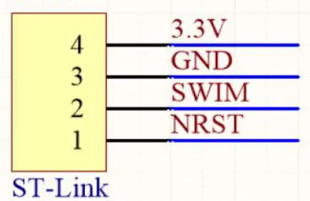
Connect the module pins 30 and 31, and use ST-LINK or STM8 debugging tools to download the program.
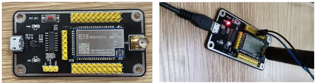
For secondary development, you are recommended to use test kit E78-900TBL-01A. It is convenient and efficient. First, power the module through the serial port of the test kit, and then connect the NRST pin and SWIM pin of ST-LINK to the test kit to download the program. As shown above.
Production guidance
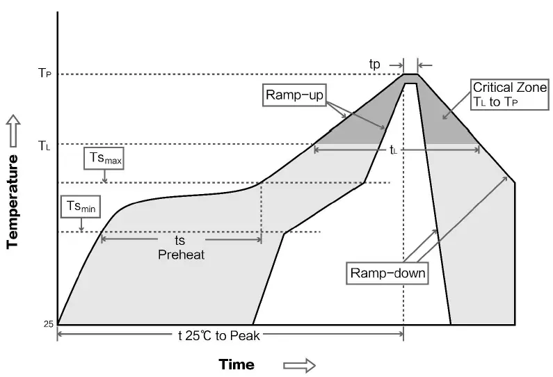
Reflow soldering temperature
| Profile Feature | Curve characteristics | Sn-Pb Assembly | Pb-Free Assembly |
| Solder Paste | Solder paste | Sn63/Pb37 | Sn96.5/Ag3/Cu0.5 |
| Preheat Temperature min (Tsmin) | Min preheating temp. | 100℃ | 150℃ |
| Preheat temperature max (Tsmax) | Mx preheating temp. | 150℃ | 200℃ |
| Preheat Time (Tsmin to Tsmax)(ts) | Preheating time | 60-120 sec | 60-120 sec |
| Average ramp-up rate(Tsmax to Tp) | Average ramp-up rate | 3℃/second max | 3℃/second max |
| Liquidous Temperature (TL) | Liquid phase temp. | 183℃ | 217℃ |
| Time(tL)Maintained Above(TL) | Time below liquid phase line | 60-90 sec | 30-90 sec |
| Peak temperature(Tp) | Peak temp. | 220-235℃ | 230-250℃ |
| Average ramp-down rate(Tp to Tsmax) | Average ramp-down rate | 6℃/second max | 6℃/second max |
| Time 25℃ to peak temperature | Time to peak temperature for 25℃ | 6 minutes max | 8 minutes max |
Reflow soldering curve
FAQ
Communication range is too short
- The communication distance will be affected when obstacle exists.
- Data lose rate will be affected by temperature, humidity and co-channel interference.
- The ground will absorb and reflect wireless radio wave, so the performance will be poor when testing near ground.
- Sea water has great ability in absorbing wireless radio wave, so performance will be poor when testing near the sea.
- The signal will be affected when the antenna is near metal object or put in a metal case.
- Power register was set incorrectly, air data rate is set as too high (the higher the air data rate, the shorter the distance).
- The power supply low voltage under room temperature is lower than 2.5V, the lower the voltage, the lower the transmitting power.
- Due to antenna quality or poor matching between antenna and module.
Module is easy to damage
- Please check the power supply source, ensure it is 2.0V~3.6V, voltage higher than 3.6V will damage the module.
- Please check the stability of power source, the voltage cannot fluctuate too much.
- Please make sure antistatic measure are taken when installing and using, high frequency devices have electrostatic susceptibility.
- Please ensure the humidity is within limited range, some parts are sensitive to humidity.
- Please avoid using modules under too high or too low temperature.
BER (Bit Error Rate) is high
- There are co-channel signal interference nearby, please be away from interference sources or modify frequency and channel to avoid interference;
- Poor power supply may cause messy code. Make sure that the power supply is reliable.
- The extension line and feeder quality are poor or too long, so the bit error rate is high;
Revision history
| Version | Date | Description | Issued by |
| 1.0 | 2021-03-1 | Initial version | Linson |
About us
- Website: www.ebyte.com
- Sales: [email protected]
- Support: [email protected]
- Tel: +86-28-61399028 Ext. 812
- Fax: +86-28-64146160
Address: Innovation Center B333~D347, 4# XI-XIN road,High-tech district (west), Chengdu, Sichuan, China


