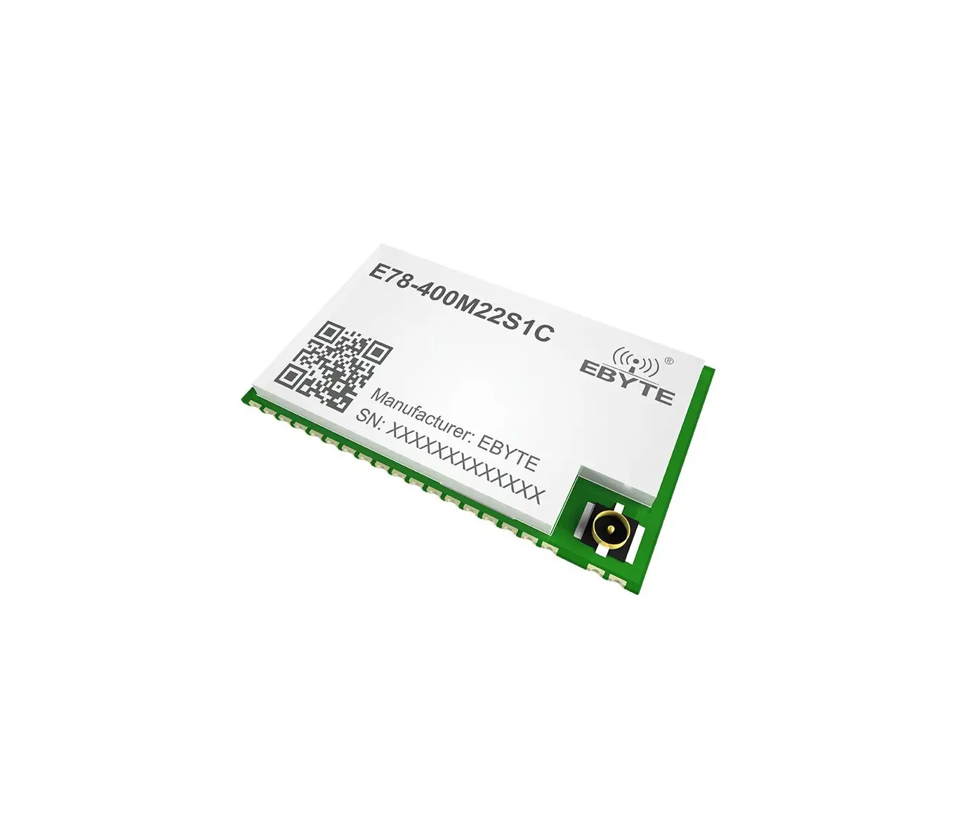
EBYTE E78-400M22S1C LPWAN Low Power LoRa Wireless SoC
Disclaimer
EBYTE reserves all rights to this document and the information contained herein.
Products, names, logos and designs described herein may in whole or in part be subject to intellectual property rights. Reproduction, use, modification or disclosure to third parties of this document or any part thereof without the express permission of EBYTE is strictly prohibited.
The information contained herein is provided “as is” and EBYTE assumes no liability for the use of the information. No warranty, either express or implied, is given, including but not limited, with respect to the accuracy, correctness, reliability and fitness for a particular purpose of the information. This document may be revised by EBYTE at any time. For most recent documents, visit www.ebyte.com.
Introduction
Brief Introduction
E78 series are RF transceiver module of various frequency bands designed and manufactured by Chengdu Ebyte, with long communication distance and extremely low power mode current consumption. It is a small-sized SMD type (pin pitch 1. lmm).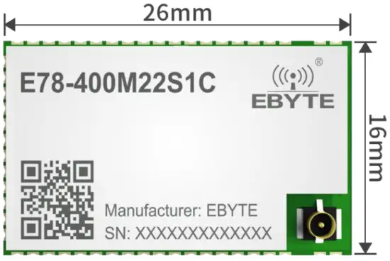
EBYTE E78-400M22S1C LPWAN Low Power LoRa Wireless SoC
Features
- The first domestic universal LPWAN wireless SoC module based on ASR6601SE;
- Support LoRaWAN, LinkWAN multiple protocol standards;
- Ultra-high sensitivity of -148 dBm and a maximum transmit power of 22 dBm;
- Support 42 configurable GPIOs3xI2C1xICS4xUART1xLPUART1xSWD3xSPI1xQSPI 2xWDG;
- 62.5Kbps air data rate under LoRa modulation, and 300Kbps under (G)FSK modulation;
- Support the global license-free ISM 433MHz band, support 470MHz meter reading frequency band;
- Support deep sleep, the power consumption of the whole machine is about 2uA in this mode;
- The measured communication distance can reach 5.5km;
- Built-in embedded LCD driver;
- Support AES, DES, RSA, ECC, SHA, SM2/3/4 hardware encryption;
- Industrial grade standard design, support -40 ~ 85 °C for working over a long time;
- IPEX and stamp hole optional, good for secondary development and integration.
Application
- Street lamp control, environmental monitoring, etc;
- Smart parking lot sensor;
- Smart home and industrial sensors, etc.
- Smart Agriculture Sensor;
- Wireless alarm security system;
- Building automation solutions;
- Wireless industrial-grade remote control;
- Health care products;
- Advanced Meter Reading Architecture(AMI).
Specification and parameter
Specification
| Model No. | Frequency | Transmit power | Reference distance(stamp hole/IPEX) | Package | Antenna |
| E78-400M22S1C | 410-490MHz | 21dBm | 5.5Km(Lora 1kbps) | SMD | Stamp/IPEX |
| Model No. | IC | Size | Net Weight | Operation Temperature | Operation Humidity | Storage Temperature |
| E78-400M22S1C | ASR6601S E | 26* 16*2.8 mm | 1.9g | -40 ~ 85℃ | 10% ~ 90% | -40 ~ 125°C |
Limit parameter
| Main parameter | Performance | Remark | |
| Min | Max | ||
| Power supply(V) | -0.3 | 3.9 | ≥3.9 V ensures output power |
| Digital input level voltage(V) | -0.3 | 3.9 | ≥3.9 V ensures output power |
| Rf input power(dBm) | – | +10 | Chances of burn is slim when modules are used in short distance |
| Temperature(℃) | Storage: -55~+125 | Operating: -40~+85 | Industrial grade |
| Humidity(%) | Storage: 5~95 | Operating: 10~95 | Without condensation |
Operating parameter
| Main parameter | Performance | Remark | ||
| Min | Type | Max | ||
| Power supply(V) | 1.7 | 3.3 | 3.7 | |
| Communication level(V) | 1.7 | 3.3 | 3.7 | |
| TX Current (mA) | 105 | 108 | 110 | LoRa Pout=+22dBm |
| RC current (mA) | 8.5 | 8.7 | 11 | LoRa 125KHz DCDC Mode, MCU Operation, Build-in TCXO |
| Sleep current(uA) | 0.8 | 1 | 1 | MCU reserved |
| Sleep current(uA) | 1.6 | 1.8 | 1.8 | RF/MCU/RTC reserved |
| TX power (dBm) | 20.6 | 20.8 | 21 | Set up Pout=+22dBm |
| Recommended frequency (MHz) | 410 | 433/470/490 | 490 | Module working frequency 410~490MHz |
| Receiving sensitivity (dBm) | – | -148 | – | |
| TCXO crystal (MHz) | – | 32 | – | Built-in crystal oscillator and uses PWR_TCXO for power supply |
| TCXO crystal voltage(V) | 1.8 | 1.8 | 3.3 | Recommended output voltage of PWR_TCXO pin |
| Antenna | IPEX/Stamp hole | 50 ohm impedance | ||
Parameter description
- When designing the power supply circuit for the module, it is recommended to reserve more than 30% of the remaining amount, and the whole machine is conducive to long-term stable operation;
- The current required for the inst ant of launch is large but often because the launch time is extremely short, the total energy consumed may be smaller;
- When customers uses an external antenna, the impedance matching degree between the antenna and the module at different frequency points will affect the magnitude of the transmission current to varying degrees;
- The current consumed by the RF chip in the pure receiving state is called the receiving current. Some RF chips with communication protocols or developers have loaded some self-developed protocols on the whole machine, which may cause the receiving current of the test to be too large;
- The current in the purely receiving state is often mA level, and the “receiving current” of the μA level needs to be processed by the developer through software;
- The shutdown current is often much smaller than the current consumed by the power supply part of the whole machine at no load, without being overly demanding;
- Since the material itself has a certain error, a single LRC component has an error of +0.1%. However, since a plurality of LRC components are used in the entire RF loop, there is a case where error accumulation occurs, resulting in a difference in emission current and reception current of different modules;
- Reducing the transmit power can reduce power consumption to some extent, but reducing the transmit power emissions for a number of reasons reduces the efficiency of the internal PA.
Size and pin definition
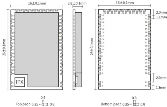
| Pin No. | Item | Direction | Description |
| 1 | GND | – | Ground wire, connected to the power reference ground |
| 2 | GND | – | Ground wire, connected to the power reference ground |
| 3 | GND | – | Ground wire, connected to the power reference ground |
| 4 | NC | – | Reserved |
| 5 | GPIO01 | Input/Output | MCU GPIO |
| 6 | GPIO00 | Input/Output | MCU GPIO |
| 7 | GPIO03 | Input/Output | MCU GPIO |
| 8 | GPIO02 | Input/Output | MCU GPIO |
| 9 | GPIO06 | Input/Output | MCU GPIO |
| 10 | GPIO07 | Input/Output | MCU GPIO |
| 11 | NRST | Input | External reset pin |
| 12 | GPIO14 | Input/Output | MCU GPIO |
| 13 | GPIO15 | Input/Output | MCU GPIO |
| 14 | GPIO23 | Input/Output | MCU GPIO |
| 15 | GPIO25 | Input/Output | MCU GPIO |
| 16 | GPIO24 | Input/Output | MCU GPIO |
| 17 | GPIO27 | Input/Output | MCU GPIO |
| 18 | GPIO26 | Input/Output | MCU GPIO |
| 19 | GPIO29 | Input/Output | MCU GPIO |
| 20 | GND | – | Ground wire, connected to the power reference ground |
| 21 | GPIO28 | Input/Output | MCU GPIO |
| 22 | GPIO30 | Input/Output | MCU GPIO |
| 23 | GPIO31 | Input/Output | MCU GPIO |
| 24 | GPIO62 | Input/Output | MCU GPIO |
| 25 | UART0_RX | Input | MCU GPIO |
| 26 | UART0_TX | Output | MCU GPIO |
| 27 | GPIO60 | Input/Output | MCU GPIO |
| 28 | GPIO58 | Input/Output | MCU GPIO |
| 29 | GPIO13 | Input/Output | MCU GPIO |
| 30 | GPIO12 | Input/Output | MCU GPIO |
| 31 | VCC | – | Power supply, range 2.5V ~ 3.7V (recommended to add external ceramic filter capacitor) |
| 32 | GND | – | Ground wire, connected to the power reference ground |
| 33 | GND | – | Ground wire, connected to the power reference ground |
| 34 | GPIO11 | Input/Output | MCU GPIO |
| 35 | GPIO08 | Input/Output | MCU GPIO |
| 36 | GPIO05 | Input/Output | MCU GPIO |
| 37 | GPIO04 | Input/Output | MCU GPIO |
| 38 | GPIO09 | Input/Output | MCU GPIO |
| 39 | GPIO45 | Input/Output | MCU GPIO |
| 40 | GPIO44 | Input/Output | MCU GPIO |
| 41 | GPIO42 | Input/Output | MCU GPIO |
| 42 | GPIO41 | Input/Output | MCU GPIO |
| 43 | GPIO40 | Input/Output | MCU GPIO |
| 44 | GPIO37 | Input/Output | MCU GPIO |
| 45 | GPIO33 | Input/Output | MCU GPIO |
| 46 | GPIO32 | Input/Output | MCU GPIO |
| 47 | GPIO36 | Input/Output | MCU GPIO |
| 48 | GPIO35 | Input/Output | MCU GPIO |
| 49 | GPIO34 | Input/Output | MCU GPIO |
| 50 | GND | – | Ground wire, connected to the power reference ground |
| 51 | ANT | Output | Antenna interface, stamp hole (50 ohm characteristic impedance) |
| 52 | GND | – | Ground wire, connected to the power reference ground |
| ★ For the pin definition,software driver and communication protocol of the module, please refer to ASR official 《ASR6601SE Datasheet》 ★ | |||
E78-400M22S1C development
- In the process of software development, please be sure to follow ASR6601SE official user manual and related software development materials in detail, details see ASR official;
- The E78-400M22S1C module has a built-in 32MHz TCXO. The crystal power supply uses the PWR_TCXO pin ofthe ASR6601SE chip. The recommended voltage is 1.8V;
- The module has a built-in external 32.768KHz crystal oscillator, and the load capacitance of the crystal oscillator is programmable inside the ASR6601SE chip
- Module firmware download can use SWD and UART two ways, the pins are respectively.
Download port Pin description SWD GPIO06 (SWDATA), GPIO07 (SWCLK), NRST respectively are the 9th, 10th, and 11th pins Serial UART0_RX and UART0_TX respectively are the 25th and 26th pins Note: Use the official SDK, before starting to download, please connect GPIO02 to high level, then restart the module to enter the serial download mode. - The module integrates a radio frequency switch, which supports two modes of single control and dual control, see the table below for details:
Operating mode GPIO10 GPIO59 Remark Transmit mode 1 1 Single control mode Receive mode 1 0 Single control mode Others: GPIO59 (LORA_RF_SWITCH) is the DIO2 pin with built-in RF. After the official SDK is modified to TCXO mode, it can be directly downloaded to the module for running test.
FAQ
Communication range is too short
- The communication distance will be affected when obstacle exists;
- Data lose rate will be affected by temperature, humidity and co-channel interference;
- The ground will absorb and reflect wireless radio wave, so the performance will be poor when testing near ground;
- Sea water has great ability in absorbing wireless radio wave, so performance will be poor when testing near the sea;
- The signal will be affected when the antenna is near metal object or put in a metal case;
- Power register was set incorrectly, air data rate is set as too high (the higher the air data rate, the shorter the distance);
- The power supply low voltage under room temperature is lower than 2.5V, the lower the voltage, the lower the transmitting power;
- Due to antenna quality or poor matching between antenna and module.
Module is easy to damage
- Please check the power supply, ensure it is between the recommended values, voltage exceed the maximum thanwill cause permanent damage to the module.
- Please check the stability of power supply, the voltage cannot fluctuate too much.
- Please make sure antistatic measure are taken when installing and using, high frequency devices have electrostatic susceptibility.
- Please ensure the humidity is within limited range, some parts are sensitive to humidity.
- Please avoid using modules under too high or too low temperature.
Production guidance
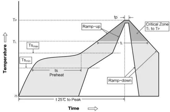
Reflow soldering temperature
| Profile Feature | Curve characteristics | Sn-Pb Assembly | Pb-Free Assembly |
| Solder Paste | Solder paste | Sn63/Pb37 | Sn96.5/Ag3/Cu0.5 |
| Preheat Temperature min (Tsmin) | Min preheating temp. | 100℃ | 150℃ |
| Preheat temperature max (Tsmax) | Mx preheating temp. | 150℃ | 200℃ |
| Preheat Time (Tsmin to Tsmax)(ts) | Preheating time | 60-120 sec | 60-120 sec |
| Average ramp-up rate(Tsmax to Tp) | Average ramp-up rate | 3℃/second max | 3℃/second max |
| Liquidous Temperature (TL) | Liquid phase temp. | 183℃ | 217℃ |
| Time(TL)Maintained Above(TL) | Time below liquid phase line | 60-90 sec | 30-90 sec |
| Peak temperature(Tp) | Peak temp. | 220-235℃ | 230-250℃ |
| Aveage ramp-down rate(Tp to Tsmax) | Aveage ramp-down rate | 6℃/second max | 6℃/second max |
| Time 25℃ to peak temperature | Time to peak temperature for 25℃ | 6 minutes max | 8 minutes max |
Reflow soldering curve
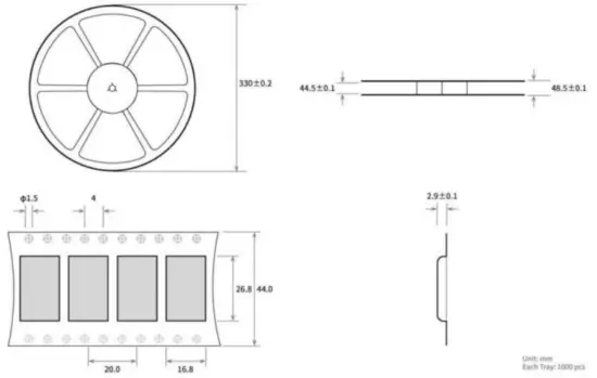
Bulk packaging
Revision history
| Version | Date | Description | Issued by |
| 1.0 | 2020/12/01 | Initial version | Linsoin |
About us
Technical support: [email protected]
Documents and RF Setting download link: www.ebyte.com
Thank you for using Ebyte products! Please contact us with any questions or suggestions: [email protected]
————————————————————————————————-
Phone: +86 028-61399028
Web: www.ebyte.com
Address: B5 Mould Park, 199# Xiqu Ave, High-tech District, Sichuan, China
![]() Chengdu Ebyte Electronic Technology Co.,Ltd. 11
Chengdu Ebyte Electronic Technology Co.,Ltd. 11