![]()
User Manual
DA16600 Evaluation Kit
UM-WI-026
Abstract
This document describes how to set-up and use the DA16600 Evaluation Kit.
Terms and Definitions
| DPM AP USB UART RTC WPS SSID SDK ARP | Dynamic Power Management Access Point Universal Serial Bus Universal Asynchronous Receiver-Transmitter Real Time Clock Wi-Fi Protected Setup Service Set Identifier Software Development Kit Address Resolution Protocol |
References
[1] DA16200, Datasheet, Dialog Semiconductor
[2] UM-WI-002, DA16200, SDK Programmer Guide, User Manual, Dialog Semiconductor
[3] UM-WI-023, DA16200, EVK User Manual, Dialog Semiconductor
[4] UM-B-114, DA14531, Devkit Pro Hardware, User Manual, Dialog Semiconductor
DA16600 Module EVK
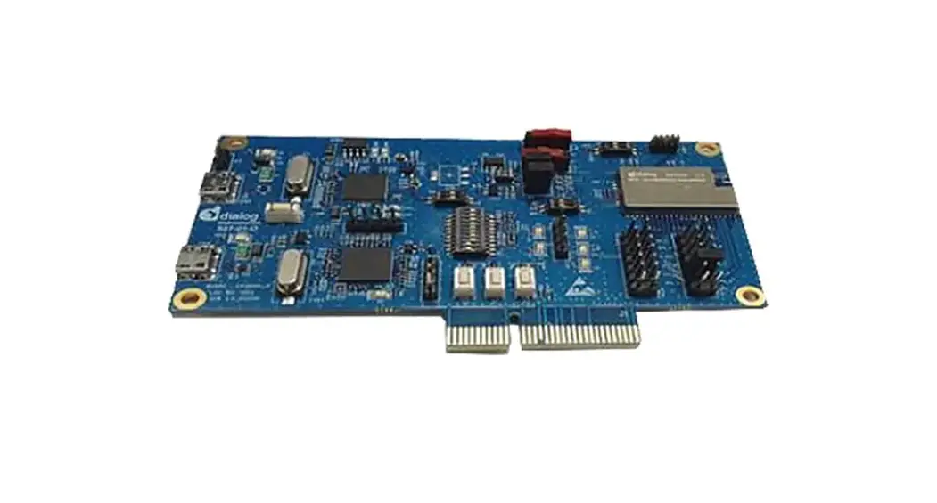
Figure 1 shows the hardware configuration of the DA16600 Module Evaluation Kit (EVK).
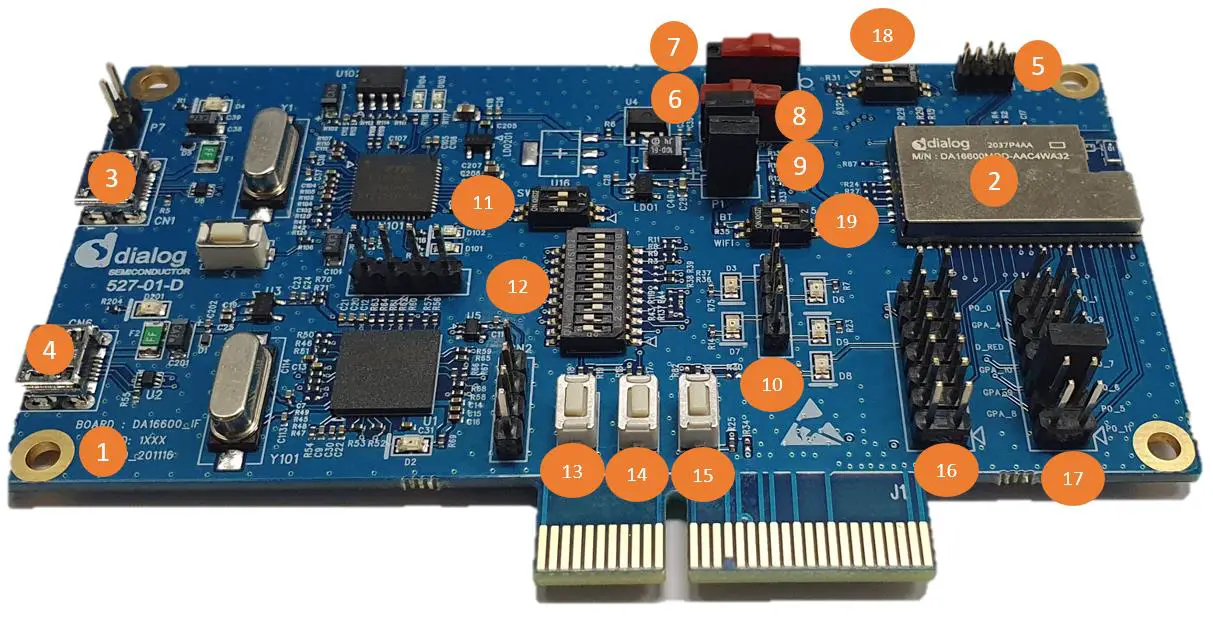
Figure 1: Hardware Configuration
DA16600 EVB has the following components:
- Main board: DA16600 module (DA16600MOD-AAC) is installed.
- DA16600MOD-AAC Wi-Fi & Bluetooth® LE Combo Module.
- USB Port: UART0 is for debug, UART1 is for test.
- USB Port: to debug, connect directly to DA14531, but do not use this port for normal operation.
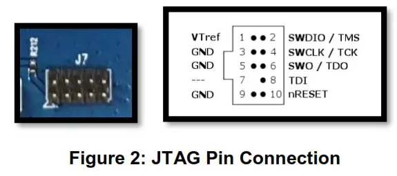
- JTAG PIN: allows connecting to I-jet (a JTAG debugger from IAR). See Figure 2.
• Pin 7 is keyed with a white plug, so Pin 7 should be removed on EVK
- RTC Wake up2 key: a switch to wake up the board from Sleep Mode.
- RTC Power key: a switch to turn On/Off the board.
- Pin (P2): a jumper to measure current at Wi-Fi part. For normal operation, this pin should be shorted.
• Pull out the Short Pin cap and connect the jumper wire to measuring equipment - Pin (P1): a jumper to measure current at Bluetooth® LE part. For normal operation, this pin should be shorted.
• Pull out the Short Pin cap and connect the jumper wire to measuring equipment - Connector CN4: GPIO test purpose connector.
To test GPIO in J2 and J14, connect to LED by this connector. - Switch SW3: a switch to connect directly to DA14531 and use UART to check Bluetooth® LE performance.
This switch is set to Off in normal operation - Switch SW7: a multipurpose switch.
This switch is set to Off in normal operation - Switch S2: factory reset button using GPIOA7.
Set to ON at Pin2 of SW7 to use this switch - Switch S1: WPS button using GPIOA6.
Set to ON at Pin1 of SW7 to use this switch - Switch S3: reset button of DA14531 in test mode.
- Connector J2: GPIO connector.
- Connector J14: GPIO connector.
- Switch SW4: a switch to control RF switch in DA16600MOD at test mode.
- Switch SW5: a switch to check current consumption using power meter kit.
Description of Switch
Turn On Case of SW7
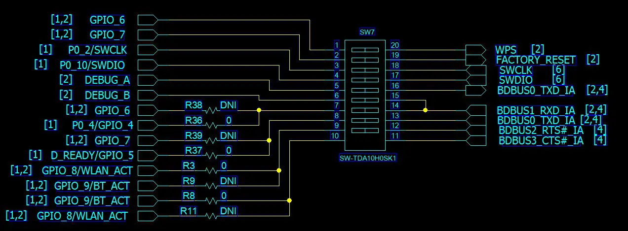
- Pin1: When using the WPS function by GPIOA_6, turn on this pin to connect S1.
- Pin2: When using the Factory reset function using GPIOA_7, turn on this pin to connect S2.
- Pin3,4: When Debugging DA14531 by Keil.
- Pin5,6: When check debug message of DA14531 in example application.
- Pin7,8: When using UART1 of DA16200 by GPIOA_4,5.
Turn On Case of SW3
Turn On Case of SW4

When manually controlling the internal RF switch of DA16600.
- Pin1: When RF path is connected to DA14531( Bluetooth® LE).
- Pin2: When RF path is connected to DA16200( Wi-Fi).
Turn On Case of SW5

When measure the current consumption using power meter kit.
- Pin1: When measure current consumption of DA16200 ( Wi-Fi) which include RF switch.
- Pin2: When measure current consumption of DA14531 ( Bluetooth® LE).
Wi-Fi Provisioning Setup
DA16600 Connecting the Board
This section describes the installation procedure for the drivers, the configuration of the serial port, and the steps needed to verify the connection with the PC as well as solutions to problems that may occur.On first connection to a host PC running Microsoft Windows, the system detects several devices and automatically installs all necessary drivers. If drivers are not automatically installed, you can get them from the following url: http://www.ftdichip.com/Drivers/CDM/CDM21224_Setup.zip. The Windows driver creates two virtual COM ports. The first COM port (lower number, COM35 in this example) provides a UART interface for debugging or firmware download between the PC and the DA16600. See Figure 3.
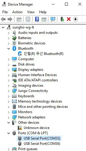
Figure 3: Check COM Ports on Device Manager
Configure the Serial Port for UART
For a Windows Host, the Tera Term utility is used to fully validate the connection to the DA16600 EVK.
Tera Term is a free software terminal emulator (communication program) which supports multiple communication including Serial port connections. Download Tera Term from https://ttssh2.osdn.jp. Run the teraterm-x.yy.exe and follow the installation wizard.
To make sure that the communication between the DA16600 EVK and host PC is properly established, you need to verify the UART connection between the two nodes. Do the following:
- Connect the DA16600 EVK to the PC to USB Port via USB cable.
- Verify that the host identifies two serial ports as shown in Figure 3 the second is connected to UART (see Section 4.1).
- In the Windows Start menu, open Tera Term.
- In the Tera Term: New connection dialog, do the following:
a. Select Serial.
b. Select the COM Port to use.
c. Click OK. - Select Setup > Serial Port and configure your UART port using the parameters as shown in Figure 4.
- Open the Lowest COM port number assigned to the DA16600 EVK. Figure 3 shows which port number to select in Device Manager in Windows. Make sure that the UART is configured as shown in Figure 4.
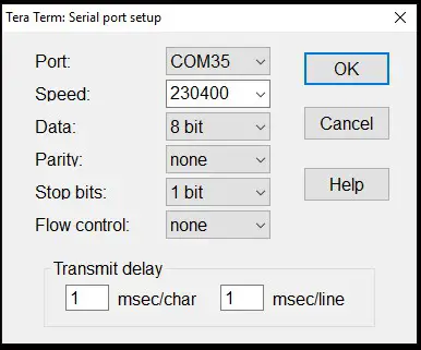 Figure 4: Serial Port Setup
Setup for Wi-Fi Provisioning Using Bluetooth® LE
DA16600 module may be used in a product like “Wi-Fi door-lock” where Wi-Fi is playing the main role, and Bluetooth® LE assists with Wi-Fi Provisioning at the product’s initial setup (Out-of-Box). A Bluetooth® LE peer application (for example Android/IOS mobile App) interacts with users to set up DA16600 device – by giving Wi-Fi Provisioning information (for example Wi-Fi Home router’s SSID, password, server info, and other).
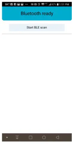
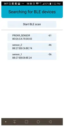
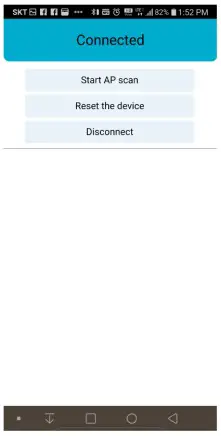
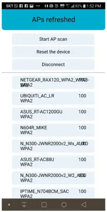
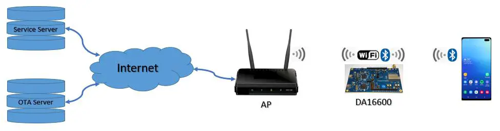 Figure 5: Diagram of Provisioning via Bluetooth® LE To set up Wi-Fi provisioning:
- Check the prompt [/DA16200] #.
- Run Provisioning App and follow the steps in Table 1.
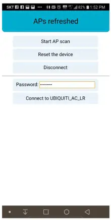
Table 1: Steps for Provisioning via Bluetooth® LE
| 1. Start App to scan Bluetooth® LE | 2. Select DA16600 to connect App to DA16600. | 3. Press Start AP Scan button to find AP. |
 |  |  |
| 4. Choose application you want | 5. Enter password for the | 6. Wi-Fi provisioning is completed. |
 |  |  |
Current Measurement
For detailed information on Sleep mode, see the Low Power Operation Mode section in DA16200 Datasheet [1]. To measure current waveform, connect EVK’s current measurement point (P1 and P2) with the measurement instrument (KEYSIGHT 14585A).
Figure 6 shows a typical test setup environment.
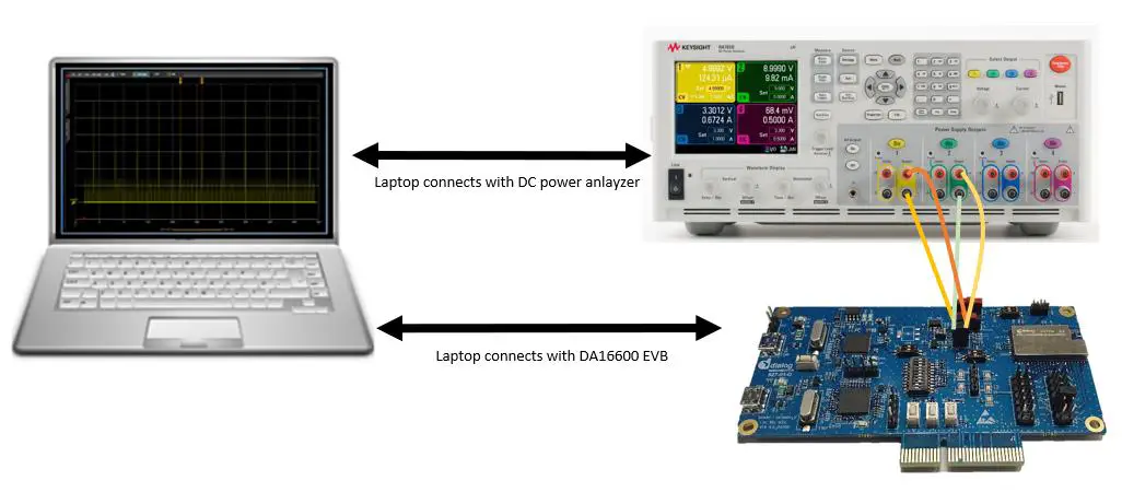
Figure 6: Current Test Environment
For more detailed information on using power meter kit, see
DA16600_SB_Power_Meter_Kit_User_Manual [1].
Hardware Setup for RF Test
DA16600MOD consists of DA16200 and DA14531 chipsets, see chipset GUI guides for details:
[1] UM-WI- 004_DA16200_AT_GUI_Tool_User_Manual_Rev_1v3
[2] AN-B-077 DA14531 Bluetooth Direct Test Mode v1.0
Wi-Fi Test Setup
GPIOA4 and GPIOA5 can be used with UART to test RF performance of DA16200. Turn on pin 7 and 8 of SW7 to use UART with GPIOA4 and GPIOA5.
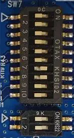
Figure 7: SW3 and SW7 Set to Use AT-GUI
Bluetooth® LE Test Setup
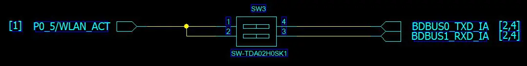
P0_5 can be used with 1-wire UART to test RF performance of DA14531. Turn on pin1 and 2 of SW3 to use UART and turn off pin 7 and 8 of SW7.
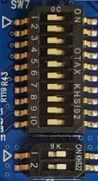
Figure 8: SW3 and SW7 Set to Use SmartSnippets
SW4 can control RF switch. Turn on pin1 of SW4 to control RF switch to Bluetooth® LE RF path.
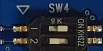 Figure 9: SW4 Set to Use Bluetooth® LE RF Path
Firmware Update
The security features of DA16600 support Secure Boot to avoid booting with fake or untrusted images and to protect against hacking. The DA16200 SoC includes a security hardware block called CryptoCell-312 (CC312). With proper security keys and certificates installed (in OTP and images), the DA16200 can boot in secure mode.
DA16600 requires four images. With a serial terminal tool, each image can be loaded individually:
- <Bootloader image>: also known as Second Bootloader
- DA16200_[image_type]-[vendor]-[major]-[minior]-
[customer_ver]_[sflash_model].img- [Image_type]: Bootloader (BOOT), Main, or System library (SLIB)
- [vendor]: Internal use by vendor
- [major]: Major version
- [minor]: Minor version or SDK patch version
- [customer_ver]: User-configurable customer version
- [sflash_model]: sflash model or type used
- For example: DA16200_BOOT-GEN01-01-xxxxx-xxxxxx_W25Q32JW.img
- DA16200_[image_type]-[vendor]-[major]-[minior]-
- <System Library image>: includes RF drivers and libraries for DPM
- For example: DA16200_SLIB-GEN01-01-xxxxx-xxxxxx.img
- <Main image>: includes RTOS and applications
- For example: DA16200_RTOS-GEN01-01-xxxxx-xxxxxx.img
- <DA14531 image>:
- For example: DA14531_multi_part_proxr_peri.img
Flash MAP
DA16200 provides two images: #0 and #1. You can use these regions for each image set and change the index of the booting image set. The default value of the Boot Index is #0.
Table 2: 4 MB Serial Flash Memory Map
| Address | Item | Size |
| 0x0000_0000 | 2nd Bootloader | 36 kB |
| 0x0000_9000 | Boot Index | 4 kB |
| 0x0000_A000 | RTOS #0 | 1536 kB |
| 0x0018_A000 | SLIB #0 (RamLib + TIM) | 64 kB |
| 0x0019_A000 | User Area #0 | 364 kB |
| 0x0020_0000 | RTOS #1 | 1536 kB |
| 0x0038_0000 | SLIB #1 (RamLib + TIM) | 64 kB |
| 0x0039_A000 | User Area #01 | 448 kB |
Bootloader Image
<Bootloader image> is also known as the second bootloader and is the first thing loaded into memory for a factory-created DUT (for example with an empty flash). Note that this image has SFDP information, which is important sflash type information, so always load this image before loading other images.
If you get a new SDK, then you should start with loading the <Bootloader image>. To load the <Bootloader image>:
- Turn on the DA16600 board.
- At the [/DA16200] prompt, type reset to go to the Mask ROM prompt [MROM]. See Figure 10.
 Figure 10: Mask ROM
 - At the [MROM] prompt, type loady boot. See Figure 11.
 Figure 11: Bootloader Prompt on Command Window
 - Choose menu File > Transfer > YMODEM > Send to select the image file for the Bootloader. See Figure 12.
• For example: DA16200_BOOT-GEN01-01-xxxxx-xxxxxx_W25Q32JW.img
• The result is printed at the end of the transfer. Please ignore any messages like “err:..”
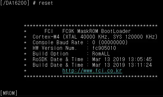 Figure 10: Mask ROM
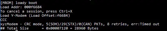 Figure 11: Bootloader Prompt on Command Window
Figure 12: Load Image File
System Library Image
The <System Library image> includes system libraries, RF drivers, and libraries to operate the DPM. To load the <System Library image>:
- At the [MROM] prompt, type loady 18a000 to load a <System Library image> in boot index #0. See Figure 13.
 Figure 13: System Library Prompt on Command Window
 - Choose menu File > Transfer > YMODEM > Send to select the <System Library image> file. See Figure 14.
• For example: DA16200_SLIB-GEN01-xx-xxxxx-xxxxxx.img
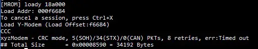 Figure 13: System Library Prompt on Command Window
Figure 14: Load Image File
Main RTOS Image
This <Main image> contains RTOS, Wi-Fi libraries, and system/user applications. To load the <Main image>:
- At the [MROM] prompt, type loady a000. See Figure 15.
 Figure 15: Main Image Prompt on Command Window
 - Choose menu File > Transfer > YMODEM > Send to select the <Main image> file. See Figure 16.
• For example: DA16200_RTOS_GEN01-XX-YYYY-ZZZZZZ.img
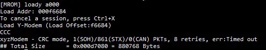 Figure 15: Main Image Prompt on Command Window
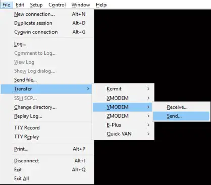 Figure 16: Load Image File
DA14531 Image
This <DA14531 image> is downloaded to DA14531 during booting sequence. To load <DA14531 image>:
- At the [MROM] prompt, type loady 392000 1000 bin. See Figure 17
 Figure 17: DA14531 Image Prompt on Command Window
 - Choose menu File > Transfer > YMODEM > Send to select the <Main image> file.
• For example: da14531_multi_part_proxr_peri.img Figure 18: Load Image File
 - If the four images are loaded, then at the[MROM] prompt, type boot to boot your images.
- Run factory reset as shown in Figure 19.
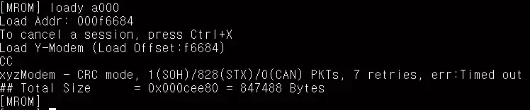 Figure 17: DA14531 Image Prompt on Command Window
 Figure 18: Load Image File
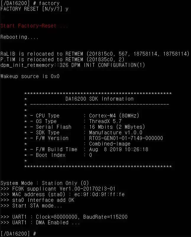
Figure 19: Factory Mode Prompt on Command Window
NOTE
Now all four required images are loaded.
Serial Flash Recovery
When the serial flash is replaced, the flash memory map is changed, or if you think that the flash memory is corrupted, then do the following to re-initialize or recover sflash and check the process:
- Boot DA16200.
- At the [/DA16200] # prompt, run reset command.
- At [MROM] prompt, run sflash info command to read serial flash information.
For example, SFLASH: ef601615. This is the flash product ID of W25Q32JW. See also the IDs below.
W25Q32JWSNIQ: ef601615 - Run ymodem sfdp command.
- In the buildSBOOTSFDP folder, find Flash SFDP file which is corresponding to Flash ID as W25Q32JW.bin.
- Run sflash erase 0 400000 command [MROM] to erase the entire flash for recovery.
Note that this command can take a long time to complete. Wait until the [MROM] prompt appears again. - Re-load all images in the specified order for serial flash recovery.
a. [MROM] loady boot.
b. [MROM] loady 18a000.
c. [MROM] loady a000.
d. [MROM] loady 392000 1000 bin. - Run boot command to boot DA16600. The image version is printed.
- Initialize NVRAM for Serial Flash Recovery with following commands:
[/DA16200] # nvram
[/DA16200/NVRAM] # nvedit erase sflash
[/DA16200/NVRAM] # nvedit clear
[/DA16200/NVRAM] # nvcfg update flash update , sflash completed
[/DA16200/NVRAM] # nvedit load flash nvedit , load completed
[/DA16200/NVRAM] #
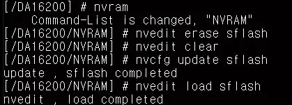
Figure 20: Initialize NVRAM
Serial Flash Recovery from Boot
If there are any memory conflicts during updating the image or errors while building the SDK, the reason might be that it cannot run DA16200. In this case, you cannot do anything in the command window. DA16200 must be forced to enter boot mode. Do the following:
- Use RTC_PWR_KEY to turn off (move to OFF position).
• Connect two pins: Pin 11(F_CLK) and P12(GND) of J2. See Figure 21 Figure 21: Recovery Point in the EVK
 - Use RTC_PWR_KEY to turn on (move to ON position).
a. Turn on RTC_PWR_KEY to boot DA16600.
b. Disconnect the two pins of J2. Pin 11 (F_CLK) and Pin 12 (GND).
The DA16600 go into the BOOT mode. See Figure 22. - At the [BOOT] # prompt, run reset command.
- Do the steps in Section 7.6 from step 3.
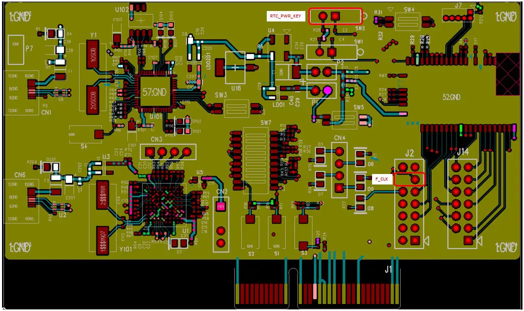 Figure 21: Recovery Point in the EVK
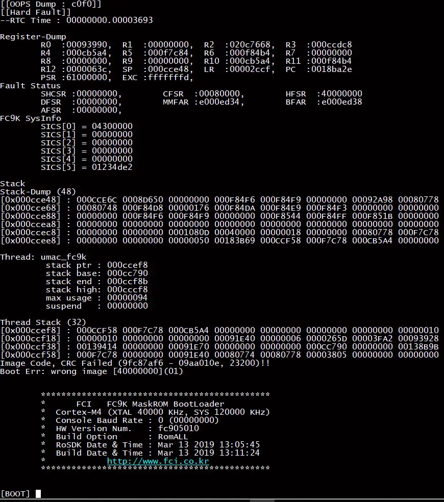
Figure 22: Run with BOOT Mode
Revision History
| Revision | Date | Description |
| 1.1 | 20-Jan-21 | Change board picture and add description of switch |
| 1.0 | 30-Jul-20 | Initial Version |
Status Definitions
| Status | Definition |
| DRAFT | The content of this document is under review and subject to formal approval, which may result in modifications or additions. |
| APPROVED or unmarked | The content of this document has been approved for publication. |
Disclaimer
Unless otherwise agreed in writing, the Dialog Semiconductor products (and any associated software) referred to in this document are not designed, authorized or warranted to be suitable for use in life support, life-critical or safety-critical systems or equipment, nor in applications where failure or malfunction of a Dialog Semiconductor product (or associated software) can reasonably be expected to result in personal injury, death or severe property or environmental damage. Dialog Semiconductor and its suppliers accept no liability for inclusion and/or use of Dialog Semiconductor products (and any associated software) in such equipment or applications and therefore such inclusion and/or use is at the customer’s own risk.
Information in this document is believed to be accurate and reliable. However, Dialog Semiconductor does not give any representations or warranties, express or implied, as to the accuracy or completeness of such information. Dialog Semiconductor furthermore takes no responsibility whatsoever for the content in this document if provided by any information source outside of Dialog Semiconductor.
Dialog Semiconductor reserves the right to change without notice the information published in this document, including, without limitation, the specification and the design of the related semiconductor products, software and applications. Notwithstanding the foregoing, for any automotive grade version of the device, Dialog Semiconductor reserves the right to change the information published in this document, including, without limitation, the specification and the design of the related semiconductor products, software and applications, in accordance with its standard automotive change notification process.
Applications, software, and semiconductor products described in this document are for illustrative purposes only. Dialog Semiconductor makes no representation or warranty that such applications, software and semiconductor products will be suitable for the specified use without further testing or modification. Unless otherwise agreed in writing, such testing or modification is the sole responsibility of the customer and Dialog Semiconductor excludes all liability in this respect.
Nothing in this document may be construed as a license for customer to use the Dialog Semiconductor products, software and applications referred to in this document. Such license must be separately sought by customer with Dialog Semiconductor.
All use of Dialog Semiconductor products, software and applications referred to in this document is subject to Dialog Semiconductor’s Standard Terms and Conditions of Sale, available on the company website (www.dialog-semiconductor.com) unless otherwise stated.
Dialog, Dialog Semiconductor and the Dialog logo are trademarks of Dialog Semiconductor Plc or its subsidiaries. All other product or service names and marks are the property of their respective owners.
© 2021 Dialog Semiconductor. All rights reserved.
Contacting Dialog Semiconductor
United Kingdom (Headquarters)
Dialog Semiconductor (UK) LTD
Phone: +44 1793 757700
Email: [email protected]
Web site: www.dialog-semiconductor.com


