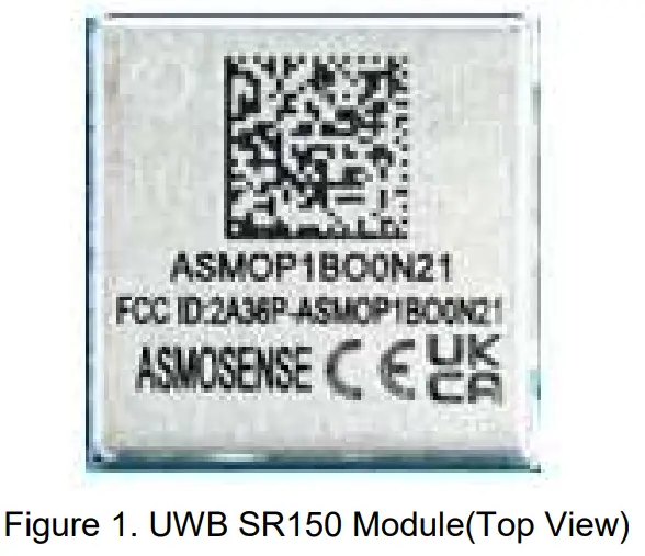
AMO ASMOP1BO0N21 UWB SR150 Module
Main features
- Supports SHF UWB bands from 6.24 GHz to 8.24 GHz for worldwide use
- The programmable transmitter output power of up to +9dBm
- Data rates of 110 kbps, 850 kbps, 6.8 Mbps, 7.8 Mbps
- Supports 2-way ranging and TDOA measurement
- Supports Angle of Arrival (AoA) Measurement
- ARM® Cortex-M33 32-bit Processor
- Embedded PHY and MAC compatible with FiRa consortium specification
- One I2C Interface – interface to Secure Element (SE)
- One SPI Interface
- Up to 3 GPIOs
- Up to 4 timing-critical GPOs for T/R and antenna switching
- Single Typ. 1.8V supply
- Module size : 10mm x 10 mm x 1.8mm
Module Block Diagram
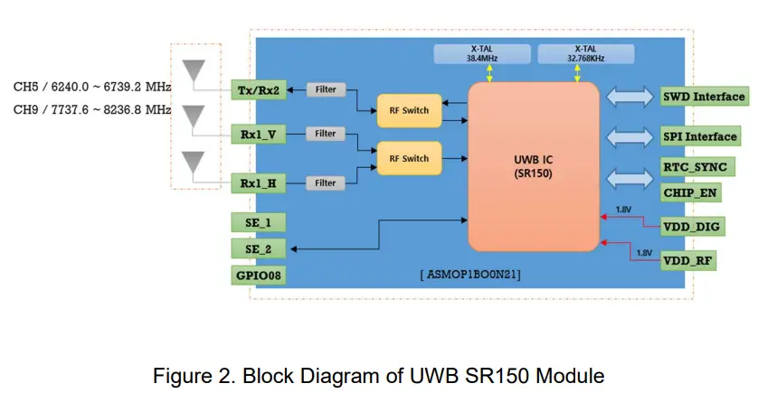
UWB SR150 Module Pin Diagram
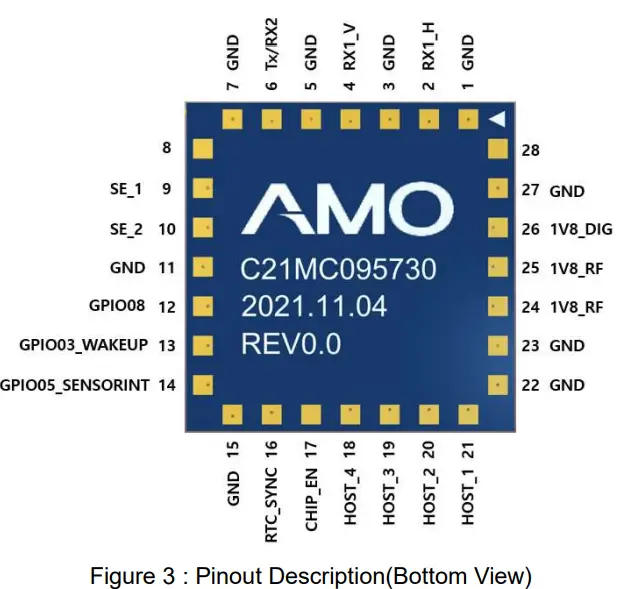
| PIN | PIN Name | PIN Type | Description |
| P1 | GND | G | Ground supply |
| P2 | RX1_H | I | RX1_Horizontal IN |
| P3 | GND | G | Ground supply |
| P4 | RX1_V | I | RX1_Vertical IN |
| P5 | GND | G | Ground supply |
| P6 | TX/RX2 | I/O | TX OUT / RX2 In |
| P7 | GND | G | Ground supply |
| P8 | – | – | – |
| P9 | SE_1 | I/O | clock for the secure element I2C interface |
| P10 | SE_2 | I/O | SDA connection for secure element I2C interface |
| P11 | GND | G | Ground supply |
| P12 | GPIO8 | I/O | SE_IRQ. GPIO8 |
| P13 | GPIO03_WAKEUP | I/O | Host wakeup |
| P14 | GPIO05_SENSORINT | I/O | GPIO05 |
| P15 | GND | G | Ground supply |
| P16 | RTC_SYNC | I | Real Time Clock Synchronization |
| P17 | CHIP EN | I/O | connection for disabling/ enabling the chip |
| P18 | HOST_4 | I/O | MISO connection for the SPI host interface |
| P19 | HOST_3 | I/O | MOSI connection for the SPI host interface |
| P20 | HOST_2 | I/O | Slave select connection for the SPI host interface |
| P21 | HOST_1 | I/O | clock for the SPI host interface |
| P22 | GND | G | Ground supply |
| P23 | GND | G | Ground supply |
| P24 | VDD_1.8V_RF | P | 1.8V Power supply for RF |
| P25 | VDD_1.8V_RF | P | 1.8V Power supply for RF |
| P26 | VDD_1.8V_DIG | P | 1.8V Power supply for Digital |
| P27 | GND | G | Ground supply |
| P28 | – | – | – |
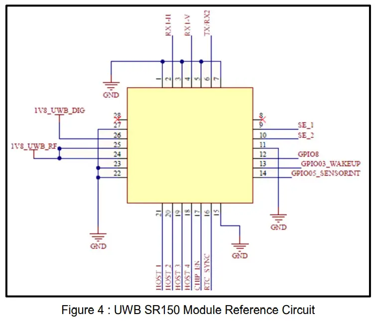
Reference Circuit
Module Characteristics
Electrical Characteristics
| Parameter | Min | Typ. | Max | Unit |
| Supply Voltage(VDD) | 1.71 | 1.8 | 1.98 | V |
| SR150 Current Consumption – Hard Power Down State – Peak Current RX(Dual RX) | – | – | 5 306 | uA mA |
| – Peak Current TX(Max) | 273 | mA | ||
| Operating Temperature | -30 | 25 | +85 | ˚c |
| RF Input Power | – | – | 7 | dBm |
| ESD (Human Body Model) | 2000 | V |
RF Characteristics
- T = 25°C, VDD = 3.3 V (typ.)
Parameter Condition Min Typ. Max Unit Frequency Range 6.24 – 8.24 GHz TX Output Power CW 12 dBm CH5 during preamble peak 9.5 CH9 during preamble peak 10.5 Data Rate 0.85 6.8 31.2 Mbps AOA accuracy SNR ≥ 34dB at input -3 +3 Deg 26dB ≤ SNR < 36dB at input
-10 +10 ToF accuracy LOS when STS is used -10 +10 Cm NLOS when STS is used -20 +20 RF Sensitivity Single / 6.8 Mbps -92 dBm Dual / 6.8 Mbps -94
Power Up
UWB SR150 Module needs several external power supplies to work.
| Parameter | Min | Typ. | Max | Unit |
| Supply Voltage(VDD) | 1.71 | 1.8 | 1.98 | V |
SR150 Module has a main power up sequence that require VDD. High level boot sequence is indicated below, when voltages are settled down CE can be asserted along with VDD within 50us, else design will transition to HPD state.
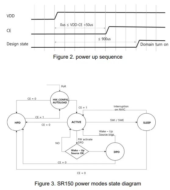
SYSTEM MODES
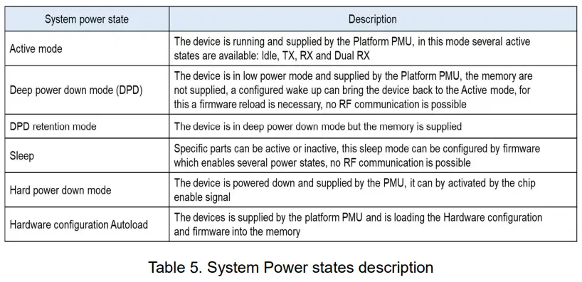
The SR150 Module has 6 power modes that are specified: Host power down mode, Deep power down mode, Deep power down retention mode, Sleep, Active mode and Hardware configuration Autoload. A description of the states can be found in Table 4
The time required for SR150 to go into DPD from is <100us controlled by the firmware. Similarly, the required time for SR150 to enter HPD state is less than 100us starting for the instance that CE is de-asserted. The Wakeup timing from DPD state is around 370 us, the wakeup form HPD state is triggered once CE is asserted and takes around 380us.
Host interface (SPI)
SPI-bus Master/Slave interface, up to 20 Mbits/s
Features
- Synchronous, Serial, Full-Duplex communication, up to 16.66 Mbits/s
- Data frames of 8-bits and 16bits supported
- Programmable clock polarity and phase
- LSB/MSB first order
- Programmable SSEL polarity
SPI-bus configuration options In order to select SPI-bus interface for host communication, the host interface choice and settings are programmed during production. The SPI-bus IP supports four operating modes selectable using SPInCfg register. The operation mode of the SPI-bus is shown in Table 5, CPHA refers to the Clock Phase option and CPOL refers to the Clock Polarity.
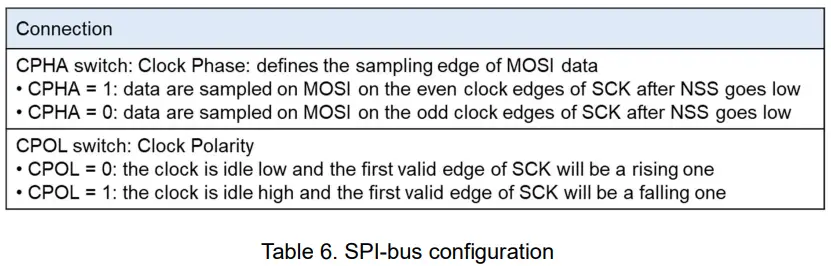
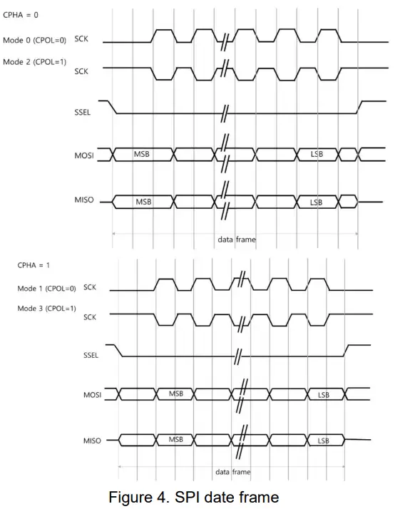
The SPI-bus interface shares the pins with the other host interfaces that are supported by SR150. When SPI-bus is configured the functionality of the interface pins is as described in Table 6. When a master device transmits data to the SR150 via the MOSI line, the SR150 responds by sending data to the master device via the MISO line. This implies fullduplex transmission with both, data out and data in synchronized with the same clock signal. SR150 starts sampling when receiving a logic low at pins NSS Host_2 pin and the clock at input pin HOST_1. Thus, SR150 is synchronized with the master. Data from the master is received serially at the slave MOSI line and loaded in the 8-bit shift register. After the 8bit shrift register is loaded, its data is transferred to the read buffer. During a write cycle, data is written into the shift register, then the SR150 waits for a clock train form the master to shift the data out on the MISO line. Both master and slave devices must operate with the same timing. The master device always places data on the MOSI line a half cycle before the clock edge SCK, for the slave device to latch the data.
These connections are used for communication between host and SR150 via SPI bus.
| Pin | functionality | HW connection when used | HW connection when NOT used |
| Host conntection | |||
| Host_1 | SCK (Serial input Clock) | host | Must be connected |
| Host_2 | NSS (Not Slave Select) | host | Must be connected |
| Host_3 | MOSI (Master Out Slave In) Data input | host | Must be connected |
| Host_4 | MISO (Master In Slave Out) Data output | host | Must be connected |
| GPIO05_SENSORINT | IRQ sent to the Host to let it know data are available for read | host | Must be connected |
| CHIP_EN | connection for the HOST to disable/enable the chip | host | Must be connected |
| RTC_SYNC | TBD | TBD | TBD |
| GPIO03_WAKEUP | SPI Rx Handshake from Host to SR150 | host | Must be connected |
Secure Element (SE) interface
I2C Connections with SE for secure ranging are described below.
| Pin | functionality |
| SE_1 | SCL 10k pull up to VDD 1V8 to be tune according to I2C line shape analysis |
| SE_2 | SDA (secure keys generated by SE exchange) 10k pull up to VDD 1V8 to be tune according to I2C line shape analysis |
| GPIO08 | Host Secure Element interrupt (IRQ flag to indicate that data are ready to be shared via I2C) |
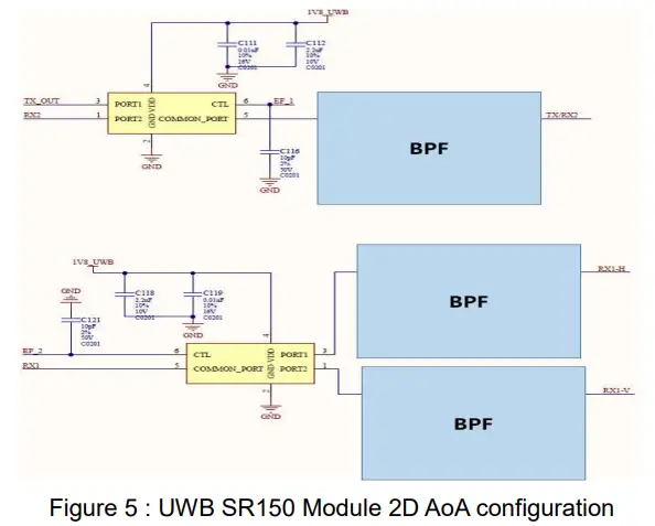
RF connections
SR150 has 2 RF inputs (RX1, RX2) and one RF output (TX). Our module has changed RF Pass to Tx/Rx2, Rx1_V and Rx1_H by embedded RF Switch. These 3 RF ports can be connected to 3 antennas. RX1_V and RX1_H path was guarantee the same path characteristics (insertion loss, electrical delay). Connecting each Antenna to the Tx/Rx2 pad and Rx1_H pad are fulfilled ranging and 2D AoA.
Routing of RF paths and layout recommendations:
- RF paths must be perfectly symmetrical in terms of components used, placement and copper pads and shapes (transmission lines) joining them.
- RF traces must be 50Ω and components should be matched to 50Ω to minimize mismatch losses. The transmission line and reference plane layers must be at stitched thoroughly with ground vias.
- Maintain good isolation between TX, RX2 and RX1.
- The antenna structure should follow the manufacturer’s guidelines with regards to position with respect to the ground plane and the printed circuit board, thickness of the PCB and dielectric constant. Where these are driven by other factors adjustments to the antenna structure may be necessary.
- No component or ground plane should be placed in the antenna area.
- It is highly desirable to shield the UWB radio to prevent unwanted emissions and to provide immunity from external sources of interference.
RF Antenna
In order to guarantee the RF performance of ranging and Angle of Arrival (AoA), the design and layout of the antenna must respect following recommendations. Antenna designs must be studied (simulated) by the customer to meet these requirements in their setup.
- Gain:
Same gain in all directions of concern (for AoA). Ideally gain should close to 0dBi or higher in the direction of use (in all directions of concern for ToF). Good gain and efficiency ensures optimal receiver performance and low TX power consumption. Ensure that the radiation gain in the direction of non-concern is as low as possible to not receive unwanted signals. - Isotropy:
Hemispheric isotropic Antenna Radiation Pattern in the direction in which the device wants to locate the other device (3D). Nulls <-10dBr in the pattern are undesirable as they represent phase changes that will introduce an error in the AoA calculations. Isotropic Group-Delay in all directions of concern (for ToF). - Antenna Separation:
The antenna separation should be less than half a wavelength at the highest frequency of operation.
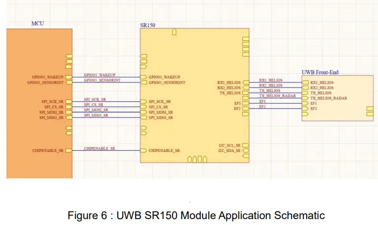
Application Schematic
Copyright © 2010 AMOSENSE Co., Ltd.
AMOSENSE Confidential. All characteristics and specifications are subject to change without notice: http://www.amosense.co.kr


