u-blox LARA-R2/R6 Migration
Abstract
This document provides hardware guidelines to migrate from u-blox LARA-R2 series region-specific LTE Cat 1 / 3G / 2G modules to LARA-R6 series global and multi-region LTE Cat 1 / 3G / 2G modules, all which are designed in the compact LARA form factor.
Document information
| Title | LARA-R2/R6 migration guide | |
| Subtitle | HW guidelines to migrate from LARA-R2 to LARA-R6 | |
| Document type | Application note | |
| Document number | UBX-21010015 | |
| Revision and date | R02 | 05-May-2022 |
| Disclosure restriction | C1-Public | |
| Product status | Corresponding content status | |
| Functional sample | Draft | For functional testing. Revised and supplementary data will be published later. |
| In development / Prototype | Objective specification | Target values. Revised and supplementary data will be published later. |
| Engineering sample | Advance information | Data based on early testing. Revised and supplementary data will be published later. |
| Initial production | Early production information | Data from product verification. Revised and supplementary data may be published later. |
| Mass production / End of life | Production information | Document contains the final product specification. |
This document applies to the following products:
| Product name | Ordering code | Product Status |
| LARA-R202 | LARA-R202-02B | End of life |
| LARA-R202-82B | End of life | |
| LARA-R202-03B | End of life | |
| LARA-R203 | LARA-R203-02B | End of life |
| LARA-R203-03B | End of life | |
| LARA-R204 | LARA-R204-02B | End of life |
| LARA-R211 | LARA-R211-02B | End of life |
| LARA-R211-03B | End of life | |
| LARA-R220 | LARA-R220-62B | End of life |
| LARA-R280 | LARA-R280-02B | End of life |
| LARA-R281 | LARA-R281-02B | End of life |
| LARA-R6001 | LARA-R6001-00B | Prototype |
| LARA-R6001D | LARA-R6001D-00B | Initial production |
| LARA-R6401 | LARA-R6401-00B | Prototype |
| LARA-R6401D | LARA-R6401D-00B | Engineering sample |
| LARA-R6801 | LARA-R6801-00B | Functional sample |
u-blox or third parties may hold intellectual property rights in the products, names, logos and designs included in this document. Copying, reproduction, modification or disclosure to third parties of this document or any part thereof is only permitted with the express written permission of u-blox.
The information contained herein is provided “as is” and u-blox assumes no liability for its use. No warranty, either express or implied, is given, including but not limited to, with respect to the accuracy, correctness, reliability and fitness for a particular purpose of the information. This document may be revised by u-blox at any time without notice. For the most recent documents, visit www.u-blox.com.
Copyright © u-blox AG.
LARA-R2 / LARA-R6 modules description
- The u-blox LARA-R2 series comprises single-mode and multi-mode modules supporting LTE Cat 1 in FDD multi-band, 3G UMTS/HSPA in FDD multi-band, 2G GSM/GPRS/EGPRS in dual-band, providing the ideal solution for region-specific coverage.
- The u-blox LARA-R6 series comprises single-mode and multi-mode modules supporting LTE Cat 1 in FDD / TDD multi-band, 3G UMTS/HSPA in FDD multi-band, 2G GSM/GPRS/EGPRS in quad-band, providing the ideal solution for global and multi-regional coverage.
- All the LARA-R2 and LARA-R6 series modules are available in the same small LARA LGA form-factor (26.0 x 24.0 mm, 100-pin), easy to integrate in compact designs.
- LARA series modules are form-factor compatible with the u-blox SARA, LISA and TOBY cellular module families, facilitating a seamless drop-in migration from other u-blox LPWA, GSM/GPRS, CDMA, UMTS/HSPA and LTE modules.
- Table 1 summarizes the main features and interfaces of LARA-R2 and LARA-R6 series modules. Some features are not supported by older product versions of the corresponding LARA-R2 series product variant. For more details, see LARA-R2 series data sheet [1].
| Model | Region | Radio Access Technology | Positioning | Interfaces | Features | Grade | ||||||||||||||||||||||||||||
|
LTE FDD bands | LTE TDD bands | UMTS/HSPA FDD bands | GSM/GPRS/EGPRS bands | Integrated GNSS receiver | External GNSS control | AssistNow Software | CellLocate® | CART | USB 2.0 | I2C | GPIOs | Digital audio | VoLTE | CSFB | Rx Diversity | Dual stack IPv4 / IPv6 | TCPIP, UDP/IP, HTTP/FTP | TSL/DTLS | MQTT | LwM2M | FOAT / FOTA / uFOTA | Device and Data Security | 3GPP Power Saving Mode | eDRX | Last gasp | Network indication | Antenna and SIM detection | Antenna dynamic tuning | Jamming detection | Standard | Professional | Automotive | ||
| LARA-R202 | North America | 2,4,5,12 | 2,5 | ● | ● | ● | 2 | 1 | 1 | 9 | ● | ● | ● | ● | ● | ● | ● | ● | ● | ● | ● | |||||||||||||
| LARA-R203 | North America | 2,4,12 | ● | ● | ● | 2 | 1 | 1 | 9 | ● | ● | ● | ● | ● | ● | ● | ● | ● | ● | |||||||||||||||
| LARA-R204 | North America | 4,13 | 1 | 1 | 1 | 9 | ● | ● | ● | ● | ● | ● | ● | ● | ||||||||||||||||||||
| LARA-R211 | EMEA | 3,7,20 | Dual | ● | ● | ● | 2 | 1 | 1 | 9 | ● | ● | ● | ● | ● | ● | ● | ● | ● | ● | ● | |||||||||||||
| LARA-R220 | Japan | 1,19 | ● | ● | ● | 1 | 1 | 1 | 9 | ● | ● | ● | ● | ● | ● | ● | ● | |||||||||||||||||
| LARA-R280 | APAC | 3,8,28 | 1 | ● | ● | ● | 1 | 1 | 1 | 9 | ● | ● | ● | ● | ● | ● | ● | ● | ● | ● | ||||||||||||||
| LARA-R281 | EMEA | 1,3,8 20,28 | 1 | ● | ● | ● | 1 | 1 | 1 | 9 | ● | ● | ● | ● | ● | ● | ● | ● | ● | ● | ||||||||||||||
| LARA-R6001 | Global | 1,2,3,4,5,7,8 12,13,18,19 20,26,28 | 38,39 40,41 | 1,2 5,8 | Quad | ● | ● | ● | 2 | 1 | 1 | 9 | ● | ● | ● | ● | ● | ● | ● | ● | ● | ● | ● | ○ | ● | ● | ● | ● | ● | ● | ||||
| LARA-R6001D | Global | 1,2,3,4,5,7,8 12,13,18,19 20,26,28 | 38,39 40,41 | 1,2 5,8 | Quad | ● | ● | ● | 2 | 1 | 1 | 9 | ● | ● | ● | ● | ● | ● | ● | ● | ○ | ● | ● | ● | ● | ● | ● | |||||||
| LARA-R6401 | North America | 2,4,5,12,13,14 66,71 | ● | ● | ● | 2 | 1 | 1 | 9 | ● | ● | ● | ● | ● | ● | ● | ● | ● | ● | ○ | ● | ● | ● | ● | ● | ● | ● | |||||||
| LARA-R6401D | North America | 2,4,5,12,13,14 66,71 | ● | ● | ● | 2 | 1 | 1 | 9 | ● | ● | ● | ● | ● | ● | ● | ● | ○ | ● | ● | ● | ● | ● | ● | ● | |||||||||
| LARA-R6801 | Multi Region | 1,2,3,4,5,7,8 18,19,20,26,28 | 1,2 5,8 | Quad | ● | ● | ● | 2 | 1 | 1 | 9 | ● | ● | ● | ● | ● | ● | ● | ● | ● | ● | ● | ○ | ● | ● | ● | ● | ● | ● | |||||
Table 1: LARA-R2 and LARA-R6 series main features summary (● = supported, ○ = planned)
- LARA-R2 series region-specific LTE Cat 1 / 3G / 2G modules:
- LARA-R202, designed mainly for operation in America, supporting four LTE Cat 1 FDD bands plus two 3G bands
- LARA-R203, designed for operation in North America, supporting three LTE Cat 1 FDD bands
- LARA-R204, designed for operation in USA, supporting two Verizon LTE Cat 1 FDD bands
- LARA-R211, designed mainly for operation in EMEA, supporting three LTE Cat 1 FDD bands plus two 2G bands
- LARA-R220, designed for operation in Japan, supporting two DoCoMo LTE Cat 1 FDD bands
- LARA-R280, designed mainly for operation in APAC, supporting three LTE Cat 1 FDD bands plus one 3G band
- LARA-R281, designed mainly for operation in EMEA, supporting five LTE Cat 1 FDD bands plus one 3G band
LARA-R6 series global and multi-region LTE Cat 1 / 3G / 2G modules:
- LARA-R6001, designed for world-wide operation, supporting eighteen LTE Cat 1 FDD / TDD bands plus four 3G bands and four 2G bands for global coverage
- LARA-R6001D, data-only variant of LARA-R6001. Designed for world-wide operation, supporting eighteen LTE Cat 1 FDD / TDD bands plus four 3G bands and four 2G bands for global coverage
- LARA-R6401, designed mainly for operation in America, supporting eight LTE Cat 1 FDD bands
- LARA-R6401D, data-only varaint of LARA-R6401. Designed mainly for operation in America, supporting eight LTE Cat 1 FDD bands
- LARA-R6801, designed for multi-regional operation, in EMEA, APAC, Japan and Latin America, supporting twelve LTE Cat 1 FDD bands plus four 3G bands and four 2G bands
- Table 2 summarizes the LTE, 3G and 2G characteristics of LARA-R2 and LARA-R6 modules.
| 4G LTE | 3G UMTS/HSDPA/HSUPA 1 | 2G GSM/GPRS/EDGE 2 |
| Long Term Evolution (LTE) Evolved UTRA (E-UTRA) Frequency Division Duplex (FDD) Time Division Duplex (TDD)3 DL Rx diversity | High Speed Packet Access (HSPA) UMTS Terrestrial Radio Access (UTRA) Frequency Division Duplex (FDD) DL Rx diversity | Enhanced Data rate GSM Evolution (EDGE) GSM EGPRS Radio Access (GERA) Time Division Multiple Access (TDMA) DL Advanced Rx Performance Phase 1 |
| LTE Power Class · Power Class 3 (23 dBm) | UMTS/HSDPA/HSUPA Power Class · Class 3 (24 dBm) | GSM/GPRS (GMSK) Power Class · Class 4 (33 dBm) for 850/900 band · Class 1 (30 dBm) for 1800/1900 band EDGE (8-PSK) Power Class · Class E2 (27 dBm) for 850/900 band · Class E2 (26 dBm) for 1800/1900 band |
| Data rate · LTE category 1: up to 10.3 Mbit/s DL, up to 5.2 Mbit/s UL | Data rate · HSDPA category 8: up to 7.2 Mbit/s DL · HSUPA category 6: up to 5.76 Mbit/s UL | Data rate · GPRS multi-slot class 33, CS1-CS4, up to 107 kbit/s DL, 85.6 kbit/s UL · EDGE multi-slot class 33, MCS1-MCS9, up to 296 kbit/s DL, 236.8 kbit/s UL |
Table 2: LARA-R2 and LARA-R6 modules LTE, 3G and 2G characteristics summary
- 3G RAT is not supported by LARA-R203, LARA-R204, LARA-R211, LARA-R220, LARA-R6401 or LARA-R6401D modules.
- 2G RAT is not supported by LARA-R202, LARA-R203, LARA-R204, LARA-R220, LARA-R280, LARA-R281, LARA-R6401 or LARA-R6401D modules.
- LTE TDD radio access technology is not supported by LARA-R2 series, LARA-R6401, or LARA-R6801 modules.
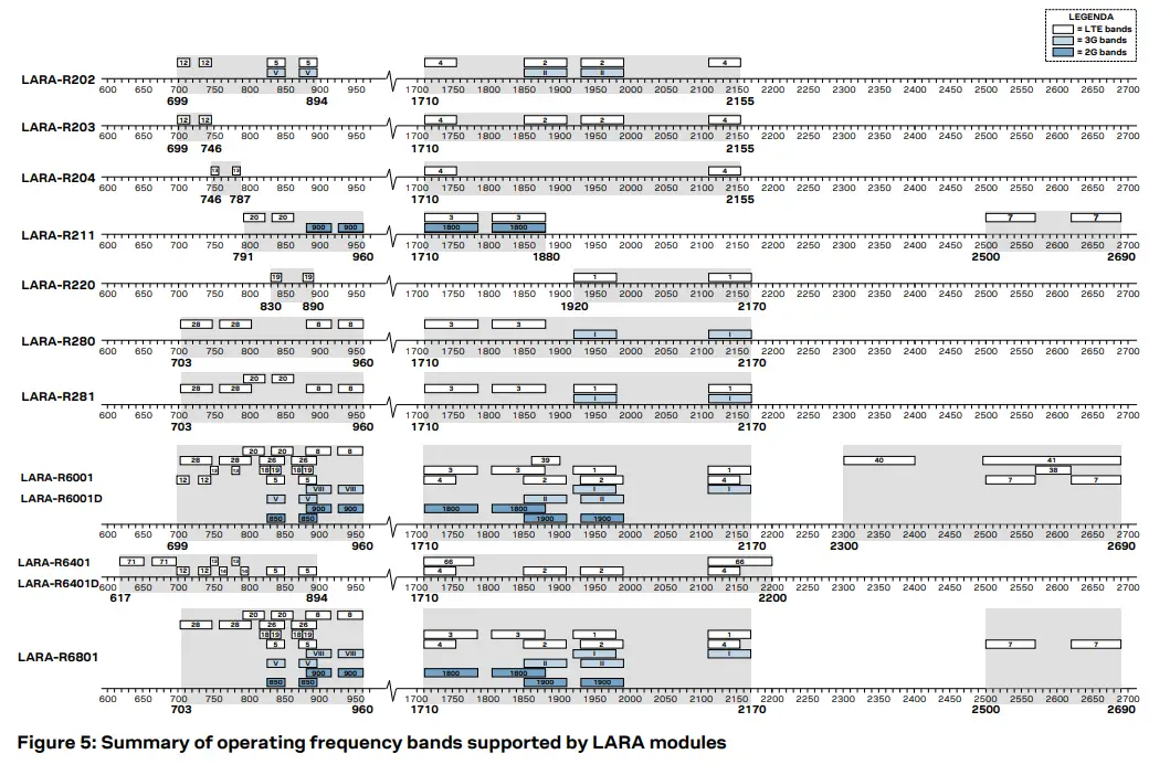
Table 3 summarizes LARA-R2, and LARA-R6 series modules cellular RF bands.
| Module | Region | LTE FDD bands | LTE TDD bands | 3G bands | 2G bands |
| LARA-R202 | North America | 12 (700 MHz) 5 (850 MHz) 4 (1700 MHz) 2 (1900 MHz) | 5 (850 MHz) 2 (1900 MHz) | ||
| LARA-R203 | North America | 12 (700 MHz) 4 (1700 MHz) 2 (1900 MHz) | |||
| LARA-R204 | North America | 13 (700 MHz) 4 (1700 MHz) | |||
| LARA-R211 | Europe, Middle East, Africa | 20 (800 MHz) 3 (1800 MHz) 7 (2600 MHz) | GSM 850 DCS 1800 | ||
| LARA-R220 | Japan | 19 (800 MHz) 1 (2100 MHz) | |||
| LARA-R280 | Asia-Pacific | 28 (700 MHz) 8 (900 MHz) 3 (1800 MHz) | 1 (2100 MHz) | ||
| LARA-R281 | Europe, Middle East, Africa | 28 (700 MHz) 20 (800 MHz) 8 (900 MHz) 3 (1800 MHz) 1 (2100 MHz) | 1 (2100 MHz) | ||
| LARA-R6001 LARA-R6001D | Global | 12 (700 MHz) 28 (700 MHz) 13 (700 MHz) 20 (800 MHz) 18 (800 MHz) 19 (800 MHz) 26 (850 MHz) 5 (850 MHz) 8 (900 MHz) 4 (1700 MHz) 3 (1800 MHz) 2 (1900 MHz) 1 (2100 MHz) 7 (2600 MHz) | 39 (1900 MHz) 40 (2300 MHz) 41 (2600 MHz) 38 (2600 MHz) | 5 (850 MHz) 8 (900 MHz) 2 (1900 MHz) 1 (2100 MHz) | GSM 850 E-GSM 900 DCS 1800 PCS 1900 |
| LARA-R6401 LARA-R6401D | North America | 71 (600 MHz) 12 (700 MHz) 13 (700 MHz) 14 (700 MHz) 5 (850 MHz) 4 (1700 MHz) 66 (1700 MHz) 2 (1900 MHz) | |||
| LARA-R6801 | Europe, Middle East, Africa Asia-Pacific Japan Latin America | 28 (750 MHz) 20 (800 MHz) 18 (800 MHz) 19 (800 MHz) 26 (850 MHz) 5 (850 MHz) 8 (900 MHz) 4 (1700 MHz) 3 (1800 MHz) 2 (1900 MHz) 1 (2100 MHz) 7 (2600 MHz) | 5 (850 MHz) 8 (900 MHz) 2 (1900 MHz) 1 (2100 MHz) | GSM 850 E-GSM 900 DCS 1800 PCS 1900 |
Table 3: LARA-R2 and LARA-R6 series modules cellular RF bands summary
Migration between LARA modules
Overview
The u-blox LARA form factor (26.0 x 24.0 mm, 100-pin LGA) includes the following series of modules, with compatible pin assignments as described in Figure 1, so that the modules can be alternatively mounted on a single application PCB using exactly the same copper, solder resist and paste mask.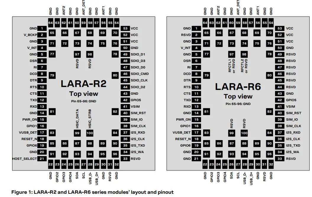
Table 4 summarizes the interfaces supported by LARA series modules:
| LARA-R2 series | LARA-R6 series | |
| VCC module supply input | ● | ● |
| V_INT 1.8V supply output | ● | ● |
| V_BCKP RTC supply input/output | ● | |
| ANT1 main RF input/output | ● | ● |
| ANT2 RF Rx diversity input | ● | ● |
| ANT_DET antenna detection input | ● | ● |
| Antenna dynamic tuning (RFCTL1 / RFCTL2) | ● 4 | |
| PWR_ON input | ● | ● |
| RESET_N input | ● | ● |
| SIM interface | ● | ● |
| SIM detection | ● | ● |
| Main primary 8-wire UART | ● | ● |
| Auxiliary secondary 4-wire UART | ● | |
| Auxiliary secondary 2-wire UART | ● |
- LARA-R6401 and LARA-R6401D only
| LARA-R2 series | LARA-R6 series | |
| USB High-Speed Interface | ● | ● |
| I2C interface | ● | ● |
| Digital Audio Interface | ● | ● 5 |
| Clock output | ● | ● 5 |
| GPIOs | ● | ● |
Table 4: Summary of interfaces supported by LARA-R2/R6 migration guide modules
The LARA modules are also form-factor compatible with the u-blox SARA, LISA, and TOBY cellular module families: although each has a different form factor, the footprints for the TOBY, LISA, LARA, and SARA modules have been developed to ensure layout compatibility.
With the u-blox “nested design” solution, any TOBY, LISA, SARA, or LARA module can be alternatively mounted on the same space of a single “nested” application board as described in Figure 2, enabling straightforward development of products supporting different cellular radio access technologies.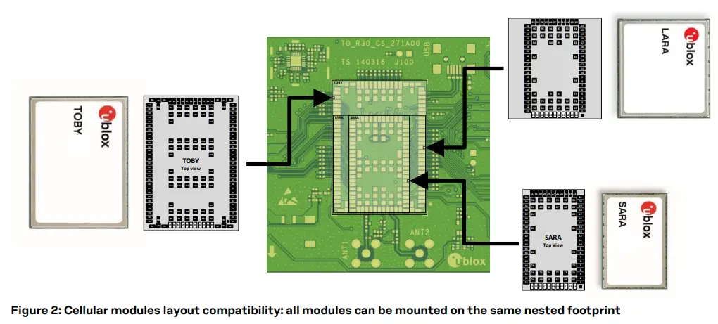
In detail, as described in Figure 3, a different top-side stencil (paste mask) is needed for each u-blox module form factor (TOBY, LISA, SARA, and LARA) to be alternatively mounted on the same space of a single “nested” application board.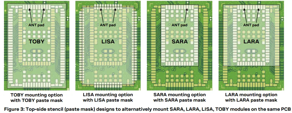
Detailed guidelines to implement a nested application board, a comprehensive description of the u-blox reference nested design and detailed comparisons between the u-blox SARA, LARA, LISA, and TOBY modules are provided in the Nested design application note [3].
Pin-out comparison between LARA modules
Table 5 shows a pin-out comparison between LARA-R2 and LARA-R6 series modules.
| No | LARA-R2 series | LARA-R6 series |
| 1 | GND | GND |
| Ground | Ground | |
| 2 | V_BCKP | RSVD |
| RTC supply I/O | Reserved for future use. Internally not connected. | |
| 3 | GND | GND |
| Ground | Ground | |
| 4 | V_INT | V_INT |
| 1.8 V (typical) supply output Generated by internal DC/DC step-down regulator, when the module is turned on. Test point recommended | 1.8 V (typical) supply output Generated by internal LDO linear regulator, when the module is turned on. Test point recommended | |
| 5 | GND | GND |
| Ground | Ground | |
| 6 | DSR | DSR |
| Main primary UART Data Set Ready output (push-pull, idle high, active low)
V_INT voltage supply domain (1.8 V) Output driver strength: 6 mA Internal active pull-up strength: ~7.5 kΩ | Main primary UART Data Set Ready output (push-pull, idle high, active low) Alternative function: Second auxiliary UART HW flow control input (idle high, active low, with internal active pull-up enabled). V_INT voltage supply domain (1.8 V) Output driver strength: 2 mA Internal active pull-up strength: ~100 kΩ | |
| 7 | RI | RI |
| Main primary UART Ring Indicator output (push-pull, idle high, active low)
V_INT voltage supply domain (1.8 V) Output driver strength: 6 mA | Main primary UART Ring Indicator output (push-pull, idle high, active low) Alternative function: Second auxiliary UART HW flow control output (push-pull, idle high, active low). V_INT level (1.8 V) Output driver strength: 2 mA | |
| 8 | DCD | DCD |
| Main primary UART Data Carrier Detect output (push-pull, idle high, active low)
V_INT voltage supply domain (1.8 V) Output driver strength: 6 mA | Main primary UART Data Carrier Detect output (push-pull, idle high, active low) Alternative function: Second auxiliary UART data output (push-pull, idle high, active low). V_INT voltage supply domain (1.8 V) Output driver strength: 2 mA | |
| 9 | DTR | DTR |
| Main primary UART Data Terminal Ready input (idle high, active low, with internal active pull-up enabled) to be set low to activate the greeting text.
V_INT voltage supply domain (1.8 V) Internal active pull-up strength: ~7.5 kΩ | Main primary UART Data Terminal Ready input (idle high, active low, with internal active pull-up enabled) to be set low to activate the greeting text. Alternative function: Second auxiliary UART data input (idle high, active low, with internal active pull-up enabled). V_INT voltage supply domain (1.8 V) Internal active pull-up strength: ~100 kΩ |
| No | LARA-R2 series | LARA-R6 series |
| 10 | RTS | RTS |
| Main primary UART HW flow control input (idle high, active low, with internal active pull-up enabled) V_INT voltage supply domain (1.8 V) Internal active pull-up strength: ~7.5 kΩ | Main primary UART HW flow control input (idle high, active low, with internal active pull-up enabled) V_INT voltage supply domain (1.8 V) Internal active pull-up strength: ~100 kΩ | |
| 11 | CTS | CTS |
| Main primary UART HW flow control output (push-pull, idle high, active low). V_INT voltage supply domain (1.8 V) Output driver strength: 6 mA | Main primary UART HW flow control output (push-pull, idle high, active low). V_INT voltage supply domain (1.8 V) Output driver strength: 2 mA | |
| 12 | TXD | TXD |
| Main primary UART data input (idle high, active low, with internal active pull-up enabled). V_INT voltage supply domain (1.8 V) Internal active pull-up strength: ~7.5 kΩ | Main primary UART data input (idle high, active low, with internal active pull-up enabled). V_INT voltage supply domain (1.8 V) Internal active pull-up strength: ~100 kΩ | |
| 13 | RXD | RXD |
| Main primary UART data output (push-pull, idle high, active low). V_INT voltage supply domain (1.8 V) Output driver strength: 6 mA | Main primary UART data output (push-pull, idle high, active low). V_INT voltage supply domain (1.8 V) Output driver strength: 2 mA | |
| 14 | GND | GND |
| Ground | Ground | |
| 15 | PWR_ON | PWR_ON |
| Power-on/off input (idle high, active low, with 10 kΩ internal pull-up). V_BCKP voltage supply domain (1.8 V) L-level: -0.30 ÷ 0.54 V L-level pulse time to trigger switch on: 50 µs min L-level pulse time to trigger graceful switch off: 1.0 s min No external pull-up to be connected Test point recommended | Power-on/off input (idle high, active low, with ~200 kΩ internal pull-up). Internal voltage supply domain (~0.8 V at the pin in idle) L-level: -0.30 ÷ 0.35 V L-level pulse time to trigger switch on: 0.15 s min ÷ 3.2 s max L-level pulse time to trigger graceful switch off: 1.5 s min No external pull-up to be connected Test point recommended | |
| 16 | GPIO1 | GPIO1 |
| GPIO configurable as Input, Output, Network status indication, external GNSS supply enable. Default: tri-stated with internal pull-down enabled. V_INT voltage supply domain (1.8 V) Push-pull output type. Output driver strength: 6 mAInternal active pull-up strength: ~17 kΩ | GPIO configurable as Input, Output, Network status indication, external GNSS supply enable. Default: tri-stated with internal pull-down enabled. V_INT voltage supply domain (1.8 V) Push-pull output type. Output driver strength: 2 mA Internal active pull-up/down strength: ~100 kΩ | |
| 17 | VUSB_DET | VUSB_DET |
| 5 V sense input to detect USB host and enable the USB. H-level: 1.5 ÷ 5.25 V Test point highly recommended | 5 V sense input to detect USB host and enable the USB H-level: 1.5 ÷ 5.25 V Test point highly recommended | |
| 18 | RESET_N | RESET_N |
| Abrupt emergency reset shutdown input (idle high, active low, with 10 kΩ internal pull-up). V_BCKP voltage supply domain (1.8 V) L-level: -0.30 ÷ 0.54 V L-level time to trigger abrupt PMU and module reboot: 50 ms min Test point recommended | Abrupt emergency reset shutdown input (idle high, active low, with ~37 kΩ internal active pull-up). Internal voltage supply domain (~1.8 V at the pin in idle) L-level: -0.30 ÷ 0.63 V L-level time to trigger graceful module reboot: 50 ms min ÷ 6 s max L-level time to trigger abrupt module switch off: 10 s min Test point recommended |
| No | LARA-R2 series | LARA-R6 series |
| 19 | GPIO6 | GPIO6 |
| 13 or 26 MHz clock output enabled by AT command. Default: tri-stated with internal pull-down enabled. V_INT voltage supply domain (1.8 V) Push-pull output type. Driver strength: 4 mA Internal active pull-up/down strength: ~7.5 kΩ | 12.288 MHz clock output enabled by AT command 6. Default: tri-stated with internal pull-down enabled. V_INT voltage supply domain (1.8 V) Push-pull output type. Output driver strength: 2 mA Internal active pull-up/down strength: ~100 kΩ | |
| 20 | GND | GND |
| Ground | Ground | |
| 21 | HOST_SELECT | GND |
| Selection of module / host processor configuration function not supported by current FW version. Default: tri-stated with internal pull-down enabled. V_INT voltage supply domain (1.8 V) Internal active pull-up/down strength: ~7.5 kΩ | Ground | |
| 22 | GND | GND |
| Ground | Ground | |
| 23 | GPIO2 | GPIO2 |
| GPIO configurable as Input, Output, Network status indication output, external GNSS supply enable output. Default: output for external GNSS supply enable control V_INT voltage supply domain (1.8 V) Push-pull output type. Output driver strength: 6 mA Internal active pull-up/down strength: ~7.5 kΩ | GPIO configurable as Input, Output, Network status indication output, external GNSS supply enable output. Default: output for external GNSS supply enable control V_INT voltage supply domain (1.8 V) Push-pull output type. Output driver strength: 2 mA Internal active pull-up/down strength: ~100 kΩ | |
| 24 | GPIO3 | GPIO3 |
| GPIO configurable as Input, Output, Network status indication output, external GNSS supply enable output, external GNSS data ready input.
Default: input for external GNSS Tx data ready V_INT voltage supply domain (1.8 V) Push-pull output type. Output driver strength: 6 mA Internal active pull-up/down strength: ~7.5 kΩ | GPIO configurable as Input, Output, Network status indication output, external GNSS supply enable output, external GNSS data ready input, Last gasp trigger input, Faster and safe power-off trigger input. Default: input for external GNSS Tx data ready V_INT voltage supply domain (1.8 V) Push-pull output type. Output driver strength: 2 mA Internal active pull-up/down strength: ~100 kΩ | |
| 25 | GPIO4 | GPIO4 |
| GPIO configurable as Input, Output, Network status indication output, external GNSS supply enable output. Default: output / low V_INT voltage supply domain (1.8 V) Push-pull output type. Output driver strength: 6 mA Internal active pull-up/down strength: ~7.5 kΩ | GPIO configurable as Input, Output, Network status indication output, external GNSS supply enable output. Default: output / low V_INT voltage supply domain (1.8 V) Push-pull output type. Output driver strength: 2 mA Internal active pull-up/down strength: ~100 kΩ | |
| 26 | SDA | SDA |
| I2C data (open drain, idle high, active low, no internal pull-up). Alternative function: Second auxiliary UART data input (idle high, active low, with internal active pull-up enabled). V_INT voltage supply domain (1.8 V) | I2C data (open drain, idle high, active low, 2.2 kΩ internal pull-up).
V_INT voltage supply domain (1.8 V) |
| No | LARA-R2 series | LARA-R6 series |
| 27 | SCL | SCL |
| I2C clock (open drain, idle high, active low, no internal pull-up). Alternative function: Second auxiliary UART data output (push-pull, idle high, active low). V_INT voltage supply domain (1.8 V) | I2C clock (open drain, idle high, active low, 2.2 kΩ internal pull-up).
V_INT voltage supply domain (1.8 V) | |
| 28 | USB_D- | USB_D- |
| USB data I/O (D-) High-speed USB 2.0 Test point highly recommended | USB data I/O (D-) High-speed USB 2.0 Test point highly recommended | |
| 29 | USB_D+ | USB_D+ |
| USB data I/O (D+) High-speed USB 2.0 Test point highly recommended | USB data I/O (D+) High-speed USB 2.0 Test point highly recommended | |
| 30 | GND | GND |
| Ground | Ground | |
| 31 | RSVD | RSVD |
| Reserved for future use Internally not connected | Reserved for future use Internally not connected | |
| 32 | GND | GND |
| Ground | Ground | |
| 33 | RSVD | RSVD |
| Reserved use It must be connected to ground | Reserved use Test point highly recommended | |
| 34 | I2S_WA | I2S_WA 7 |
| I2S Word Alignment, alternatively configurable GPIO. Default: I2S Word Alignment V_INT voltage supply domain (1.8 V) Push-pull output type. Output driver strength: 6 mA Internal active pull-up/down strength: ~7.5 kΩ | I2S Word Alignment, alternatively configurable GPIO. Default: I2S Word Alignment V_INT voltage supply domain (1.8 V) Push-pull output type. Output driver strength: 2 mA Internal active pull-up/down strength: ~7.5 kΩ | |
| 35 | I2S_TXD | I2S_TXD 7 |
| I2S data output, alternatively configurable GPIO. Default: I2S data output V_INT voltage supply domain (1.8 V) Push-pull output type. Output driver strength: 6 mA Internal active pull-up/down strength: ~7.5 kΩ | I2S data output, alternatively configurable GPIO. Default: I2S data output V_INT voltage supply domain (1.8 V) Push-pull output type. Output driver strength: 2 mA Internal active pull-up/down strength: ~100 kΩ | |
| 36 | I2S_CLK | I2S_CLK 7 |
| I2S clock, alternatively configurable GPIO. Default: I2S clock V_INT voltage supply domain (1.8 V) Push-pull output type. Output driver strength: 6 mA Internal active pull-up/down strength: ~7.5 kΩ | I2S clock, alternatively configurable GPIO. Default: I2S clock V_INT voltage supply domain (1.8 V) Push-pull output type. Output driver strength: 2 mA Internal active pull-up/down strength: ~100 kΩ | |
| 37 | I2S_RXD | I2S_RXD 7 |
| I2S data input, alternatively configurable GPIO. Default: I2S data input V_INT voltage supply domain (1.8 V) Push-pull output type. Output driver strength: 6 mA Internal active pull-up/down strength: ~7.5 kΩ | I2S input, alternatively configurable GPIO. Default: I2S data input V_INT voltage supply domain (1.8 V) Push-pull output type. Output driver strength: 2 mA Internal active pull-up/down strength: ~100 kΩ |
| No | LARA-R2 series | LARA-R6 series |
| 38 | SIM_CLK | SIM_CLK |
| Clock output for external 1.8 V / 3 V SIM card/chip | Clock output for external 1.8 V / 3 V SIM card/chip | |
| 39 | SIM_IO | SIM_IO |
| I/O data line for external 1.8 V / 3 V SIM card/chip Internal pull-up: 4.7 kΩ | I/O data line for external 1.8 V / 3 V SIM card/chip Internal pull-up: 4.7 kΩ | |
| 40 | SIM_RST | SIM_RST |
| Reset output for external 1.8 V / 3 V SIM card/chip | Reset output for external 1.8 V / 3 V SIM card/chip | |
| 41 | VSIM | VSIM |
| Supply output for external 1.8 V / 3 V SIM card/chip | Supply output for external 1.8 V / 3 V SIM card/chip | |
| 42 | GPIO5 | GPIO5 |
| GPIO configurable as Input, Output, SIM detection input. Default: SIM detection input V_INT voltage supply domain (1.8 V) Push-pull output type. Output driver strength: 6 mA Internal active pull-up/down strength: ~7.5 kΩ | GPIO configurable as Input, Output, SIM detection input. Default: SIM detection input V_INT voltage supply domain (1.8 V) Push-pull output type. Output driver strength: 2 mA Internal active pull-up/down strength: ~100 kΩ | |
| 43 | GND | GND |
| Ground | Ground | |
| 44 | SDIO_D2 | RSVD |
| SDIO serial data [2], not supported by current FW Default: tri-stated with internal pull-down enabled. | Reserved for future use | |
| 45 | SDIO_CLK | RSVD |
| SDIO serial clock, not supported by current FW Default: tri-stated with internal pull-down enabled. | Reserved for future use | |
| 46 | SDIO_CMD | RSVD |
| SDIO command, not supported by current FW Default: tri-stated with internal pull-down enabled. | Reserved for future use | |
| 47 | SDIO_D0 | RSVD |
| SDIO serial data [0], not supported by current FW Default: tri-stated with internal pull-down enabled. | Reserved for future use | |
| 48 | SDIO_D3 | RSVD |
| SDIO serial data [3], not supported by current FW Default: tri-stated with internal pull-down enabled. | Reserved for future use | |
| 49 | SDIO_D1 | RSVD |
| SDIO serial data [1], not supported by current FW Default: tri-stated with internal pull-down enabled. | Reserved for future use | |
| 50 | GND | GND |
| Ground | Ground | |
| 51 | VCC | VCC |
| Supply input for the whole module Normal operating range: 3.3 ÷ 4.4 V Extended operating range: 3.0 ÷ 4.5 V LARA-R211: Supply input for baseband PMU part | Supply input for baseband PMU part Normal operating range: 3.3 ÷ 4.5 V Extended operating range: 3.1 ÷ 4.5 V | |
| 52 | VCC | VCC |
| Supply input for the whole module Normal operating range: 3.3 ÷ 4.4 V Extended operating range: 3.0 ÷ 4.5 V LARA-R211: Supply for RF Power Amplifiers part | Supply for RF Power Amplifiers part. Normal operating range: 3.3 ÷ 4.5 V Extended operating range: 2.8 ÷ 4.5 V |
| No | LARA-R2 series | LARA-R6 series |
| 53 | VCC | VCC |
| Supply input for the whole module Normal operating range: 3.3 ÷ 4.4 V Extended operating range: 3.0 ÷ 4.5 V LARA-R211: Supply for RF Power Amplifiers part | Supply for RF Power Amplifiers part Normal operating range: 3.3 ÷ 4.5 V Extended operating range: 2.8 ÷ 4.5 V | |
| 54 | GND | GND |
| Ground | Ground | |
| 55 | GND | GND |
| Ground | Ground | |
| 56 | ANT1 | ANT1 |
| RF pin for main Tx / Rx cellular antenna 50 Ω nominal characteristic impedance. | RF pin for main Tx / Rx cellular antenna 50 Ω nominal characteristic impedance. | |
| 57 | GND | GND |
| Ground | Ground | |
| 58 | GND | GND |
| Ground | Ground | |
| 59 | ANT_DET | ANT_DET |
| Input pin for antenna detection (optional function) | Input pin for antenna detection (optional function) | |
| 60 | GND | GND |
| Ground | Ground | |
| 61 | GND | GND |
| Ground | Ground | |
| 62 | ANT2 | ANT2 |
| RF pin for secondary Rx diversity cellular antenna 50 Ω nominal characteristic impedance. | RF pin for secondary Rx diversity cellular antenna 50 Ω nominal characteristic impedance. | |
| 63 | GND | GND |
| Ground | Ground | |
| … | All pins from 63 to 96 are Ground pins | All pins from 63 to 96 are Ground pins |
| 96 | GND | GND |
| Ground | Ground | |
| 97 | RSVD | RSVD 8 |
| Reserved for future use. Internally not connected. | Reserved for future use RFCTL1 9 1.8 V push-pull output to control an antenna tuning IC. | |
| 98 | RSVD | RSVD 8 |
| Reserved for future use. Internally not connected. | Reserved for future use RFCTL2 9 1.8 V push-pull output to control antenna tuning IC. | |
| 99 | HSIC_DATA | RSVD |
| HSIC USB not supported by current FW. | Reserved for future use | |
| 100 | HSIC_STRB | RSVD |
| HSIC USB not supported by current FW. | Reserved for future use |
- Table 5: LARA-R2 and LARA-R6 series modules pin assignment and description, with remarks for migrationu
- For further details regarding characteristics, capabilities, usage or settings applicable for each interface of the LARA-R2 and LARA-R6 series cellular modules, see the related data sheet [1] [4], the related integration manual [2] [5], the related AT commands manual [6] [7], and the nested design application note [3].
Interfaces comparison between LARA modules
VCC module supply input
- As the LARA-R2 and LARA-R6 series modules have compatible power requirements, there are only minor differences in their VCC input voltage ranges and current consumption figures. The same compatible external VCC supply circuit can be implemented for all the LARA modules, as for example the one described in Figure 4.
- The nominal voltage provided at the VCC input pins must be within the related normal operating range limits, and the actual voltage during module operations has to be held above the minimum limit of the extended operating range to avoid the undervoltage switch-off of the module. For the detailed values of VCC input voltage ranges, see
Table 5, or the related module’s data sheet [1] and [4].
- The time-division RF transmission of 2G radio access technology can be up to ~2 W, whereas in 3G or LTE radio access technology it is only up to ~0.25 W. Therefore, the pulse current profile in radio connected mode when a data/voice call is enabled may be significantly higher for cellular modules supporting the 2G radio access technology than for modules that do not have 2G fallback.
- While selecting and designing the supply source for LARA cellular modules, consider with adequate safe margin the maximum current consumption of the LARA cellular module specifically selected, considering the radio access technologies supported by the module.
- For the detailed module’s current consumption figures, see the related module’s data sheet [1] [4]. For additional specific design guidelines, see the related system integration manual [2] [5].
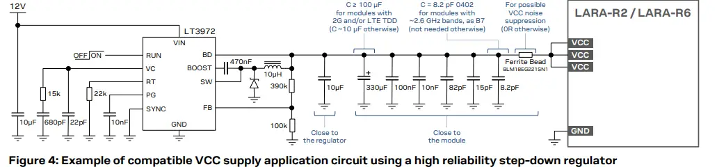
- The VCC supply circuit illustrated in Figure 4 includes capacitors with Self-Resonant Frequency in the supported RF cellular bands, intended to be placed close to the VCC pins of the module, narrowing the VCC line down to the pad of the capacitors, to adequately filter EMI in the supported RF cellular bands. Additionally, a ferrite bead specifically designed to suppress EMI in the GHz band is placed very close to the VCC pins of the module to suppress possible noise from the VCC line.
- Note that the switch-on sequence of LARA-R2 series can be triggered by applying a valid VCC supply, starting a voltage value of less than 2.1 V, and with a fast-rising slope (from 2.3 V to 2.8 V in less than 4 ms) up to the nominal VCC voltage within the normal operating range.
- Instead, LARA-R6 series modules continue to be switched off even after a valid VCC supply has been applied: the PWR_ON input line must be properly toggled low, with valid VCC supply present, to trigger the switch-on sequence of these modules.
V_INT 1.8 V supply output
- LARA-R2 and LARA-R6 series modules provide a 1.8 V supply output at the V_INT pin, which is internally generated when the module is switched on.
- The same voltage domain is used internally to supply the generic digital interfaces of the modules (as the UARTs, I2C, I2S, GPIOs), and therefore it is recommended to use the V_INT supply output to supply the module side of external voltage translators connected to these interfaces of the modules.
- It is recommended to sense the status of the V_INT output to define when the module is switched on, and it is recommended to provide a test point for diagnostic.
V_BCKP RTC supply input/output
- LARA-R2 series modules provide the RTC supply input/output at the V_BCKP pin, which is not available on LARA-R6 series modules, having the same pin internally not connected.
Cellular RF interfaces
- LARA-R2 and LARA-R6 series modules provide the primary RF input/output line at the ANT1 pin, which must be connected to a suitable antenna to transmit and receive cellular RF signals, and they provide the secondary RF input line at the ANT2 pin, which is intended to be connected to an antenna to receive cellular RF signals in LTE and 3G radio access technologies implementing the Rx diversity function.
- The same optional antenna detection circuit can be implemented for LARA-R2 and LARA-R6 series modules using the available optional ANT_DET input pin.
- While selecting the antenna for LARA cellular modules, consider the frequency range supported by each LARA module, as illustrated in Figure 5.
System control interfaces
- The PWR_ON and the RESET_N input lines have internal pull-up resistors on LARA-R2 and LARA-R6 series modules, and both lines are intended to be driven by external open drain drivers: same compatible external circuits can be implemented for all the LARA modules.
- The switch-on sequence of LARA-R2 series modules can be triggered by applying a valid VCC power supply (see section 2.3.1), while LARA-R6 series modules remain switched off after a valid VCC power supply is applied to the modules: the PWR_ON input line must be properly toggled low, with valid VCC supply present, to trigger the switch-on sequence of the modules.
- The PWR_ON input line can be used to trigger the graceful switch-off procedure of the LARA-R2 and LARA-R6 series modules, as an alternative to using the +CPWROFF AT command. Afterwards, the switch-on sequence of modules can be triggered again by properly toggling low PWR_ON input line.
- The assertion or toggling of the RESET_N input line causes different actions:
- the RESET_N line of LARA-R2 series modules triggers an unconditional reboot of the module when toggled, with internal PMU shutdown when set low.
- the RESET_N line of LARA-R6 series modules triggers an unconditional graceful reboot of the module when set low for a short time period.
- the RESET_N line of LARA-R6 series modules triggers an unconditional shutdown of the module when set low for a long time period.
- The timings for proper control of the PWR_ON and RESET_N input lines of LARA-R2 and LARA-R6 series modules are reported in the related data sheet [1] and [4].
- It is recommended to provide test points on the PWR_ON and RESET_N input lines of LARA-R2 and LARA-R6 series modules, to trigger the FW update procedure, and for diagnostic purpose.
SIM interface
- The same compatible external SIM circuit can be implemented for all LARA modules: external 1.8 V and 3.0 V SIM card / IC are supported over the available standardized
- SIM interface (VSIM, SIM_IO, SIM_CLK, SIM_RST pins).
- The same optional SIM detection circuit can be implemented for LARA series modules using the available GPIO5 pin.
UART interfaces
- Main primary UART interface
- LARA-R2 and LARA-R6 modules provide a compatible main 8-wire 1.8 V UART interface including:
- data lines (RXD output, TXD input),
- hardware flow control lines (CTS output, RTS input),
- modem status and control lines (DTR input, DSR output, DCD output, RI output)
- The main primary UART interface supports AT commands and data communication, multiplexer functionality including virtual channel for GNSS tunneling, and FW update by means of FOAT on all the LARA modules.
- Additionally, LARA-R2 series modules support the FW update by means of the u-blox EasyFlash tool, and the diagnostic trace logging functions over the main primary UART interface.
- It is recommended to provide test points on RXD and TXD pins of LARA series modules, for FW update and diagnostic, in particular if the USB interface is connected to the external host processor.
- The primary UART interfaces of LARA series modules are electrically compatible, so that the same compatible external circuit can be used. It is recommended to use the V_INT output to supply the module side of external voltage translators connected to the UART interfaces.
The baud rates and configurations available and supported by LARA-R2 and LARA-R6 series modules for the main primary UART interface may slightly differ:
- LARA-R2 series modules have the automatic baud rate and frame format detection available by default, and they support high-speed UART data rates up to 6.5 Mbit/s.
- LARA-R6 series modules have the 115200 bit/s baud rate and the 8N1 frame format available by default, and they support high-speed UART data rates up to 3.0 Mbit/s.
- For more details about configurations of UART interfaces, see the u-blox AT commands manual [6], +IPR, +ICF, +IFC, &K, \Q, +UPSV, +CMUX, +USIO, +UUSBCONF AT commands, where supported).
Auxiliary UART interface
- LARA-R202, LARA-R203 and LARA-R211 modules provide an auxiliary secondary 2-wire 1.8 V UART serial interface, as alternative function of the I2C interface (SCL and SDA pins) including:
- data lines (SCL pin as AUX UART data output, SDA pin as AUX UART data input)
- LARA-R6 series modules provide an auxiliary secondary 4-wire 1.8 V UART serial interface, as alternative function of the main UART interface DTR, DSR, DCD and RI pins, including:
- data lines (DCD pin as AUX UART data output, DTR pin as AUX UART data input)
- HW flow control lines (RI as AUX UART flow control output, DSR as AUX UART flow control input)
- The data lines of the auxiliary UART interfaces of LARA series modules are electrically compatible, so that the same compatible external circuit can be used. However, the
- AUX UART data input and output functions are available on different pins comparing LARA-R2 and LARA-R6 series modules. It is recommended to use the V_INT output to supply the module side of external voltage translators connected to the AUX UART.
- The baud rates and configurations available and supported by LARA-R2 and LARA-R6 series modules for the auxiliary UART interface may slightly differ: see the u-blox
- AT commands manual [6] (+IPR, +ICF, +IFC, &K, \Q, +USIO, +UUSBCONF AT commands, where supported).
USB interface
- LARA-R2 and LARA-R6 series modules provide a compatible USB 2.0 High-Speed interface including:
- VUSB_DET input pin to detect the presence of an external USB host, and enable the USB interface of the module by applying an external valid USB VBUS voltage (1.5 V minimum, 5.0 V typical),
- USB_D+ and USB_D- data and signaling lines according to the USB 2.0 standard.
- The USB interface supports AT commands and data communication, GNSS tunneling, the FW update by means of FOAT, the FW update by means of the u-blox
- EasyFlash tool, and the diagnostic trace logging functions on all the LARA-R2 and LARA-R6 series modules.
- It is highly recommended to provide accessible test points on VUSB_DET, USB_D+ and USB_D- pins of LARA-R2 and LARA-R6 series modules, for FW update and diagnostic.
- The configurations available and supported by LARA-R2 and LARA-R6 series modules for the USB interface may slightly differ: see the related data sheet of the modules [1] [4], and the u-blox AT commands manual [6] (+USIO, +UUSBCONF AT commands, where supported).
- The USB interface of the LARA-R6 series modules is enabled only if an external voltage detectable as High logic level is applied at the VUSB_DET input during the switch-on boot sequence of the module.
I2C interface
- LARA-R2 and LARA-R6 series modules provide a compatible 1.8 V I2C interface (SDA, SCL pins) available to communicate with external u-blox GNSS chips / modules, and with external compatible
- I2C devices as for example an audio codec: the module acts as an I2C host which can communicate with I2C devices in accordance with the I2C bus specifications.
- LARA-R2 modules do not integrate pull-up resistors on SDA and SCL lines: external pull-up resistors have to be provided accordingly if the I2C interface is used in applications with LARA-R2 modules. Instead, LARA-R6 series modules have internal pull-up resistors on SDA and SCL lines, so there is no necessity of external pull-up resistors.
- It is recommended to use the V_INT output to supply the module side of external voltage translators connected to the I2C interface.
Digital audio interface
- LARA-R2 and LARA-R6 series modules provide a compatible 1.8 V digital audio interface over the I2S_TXD, I2S_RXD, I2S_CLK, I2S_WA pins, that can be configured by AT command to transfer digital audio data to/from an external device as an audio codec.
- The configurations available and supported by LARA-R2 and LARA-R6 series modules for the digital audio interface may slightly differ: see the Audio sections in the u-blox AT commands manual [6].
- LARA-R6001D / LARA-R6401D data-only product versions do not support voice / audio feature.
Clock output
- LARA-R2 and LARA-R6 series modules provide a compatible 1.8 V digital clock output on the GPIO6 pin. This is mainly designed to feed the clock input of an external audio codec, as it can be configured in “Audio dependent” mode (generated only when the audio is active), or in “Continuous” mode.
- LARA-R6001D / LARA-R6401D data-only product versions do not support GPIO6 clock output.
GPIOs
- LARA series modules provide nine compatible 1.8 V GPIO pins (GPIO1-GPIO5, I2S_TXD, I2S_RXD, I2S_CLK, I2S_WA) that can be configured as General Purpose
- Input/Output or to provide custom functions (for further details, see the related data sheet of the modules [1] [4], and the GPIO chapter in the u-blox AT commands manual [6]).
Antenna dynamic tuning
- LARA-R6401 and LARA-R6401D series modules support a wide range of frequencies, from 600 MHz to 2200 MHz. For such modules, to provide more efficient antenna designs over a wide bandwidth, RFCTL1 and RFCTL2 pins can be configured to change their output value in real time according to the operating LTE band in use by the module.
- These pins, paired with an external antenna tuner IC or RF switch, can be used to:
- tune antenna impedance to reduce power losses due to mismatch
- tune antenna aperture to improve total antenna radiation efficiency
- select the optimal antenna for each operating band
Reserved pins
- LARA series modules include pins reserved for future use, marked as RSVD, which can all be left unconnected on the application board, except the RSVD #33 pin:
- It is recommended to connect to ground the RSVD #33 pin of LARA-R2 modules
- It is suggested to connect an accessible test point to the RSVD #33 pin of LARA-R6 modules
Other considerations and test points
- Table 6 lists the interfaces dedicated for special purposes, as the firmware update by means of u-blox EasyFlash tool and/or for diagnostic by means of u-blox m-center tool, on LARA modules.
| Module | FW update by means of u-blox EasyFlash tool | Diagnostic by means of u-blox m-center tool |
| LARA-R2 | USB UART (2-wire data input/output) | USB UART (2-wire data input/output) AUX UART (2-wire data input/output) HSIC |
| LARA-R6 | USB | USB |
- Table 6: Interfaces for FW update and/or diagnostic purposes on LARA modules
- It is highly recommended to provide test points directly connected to the pins with FW update and/or diagnostic functions available (as in particular the VUSB_DET, USB_D+ and USB_D- pins), depending also on which interface of the module is connected to external host application processor (as the RXD and TXD lines of the UART interface also have to be considered).
- Additionally, it is recommended to provide test points directly connected to the following pins of the modules for diagnostic purposes:
- V_INT
- PWR_ON
- RESET_N
- RSVD #33 of LARA-R6 series modules
- All LARA-R2 and LARA-R6 series GND pins are intended to be externally connected to ground.
- For additional specific design-in guidelines, see the modules’ system integration manual [2] [5].
Schematic for LARA modules integration
Figure 6 shows an example of a schematic diagram where a LARA-R2 or a LARA-R6 series module can be integrated into the same application board, using all the available interfaces and functions of the modules. The different mounting options for the external parts are noted herein according to the functions supported by each module.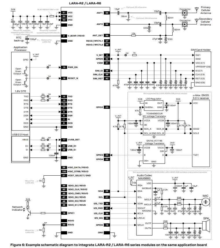
Appendix A Glossary
| Abbreviation | Definition |
| 2G | 2nd Generation Cellular Technology (GSM, GPRS, EGPRS) |
| 3G | 3rd Generation Cellular Technology (UMTS, HSDPA, HSUPA) |
| 3GPP | 3rd Generation Partnership Project |
| 8-PSK | 8 Phase-Shift Keying modulation |
| APAC | Asia-Pacific |
| AT | AT Command Interpreter Software Subsystem, or attention |
| AUX | Auxiliary |
| Cat | Category |
| CDMA | Code Division Multiple Access |
| CS | Coding Scheme |
| CSFB | Circuit-Switched-Fall-Back |
| CTS | Clear To Send |
| DCD | Data Carrier Detect |
| DCS | Digital Cellular System |
| DL | Down-Link (Reception) |
| DSR | Data Set Ready |
| DTLS | Datagram Transport Layer Security |
| DTR | Data Terminal Ready |
| EDGE | Enhanced Data rates for GSM Evolution (EGPRS) |
| eDRX | Extended Discontinuous Reception |
| EGPRS | Enhanced General Packet Radio Service (EDGE) |
| E-GSM | Extended GSM |
| EMEA | Europe, the Middle East and Africa |
| EMI | Electro-Magnetic Interference |
| ESD | Electro-Static Discharge |
| E-UTRA | Evolved Universal Terrestrial Radio Access |
| FDD | Frequency Division Duplex |
| FOAT | Firmware update Over AT commands |
| FOTA | Firmware update Over The Air |
| FTPS | File Transfer Protocol Secure |
| FW | Firmware |
| GMSK | Gaussian Minimum-Shift Keying modulation |
| GND | Ground |
| GNSS | Global Navigation Satellite System |
| GPIO | General Purpose Input Output |
| GPRS | General Packet Radio Service |
| GPS | Global Positioning System |
| GSM | Global System for Mobile communication |
| HSDPA | High Speed Downlink Packet Access |
| HSIC | High-Speed Inter-Chip USB interface |
| HSPA | High-Speed Packet Access |
| Abbreviation | Definition |
| HSUPA | High Speed Uplink Packet Access |
| HTTPS | HyperText Transfer Protocol Secure |
| I/O | Input/Output |
| I2C | Inter-Integrated Circuit interface |
| I2S | Inter IC Sound interface |
| IP | Internet Protocol |
| LED | Light Emitting Diode |
| LGA | Land Grid Array |
| LNA | Low Noise Amplifier |
| LPWA | Low Power Wide Area |
| LTE | Long Term Evolution |
| LwM2M | Open Mobile Alliance Lightweight Machine-to-Machine protocol |
| MCS | Modulation and Coding Scheme |
| MQTT | Message Queuing Telemetry Transport |
| PA | Power Amplifier |
| PCS | Personal Communications Service |
| PMU | Power Management Unit |
| PSM | Power Saving Mode |
| N.A. | Not Available / Not Applicable |
| RAT | Radio Access Technology |
| RF | Radio Frequency |
| RI | Ring Indication |
| Rx | Receiver |
| RTC | Real Time Clock |
| RTS | Request To Send |
| SAW | Surface Acoustic Wave |
| SDIO | Secure Digital Input Output |
| SIM | Subscriber Identification Module |
| SMS | Short Message Service |
| SPI | Serial Peripheral Interface |
| TCP | Transmission Control Protocol |
| TDD | Time Division Duplex |
| TLS | Transport Layer Security |
| TP | Test Point |
| Tx | Transmitter |
| UART | Universal Asynchronous Receiver-Transmitter |
| uCSP | u-blox Common Services Platform |
| UDP | User Datagram Protocol |
| uFOTA | u-blox Firmware update Over The Air |
| UL | Up-Link (Transmission) |
| UMTS | Universal Mobile Telecommunications System |
| URC | Unsolicited Result Code |
| USB | Universal Serial Bus |
| VoLTE | Voice over LTE |
- u-blox LARA-R2 series data sheet, UBX-16005783
- u-blox LARA-R2 series system integration manual, UBX-16010573
- u-blox nested design application note, UBX-16007243
- u-blox LARA-R6 series data sheet, UBX-21004391
- u-blox LARA-R6 series system integration manual, UBX-21010011
- u-blox AT commands manual, UBX-13002752
- u-blox LARA-R6 series AT commands manual, UBX-21046719
For regular updates to u-blox documentation and to receive product change notifications, register on our homepage (www.u-blox.com).
Revision history
| Revision | Date | Name | Comments |
| R01 | 29-Apr-2021 | sses | Initial release |
| R02 | 05-May-2022 | psca / sses | Added LARA-R6001D and LARA-R6401D. Some corrections and clarifications. |
Contact
- For complete contact information, visit us at www.u-blox.com.
- u-blox Offices
- North, Central and South America
- u-blox America, Inc.
- Phone: +1 703 483 3180
- Email: [email protected]
- Regional Office West Coast:
- Phone: +1 408 573 3640
- Email: [email protected]
Technical Support:
- Phone: +1 703 483 3185
- Email: [email protected]
- Headquarters
- Europe, Middle East, Africa
- u-blox AG
- Phone: +41 44 722 74 44
- Email: [email protected]
- Support: [email protected]
Asia, Australia, Pacific
- u-blox Singapore Pte. Ltd.
- Phone: +65 6734 3811
- Email: [email protected]
- Support: [email protected]
Regional Office Australia:
- Phone: +61 3 9566 7255
- Email: [email protected]
- Support: [email protected]
Regional Office China (Beijing):
- Phone: +86 10 68 133 545
- Email: [email protected]
- Support: [email protected]
Regional Office China (Chongqing):
- Phone: +86 23 6815 1588
- Email: [email protected]
- Support: [email protected]
Regional Office China (Shanghai):
- Phone: +86 21 6090 4832
- Email: [email protected]
- Support: [email protected]
Regional Office China (Shenzhen):
- Phone: +86 755 8627 1083
- Email: [email protected]
- Support: [email protected]
Regional Office India:
- Phone: +91 80 405 092 00
- Email: [email protected]
- Support: [email protected]
Regional Office Japan (Osaka):
- Phone: +81 6 6941 3660
- Email: [email protected]
- Support: [email protected]
Regional Office Japan (Tokyo):
- Phone: +81 3 5775 3850
- Email: [email protected]
- Support: [email protected]
Regional Office Korea:
- Phone: +82 2 542 0861
- Email: [email protected]
- Support: [email protected]
Regional Office Taiwan:
- Phone: +886 2 2657 1090
- Email: [email protected]
- Support: [email protected]


