u-blox SARA-U201 SARA Migration
 Abstract
This document provides hardware design guidelines to migrate between u-blox cellular modules based on SARA form factor. u-blox cellular modules having 2G, 3G, LTE-M, NB-IoT as dominant technology use this compact form factor to provide complete and cost-efficient solutions, specifically designed for IoT, offering multi-band data transmission.
Document information
| Title | SARA migration guide | |
| Subtitle | Guidelines to migrate between SARA modules | |
| Document type | Application note | |
| Document number | UBX-19045981 | |
| Revision and date | R08 | 02-Feb-2022 |
| Disclosure restriction | C1-Public | |
| Product status | Corresponding content status | |
| Functional sample | Draft | For functional testing. Revised and supplementary data will be published later. |
| In development / Prototype | Objective specification | Target values. Revised and supplementary data will be published later. |
| Engineering sample | Advance information | Data based on early testing. Revised and supplementary data will be published later. |
| Initial production | Early production information | Data from product verification. Revised and supplementary data may be published later. |
| Mass production / End of life | Production information | Document contains the final product specification. |
This document applies to the following products:
| Product name | Type number | Product status |
| SARA-R410M | SARA-R410M-02B-01 | End of life |
| SARA-R410M-02B-02 | End of life | |
| SARA-R410M-02B-03 | Initial production | |
| SARA-R410M-52B-01 | Mass production | |
| SARA-R410M-52B-02 | Mass production | |
| SARA-R410M-63B-00 | Obsolete | |
| SARA-R410M-63B-01 | Initial production | |
| SARA-R410M-73B-00 | Obsolete | |
| SARA-R410M-73B-01 | Obsolete | |
| SARA-R410M-73B-02 | Initial production | |
| SARA-R410M-83B-00 | Obsolete | |
| SARA-R410M-83B-01 | Initial production | |
| SARA-R412M | SARA-R412M-02B-01 | End of life |
| SARA-R412M-02B-02 | End of life | |
| SARA-R412M-02B-03 | Initial production | |
| SARA-R422 | SARA-R422-00B-00 | Initial production |
| SARA-R422S | SARA-R422S-00B-00 | Initial production |
| SARA-R422M8S | SARA-R422M8S-00B-00 | Initial production |
| SARA-R500S | SARA-R500S-00B-00 | Obsolete |
| SARA-R500S-00B-01 | Initial production | |
| SARA-R500S-01B-00 | Initial production | |
| SARA-R500S-61B-00 | Engineering sample | |
| SARA-R500S-71B-00 | Engineering sample | |
| SARA-R510S | SARA-R510S-00B-00 | Obsolete |
| SARA-R510S-00B-01 | Initial production | |
| SARA-R510S-01B-00 | Initial production | |
| SARA-R510S-61B-00 | Engineering sample | |
| SARA-R510S-71B-00 | Engineering sample |
| Product name | Type number | Product status |
| SARA-R510M8S | SARA-R510M8S-00B-00 | Obsolete |
| SARA-R510M8S-00B-01 | Initial production | |
| SARA-R510M8S-01B-00 | Initial production | |
| SARA-R510M8S-61B-00 | Engineering sample | |
| SARA-R510M8S-71B-00 | Engineering sample | |
| SARA-G300 | SARA-G300-00S-01 | Obsolete |
| SARA-G310 | SARA-G310-00S-01 | Obsolete |
| SARA-G340 | SARA-G340-00S-00 | Obsolete |
| SARA-G340-01S-00 | Obsolete | |
| SARA-G340-02S-00 | Obsolete | |
| SARA-G340-02S-01 | End of life | |
| SARA-G340 ATEX | SARA-G340-02X-00 | Obsolete |
| SARA-G340-02X-01 | Obsolete | |
| SARA-G350 | SARA-G350-00S-00 | Obsolete |
| SARA-G350-01S-00 | Obsolete | |
| SARA-G350-01B-00 | Obsolete | |
| SARA-G350-02S-00 | Obsolete | |
| SARA-G350-02S-01 | End of life | |
| SARA-G350 ATEX | SARA-G350-00X-00 | Obsolete |
| SARA-G350-02X-00 | Obsolete | |
| SARA-G350-02X-01 | End of life | |
| SARA-G350 Automotive | SARA-G350-02A-01 | End of life |
| SARA-G350-02A-02 | End of life | |
| SARA-G450 | SARA-G450-00C-00 | Obsolete |
| SARA-G450-00C-01 | Mass production | |
| SARA-G450-01C-00 | End of life | |
| SARA-G450-01C-01 | Mass production | |
| SARA-U201 | SARA-U201-03B-00 | Mass production |
| SARA-U201-63B-00 | Obsolete | |
| SARA-U201-63B-01 | Obsolete | |
| SARA-U201-63B-02 | Mass production | |
| SARA-U201-04B-00 | Mass production | |
| SARA-U201 ATEX | SARA-U201-03X-00 | Mass production |
| SARA-U201-04X-00 | Mass production | |
| SARA-U260 | SARA-U260-00S-01 | Obsolete |
| SARA-U260-00S-02 | End of life | |
| SARA-U260-03S-00 | Obsolete | |
| SARA-U260-03S-01 | Obsolete | |
| SARA-U270 | SARA-U270-00S-01 | Obsolete |
| SARA-U270-00S-02 | Obsolete | |
| SARA-U270-03S-00 | Obsolete | |
| SARA-U270-03S-01 | Obsolete | |
| SARA-U270-04B-00 | Obsolete | |
| SARA-U270-73S-00 | Obsolete | |
| SARA-U270-73S-01 | Obsolete | |
| SARA-U270-53S-00 | Obsolete | |
| SARA-U270-53S-01 | Obsolete | |
| SARA-U270-53S-02 | Obsolete | |
| SARA-U270 ATEX | SARA-U270-00X-00 | Obsolete |
| SARA-U270-00X-01 | Obsolete | |
| SARA-U280 | SARA-U280-00S-00 | Obsolete |
| SARA-U280-00S-01 | Obsolete | |
| SARA-U280-03S-00 | Obsolete | |
| SARA-U280-03S-01 | Obsolete | |
| Product name | Type number | Product status |
| SARA-U201 Automotive | SARA-U201-03A-00 | End of Life |
| SARA-U201-04A-00 | Obsolete | |
| SARA-U201-04A-01 | Mass Production | |
| SARA-U270 Automotive | SARA-U270-03A-00 | Obsolete |
| SARA-U270-03A-01 | Obsolete | |
| SARA-N310 | SARA-N310-00X-00 | End of Life |
| SARA-N310-00X-01 | Mass Production | |
| SARA-N200 | SARA-N200-02B-00 | Obsolete |
| SARA-N200-02B-01 | Obsolete | |
| SARA-N200-02B-02 | Obsolete | |
| SARA-N201 | SARA-N201-02B-00 | Obsolete |
| SARA-N201-02B-01 | End of life | |
| SARA-N210 | SARA-N210-02B-00 | Obsolete |
| SARA-N210-02B-01 | Obsolete | |
| SARA-N210-02B-02 | Obsolete | |
| SARA-N211 | SARA-N211-02X-00 | Obsolete |
| SARA-N211-02X-01 | Obsolete | |
| SARA-N211-02X-02 | End of life | |
| SARA-N280 | SARA-N280-02B-00 | Obsolete |
| SARA-N280-02B-01 | Obsolete |
u-blox or third parties may hold intellectual property rights in the products, names, logos and designs included in this document. Copying, reproduction, modification or disclosure to third parties of this document or any part thereof is only permitted with the express written permission of u-blox.
The information contained herein is provided “as is” and u-blox assumes no liability for its use. No warranty, either express or implied, is given, including but not limited to, with respect to the accuracy, correctness, reliability and fitness for a particular purpose of the information. This document may be revised by u-blox at any time without notice. For the most recent documents, visit www.u-blox.com.
SARA-R4/SARA-R5 modules description
u-blox SARA-R4 series LTE-M / NB-IoT / EGPRS and SARA-R5 series LTE-M / NB-IoT modules are ideal for IoT solutions, in the miniature SARA LGA form factor (26.0 x 16.0 mm, 96-pin).
They are easily integrated into compact designs and provide a seamless drop-in migration from other u-blox LPWA, GSM/GPRS, CDMA, UMTS/HSPA and LTE module families. They are form-factor compatible with the u-blox LISA, LARA and TOBY cellular module families and they are pin-to-pin compatible with the u-blox SARA-N, SARA-G and SARA-U cellular module families, thus maximizing customer investments, simplifying application design, and enabling a very short time-to-market.
Table 1 summarizes the main features and interfaces of SARA-R4 and SARA-R5 series modules.
With a discrete, hardware-based secure element and a lightweight pre-shared key management system, SARA-R5 series modules offer state-of-the-art security that is ideal for IoT applications and includes data encryption and decryption, zero touch provisioning, anti-cloning, and secure chip-to-chip communication. SARA-R4 and SARA-R5 series modules are the optimal choice for LPWA applications with low to medium data throughput rates, as well as devices that require long battery lifetimes, such as used in smart metering, smart cities, telematics, and connected health.
The modules support handover capability and deliver the technology necessary for use in applications such as vehicle, asset and people tracking where mobility is a pre-requisite. Other applications where the modules are well-suited include but are not limited to: smart home, security systems, industrial monitoring and control.
The modules support multi-band data communication over an extended operating temperature range of –40 to +85 °C, with extremely low power consumption, and with coverage enhancement for deeper range into buildings and basements (and underground with NB-IoT).
Table 2 summarizes cellular and GNSS characteristics of SARA-R4/R5 modules.
| Feature | SARA-R410M | SARA-R412M | SARA-R422 SARA-R422S SARA-R422M8S | SARA-R500S SARA-R510S SARA-R510M8S |
| Protocol stack | 3GPP release 13 | 3GPP release 13 | 3GPP release 14 | 3GPP release 14 |
| Cellular RAT | LTE Cat M1 Half-Duplex LTE Cat NB1 Half-Duplex 1,2 | LTE Cat M1 Half-Duplex LTE Cat NB1 Half-Duplex 2G GPRS / EGPRS | LTE Cat M1 Half-Duplex LTE Cat NB2 Half-Duplex 2G GPRS / EGPRS | LTE Cat M1 Half-Duplex LTE Cat NB2 Half-Duplex 3 |
| LTE FDD bands | Band 1 (2100 MHz) 1,5 | Band 2 (1900 MHz) | Band 1 (2100 MHz) | Band 1 (2100 MHz) |
| Band 2 (1900 MHz) 2,5 | Band 3 (1800 MHz) | Band 2 (1900 MHz) | Band 2 (1900 MHz) | |
| Band 3 (1800 MHz) 1 | Band 4 (1700 MHz) | Band 3 (1800 MHz) | Band 3 (1800 MHz) | |
| Band 4 (1700 MHz) 2,5 | Band 5 (850 MHz) | Band 4 (1700 MHz) | Band 4 (1700 MHz) | |
| Band 5 (850 MHz) | Band 8 (900 MHz) | Band 5 (850 MHz) | Band 5 (850 MHz) | |
| Band 8 (900 MHz) 1 | Band 12 (700 MHz) | Band 8 (900 MHz) | Band 8 (900 MHz) | |
| Band 12 (700 MHz) 2,5 | Band 13 (750 MHz) | Band 12 (700 MHz) | Band 12 (700 MHz) | |
| Band 13 (750 MHz) 2,5 | Band 20 (800 MHz) | Band 13 (750 MHz) | Band 13 (750 MHz) | |
| Band 18 (850 MHz) 1,2,5 | Band 26 (850 MHz) | Band 20 (800 MHz) | Band 18 (850 MHz) | |
| Band 19 (850 MHz) 1,5 | Band 28 (700 MHz) | Band 25 (1900 MHz) | Band 19 (850 MHz) | |
| Band 20 (800 MHz) 1,2 | Band 26 (850 MHz) | Band 20 (800 MHz) | ||
| Band 25 (1900 MHz) 1,2,4,5 | Band 28 (700 MHz) | Band 25 (1900 MHz) | ||
| Band 26 (850 MHz) 1,5 | Band 66 (1700 MHz) | Band 26 (850 MHz) | ||
| Band 28 (700 MHz) 1,2 | Band 85 (700 MHz) | Band 28 (700 MHz) | ||
| Band 66 (1700 MHz) | ||||
| Band 71 (600 MHz) | ||||
| Band 85 (700 MHz) | ||||
| 2G bands | GSM 850 MHz E-GSM 900 MHz DCS 1800 MHz PCS 1900 MHz | GSM 850 MHz E-GSM 900 MHz | ||
| Power class | LTE Cat M1 / NB16: Class 3 (23 dBm) | LTE Cat M1 / NB1: Class 3 (23 dBm) | LTE Cat M1 / NB2: Class 3 (23 dBm) | LTE Cat M1 / NB23: Class 3 (23 dBm) |
| 2G GMSK: GSM/E-GSM bands: Class 4 (33 dBm) DCS/PCS bands: Class 1 (30 dBm) | 2G GMSK: GSM/E-GSM bands: Class 4 (33 dBm) DCS/PCS bands: Class 1 (30 dBm) | |||
| 2G 8-PSK: GSM/E-GSM bands: Class E2 (27 dBm) DCS/PCS bands: Class E2 (26 dBm) | 2G 8-PSK: GSM/E-GSM bands: Class E2 (27 dBm) DCS/PCS bands: Class E2 (26 dBm) |
- Not supported by SARA-R410M-52B-01 or SARA-R410M-52B-02 product version
- Not supported by SARA-R410M-63B or SARA-R410M-73B product versions
- LTE Cat NB2 not supported by SARA-R500S-00B, SARA-R510S-00B, SARA-R510M8S-00B product versions
- Not supported in LTE Cat NB1 by SARA-R410M-02B-01, SARA-R410M-02B-02, or SARA-R410M-02B-03 product version
- Not supported by SARA-R410M-83B product version
- LTE Cat NB1 not supported by SARA-R410M-52B, SARA-R410M-63B, SARA-R410M-73B product versions
Feature SARA-R410M SARA-R412M SARA-R422 SARA-R422S SARA-R422M8S SARA-R500S SARA-R510S SARA-R510M8S Data rate LTE Cat M1:
up to 375 kbit/s UL up to 300 kbit/s DLLTE Cat M1:
up to 375 kbit/s UL up to 300 kbit/s DLLTE Cat M1:
up to 1119 kbit/s UL up to 588 kbit/s DLLTE Cat M1:
up to 1200 kbit/s UL up to 375 kbit/s DLLTE Cat NB17:
up to 62.5 kbit/s UL up to 27.2 kbit/s DLLTE Cat NB1:
up to 62.5 kbit/s UL up to 27.2 kbit/s DLLTE Cat NB2:
up to 158.5 kbit/s UL up to 127 kbit/s DLLTE Cat NB29:
up to 140 kbit/s UL up to 125 kbit/s DLGPRS multi-slot class 338 up to 85.6 kbit/s UL
up to 107 Kbit/s DLGPRS multi-slot class 338 up to 85.6 kbit/s UL
up to 107 kbit/s DLEGPRS multi-slot class 338 up to 236.8 kbit/s UL
up to 296.0 kbit/s DLEGPRS multi-slot class 338 up to 236.8 kbit/s UL
up to 296.0 kbit/s DLGNSS receiver SARA-R422M8S only: SARA-R510M8S only: 72-channel
u-blox M8 engine72-channel
u-blox M8 engineGPS L1C/A SBAS L1C/A QZSS L1C/A QZSS L1-SAIF GLONASS L10F
BeiDou B1I Galileo E1B/CGPS L1C/A SBAS L1C/A QZSS L1C/A QZSS L1-SAIF GLONASS L10F
BeiDou B1I Galileo E1B/C - LTE Cat NB1 not supported by SARA-R410M-52B, SARA-R410M-63B, SARA-R410M-73B product versions
- GPRS/EGPRS multi-slot class 33 implies a maximum of 5 slots in downlink and 4 slots in uplink, with 6 slots in total
- LTE Cat NB2 not supported by SARA-R500S-00B, SARA-R510S-00B, SARA-R510M8S-00B product versions
SARA-N2/SARA-N3 modules description
SARA-N2 and SARA-N3 series modules are NB-IoT solutions in the miniature SARA LGA form factor (26.0 x 16.0 mm, 96-pin), offering LTE Cat NB1 / NB2 data communication over an extended operating temperature range of –40 to +85 °C, with extremely low power consumption.
The SARA-N2 series includes four variants supporting single-band NB-IoT data communication for Europe, China, APAC and South America, plus a dual-band variant mainly designed for Europe.
The SARA-N3 series offers multi-band NB-IoT data communication enabling multi-regional coverage, and they introduce several new functionalities for NB-IoT products, including features like TCP, MQTT, DTLS, SSL/TLS, LwM2M, HTTP(S) and many others.
SARA-N2 and SARA-N3 modules are ideally suited to battery-powered IoT applications characterized by occasional communications of small amounts of data.
The modules are the optimal choice for IoT devices designed to operate in locations with very limited coverage and requiring low energy consumption to permit a very long operating life with the primary batteries. Examples of applications include and are not limited to: smart grids, smart metering, telematics, street lighting, environmental monitoring and control, security and asset tracking.
Table 3 describes a summary of interfaces and features provided by SARA-N2 and SARA-N3 modules. Table 4 summarizes cellular radio access technology characteristics of SARA-N2 / SARA-N3 modules.
| Item | SARA-N2 series | SARA-N31010 |
| Protocol stack | 3GPP Release 13 | 3GPP Release 1411 |
| Radio Access Technology | LTE Category NB1 Half-Duplex Single-tone Single HARQ process eDRX Power Saving Mode Coverage enhancement A and B | LTE Category NB2 Half-Duplex Multi-tone Two HARQ process eDRX Power Saving Mode Coverage enhancement A and B |
| Operating band | SARA-N200:
| Band 3 (1800 MHz) Band 5 (850 MHz) Band 8 (900 MHz) Band 20 (800 MHz) Band 28 (700 MHz) |
| Power class | Class 3 (23 dBm)12 | Class 3 (23 dBm)12 |
| Deployment mode | In-Band Guard-Band Standalone | In-Band Guard-Band Standalone |
| Radio link data rate | Up to 31.25 kb/s UL Up to 27.2 kb/s DL | Up to 140 kb/s UL Up to 125 kb/s DL |
- 10 Additional bands (1, 2, 4, 12, 13, 18, 19, 26, 66, 71, 85) available in future FW versions
- 11 Key subset of features
- 12 Configurable to other power class by AT command
Migration between SARA modules
Overview
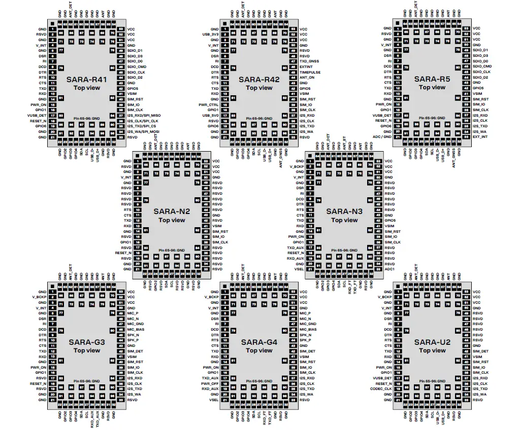
The u-blox SARA form factor (26.0 x 16.0 mm, 96-pin LGA) includes the following series of modules, with compatible pin assignments as described in Figure 1, so that the modules can be alternatively mounted on a single application PCB using exactly the same copper, solder resist and paste mask:
- SARA-R41 series modules supporting LTE Cat M1, LTE Cat NB1 and 2G radio access technologies
- SARA-R42 series modules supporting LTE Cat M1, LTE Cat NB2 and 2G radio access technologies
- SARA-R5 series modules supporting LTE Cat M1 and LTE Cat NB2 radio access technologies
- SARA-N2 series modules supporting LTE Cat NB1 radio access technology
- SARA-N3 series modules supporting LTE Cat NB2 radio access technology
- SARA-G3 series modules supporting 2G radio access technology
- SARA-G4 series modules supporting 2G radio access technology
- SARA-U2 series modules supporting 3G and 2G radio access technologies

The SARA modules are also form-factor compatible with the u-blox LARA, LISA, and TOBY cellular module families. Although each has a different form factor, the footprints for the TOBY, LISA, LARA, and SARA modules have been developed to ensure layout compatibility.
With the u-blox “nested design” solution, any TOBY, LISA, LARA, or SARA module can be alternatively mounted on the same space of a single “nested” application board as described in Figure 2. Guidelines to implement a nested application board, description of the u-blox reference nested design and comparison between TOBY, LISA, LARA and SARA modules are provided in the nested design application note [10].
Figure 2: Cellular modules’ layout compatibility: all modules can be mounted on the same nested footprint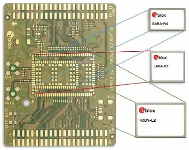 Table 5 summarizes the main interfaces provided by SARA modules:
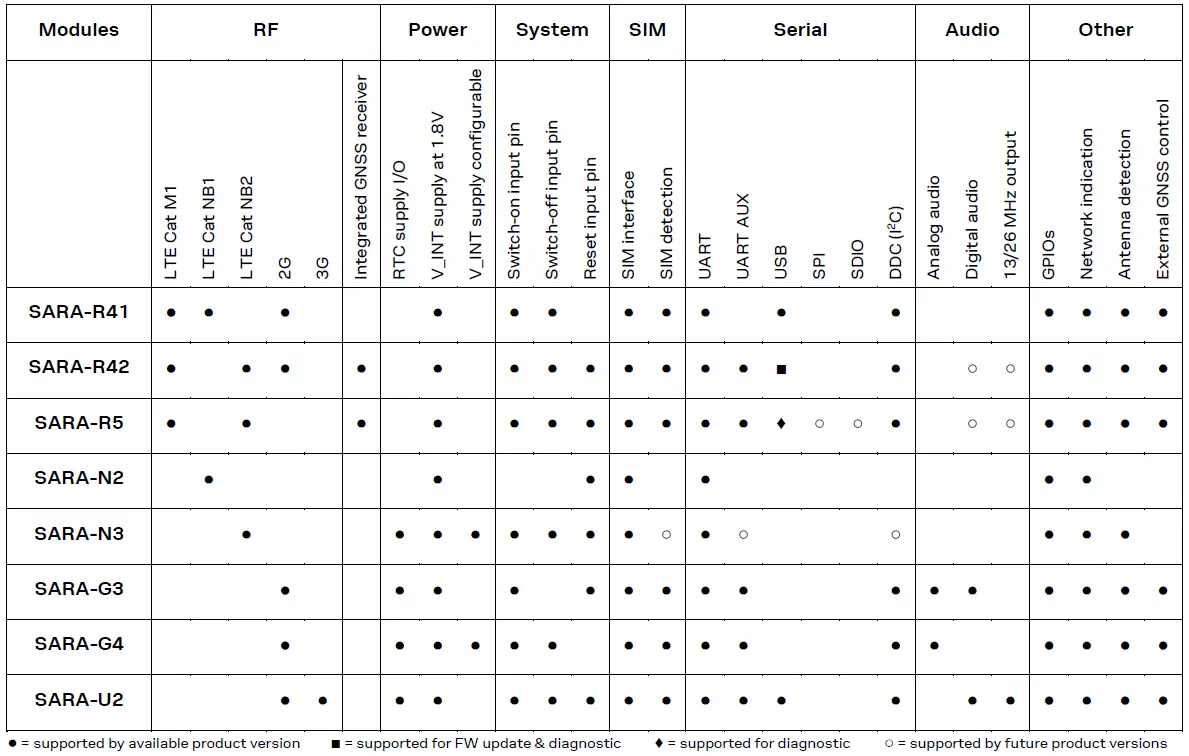 Figure 3 summarizes the frequency ranges of the SARA modules’ operating bands.
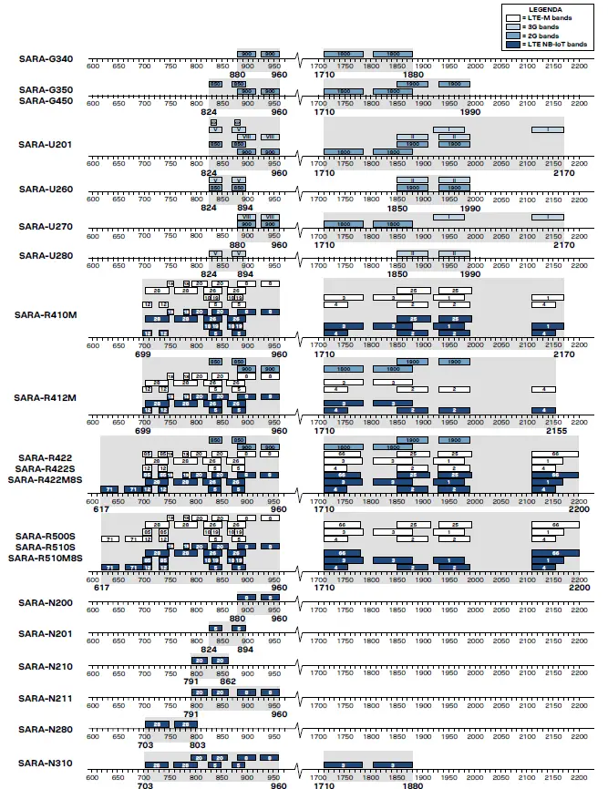
Pin-out comparison between SARA modules
Table 6 shows a pin-out comparison between the SARA-R4, SARA-R5, SARA-N2, SARA-N3, SARA-G3, SARA-G4, and SARA-U2 modules.
| No | SARA-R41 series | SARA-R42 series | SARA-R5 series | SARA-N2 series | SARA-N3 series | SARA-G3 series | SARA-G4 series | SARA-U2 series |
| 1 | GND | GND | GND | GND | GND | GND | GND | GND |
| Ground | Ground | Ground | Ground | Ground | Ground | Ground | Ground | |
| 2 | RSVD | USB_3V3 | RSVD | RSVD | V_BCKP | V_BCKP | V_BCKP | V_BCKP |
| Reserved | USB 3V3 supply Input TestPoint recommended | Reserved | Reserved | RTC supply I/O | RTC supply I/O | RTC supply I/O | RTC supply I/O | |
| 3 | GND | GND | GND | GND | GND | GND | GND | GND |
| Ground | Ground | Ground | Ground | Ground | Ground | Ground | Ground | |
| 4 | V_INT | V_INT | V_INT | V_INT | V_INT | V_INT | V_INT | V_INT |
| Supply output: 1.8 V typ ON when SARA is on TestPoint recommended | Supply output: 1.8 V typ ON when SARA is on TestPoint recommended | Supply output: 1.8 V typ ON when SARA is on TestPoint recommended | Supply output: 1.8 V typ ON when radio is on TestPoint recommended | Supply output: 1.8 V typ / 2.8 V typ ON when SARA is on Voltage value set by VSEL TestPoint recommended | Supply output: 1.8 V typ ON when SARA is on TestPoint recommended | Supply output: 1.8 V typ / 3.0 V typ ON when SARA is on Voltage value set by VSEL TestPoint recommended | Supply output: 1.8 V typ ON when SARA is on TestPoint recommended | |
| 5 | GND | GND | GND | GND | GND | GND | GND | GND |
| Ground | Ground | Ground | Ground | Ground | Ground | Ground | Ground | |
| 6 | DSR | DSR | DSR | RSVD | DSR | DSR | DSR | DSR |
| UART DSR output | UART DSR output | UART DSR output | Reserved | UART DSR output13 | UART DSR output | UART DSR output | UART DSR output | |
| V_INT level (1.8 V) | V_INT level (1.8 V) | V_INT level (1.8 V) | V_INT level (1.8 / 2.8 V) | V_INT level (1.8 V) | V_INT level (1.8 / 3.0 V) | V_INT level (1.8 V) | ||
| Driver strength: 2 mA | Driver strength: 2 mA | Driver strength: 5 mA | Driver strength: 6 mA | Driver strength: 3 mA | Driver strength: 1 mA | |||
| Also RTS for 2nd UART | Also RTS for 2nd UART | |||||||
| 7 | RI | RI | RI | RSVD | RI | RI | RI | RI |
| UART RI output | UART RI output | UART RI output | Reserved | UART RI output | UART RI output | UART RI output | UART RI output | |
| V_INT level (1.8 V) | V_INT level (1.8 V) | V_INT level (1.8 V) | V_INT level (1.8 / 2.8 V) | V_INT level (1.8 V) | V_INT level (1.8 / 3.0 V) | V_INT level (1.8 V) | ||
| Driver strength: 2 mA | Driver strength: 2 mA | Driver strength: 5 mA | Driver strength: 3 mA | Driver strength: 6 mA | Driver strength: 3 mA | Driver strength: 2 mA | ||
| Also CTS for 2nd UART | Also CTS for 2nd UART | Configurable as GPIO | ||||||
| 8 | DCD | DCD | DCD | RSVD | DCD | DCD | DCD | DCD |
| UART DCD output | UART DCD output | UART DCD output | Reserved | UART DCD output13 | UART DCD output | UART DCD output | UART DCD output | |
| V_INT level (1.8 V) | V_INT level (1.8 V) | V_INT level (1.8 V) | V_INT level (1.8 / 2.8 V) | V_INT level (1.8 V) | V_INT level (1.8 / 3.0 V) | V_INT level (1.8 V) | ||
| Driver strength: 2 mA | Driver strength: 2 mA | Driver strength: 5 mA | Driver strength: 6 mA | Driver strength: 3 mA | Driver strength: 2 mA | |||
| Also RXD for 2nd UART | Also RXD for 2nd UART Test Point recommended |
| No | SARA-R41 series | SARA-R42 series | SARA-R5 series | SARA-N2 series | SARA-N3 series | SARA-G3 series | SARA-G4 series | SARA-U2 series |
| 9 | DTR | DTR | DTR | RSVD | DTR | DTR | DTR | DTR |
| UART DTR input V_INT level (1.8 V) Internal pull-up: ~100 kΩ Set low for URCs/Greeting | UART DTR input V_INT level (1.8 V) Internal pull-up: ~100 kΩ Set low for greeting text Also TXD for 2nd UART | UART DTR input V_INT level (1.8 V) Internal pull-up: ~56 kΩ Set low for greeting text Also TXD for 2nd UART TestPoint recommended | Reserved | UART DTR input14 V_INT level (1.8 / 2.8 V) | UART DTR input V_INT level (1.8 V) Internal pull-up: ~33 kΩ | UART DTR input V_INT level (1.8 / 3.0 V) Internal pull-up: ~166 kΩ | UART DTR input V_INT level (1.8 V) Internal pull-up: ~14 kΩ Set low for greeting text | |
| 10 | RTS | RTS | RTS | RTS | RTS | RTS | RTS | RTS |
| UART RTS input V_INT level (1.8 V) Internal pull-up: ~100 kΩ Must be low to use UART on “00”, “01” versions | UART RTS input V_INT level (1.8 V) Internal pull-up: ~100 kΩ | UART RTS input V_INT level (1.8 V) Internal pull-up: ~56 kΩ | UART RTS input15 VCC level (3.6 V typ.) Internal pull-up: ~78 kΩ | UART RTS input V_INT level (1.8 / 2.8 V) Internal pull-up: ~171 kΩ Configurable as GPIO | UART RTS input V_INT level (1.8 V) Internal pull-up:~58 kΩ | UART RTS input V_INT level (1.8 / 3.0 V) Internal pull-up: ~166 kΩ | UART RTS input V_INT level (1.8 V) Internal pull-up: ~8 kΩ | |
| 11 | CTS | CTS | CTS | CTS | CTS | CTS | CTS | CTS |
| UART CTS output V_INT level (1.8 V) Driver strength: 2 mA | UART CTS output V_INT level (1.8 V) Driver strength: 2 mA | UART CTS output V_INT level (1.8 V) Driver strength: 5 mA | UART CTS output15 VCC level (3.6 V typ.) Driver strength: 1 mA Configurable as RI or Network Indicator | UART CTS output V_INT level (1.8 / 2.8 V) Driver strength: 3 mA Configurable as GPIO or Network Indicator | UART CTS output V_INT level (1.8 V) Driver strength: 6 mA | UART CTS output V_INT level (1.8 / 3.0 V) Driver strength: 3 mA | UART CTS output V_INT level (1.8 V) Driver strength: 6 mA | |
| 12 | TXD | TXD | TXD | TXD | TXD | TXD | TXD | TXD |
| UART data input V_INT level (1.8 V) Internal PU/PD ~100 kΩ | UART data input V_INT level (1.8 V) Internal pull-up ~100 kΩ | UART data input V_INT level (1.8 V) Internal pull-up: ~56 kΩ TestPoint recommended | UART data input VCC level (3.6 V typ.) No internal pull-up/down TestPoint recommended | UART data input V_INT level (1.8 / 2.8 V) Internal pull-up: ~171 kΩ | UART data input V_INT level (1.8 V) Internal pull-up: ~18 kΩ | UART data input V_INT level (1.8 / 3.0 V) Internal pull-up: ~166 kΩ | UART data input V_INT level (1.8 V) Internal pull-up: ~8 kΩ | |
| 13 | RXD | RXD | RXD | RXD | RXD | RXD | RXD | RXD |
| UART data output V_INT level (1.8 V) Driver strength: 2 mA | UART data output V_INT level (1.8 V) Driver strength: 2 mA | UART data output V_INT level (1.8 V) Driver strength: 5 mA TestPoint recommended | UART data output VCC level (3.6 V typ.) Driver strength: 1 mA TestPoint recommended | UART data output V_INT level (1.8 / 2.8 V) Driver strength: 3 mA | UART data output V_INT level (1.8 V) Driver strength: 6 mA | UART data output V_INT level (1.8 / 3.0 V) Driver strength: 3 mA | UART data output V_INT level (1.8 V) Driver strength: 6 mA | |
| 14 | GND | GND | GND | GND | GND | GND | GND | GND |
| Ground | Ground | Ground | Ground | Ground | Ground | Ground | Ground | |
| 15 | PWR_ON | PWR_CTRL | PWR_ON | RSVD | PWR_ON | PWR_ON | PWR_ON | PWR_ON |
| Power-on/off input Internal pull-up: ~200 kΩ L-level: -0.30 ÷ 0.35 V ON L-level time: 0.15 s min – 3.2 s max OFF L-level pulse time: 1.5 s min TestPoint recommended | Power-on/off / reset input Internal pull-up L-level: -0.30 ÷ 0.35 V ON L-level pulse time: 0.01 s min – 1.7 s max OFF L-level pulse time: 1.5 s min – 14 s max Reset L-level pulse time: 16 s min TestPoint recommended | Power-on/off input Internal pull-up: ~10 kΩ L-level: -0.30 ÷ 0.30 V ON L-level time: 1 s min – 2 s max OFF L-level pulse time: 1.5 s min – 2.5 s max TestPoint recommended | Reserved | Power-on/off input Internal pull-up: ~90 kΩ L-level: 0.00 ÷ 0.20 V ON L-level pulse time: 1 s min – 2.5 s max OFF L-level pulse time: 2.5 s min TestPoint recommended | Power-on input No internal pull-up L-level: -0.10 ÷ 0.65 V ON L-level time: 5 ms min OFF L-level pulse time: Not Available TestPoint recommended | Power-on input Internal pull-up: ~28 kΩ L-level: 0.00 ÷ 0.30 V ON L-level time: 2 s min OFF L-level time: Not Available TestPoint recommended | Power-on/off input No internal pull-up L-level: -0.30 ÷ 0.65 V ON L-level pulse time: 50 µs min / 80 µs max OFF L-level pulse time: 1 s min TestPoint recommended |
| No | SARA-R41 series | SARA-R42 series | SARA-R5 series | SARA-N2 series | SARA-N3 series | SARA-G3 series | SARA-G4 series | SARA-U2 series |
| 16 | GPIO1 | GPIO1 | GPIO1 | GPIO1 | GPIO1 | GPIO1 | GPIO1 | GPIO1 |
| GPIO V_INT level (1.8 V) Driver strength: 2 mA | GPIO V_INT level (1.8 V) Driver strength: 2 mA | GPIO V_INT level (1.8 V) Driver strength: 5 mA | Trace data output V_INT level (1.8 V) Driver strength: 1 mA TestPoint recommended | GPIO V_INT level (1.8 / 2.8 V) Driver strength: 3 mA | GPIO V_INT level (1.8 V) Driver strength: 6 mA | GPIO V_INT level (1.8 / 3.0 V) Driver strength: 3 mA | GPIO V_INT level (1.8 V) Driver strength: 6 mA | |
| 17 | VUSB_DET | USB_5V0 | VUSB_DET | RSVD | TXD_AUX | RSVD | TXD_AUX | VUSB_DET |
| 5 V, USB detect input TestPoint recommended | USB 5V0 supply Input TestPoint recommended | 5 V, USB detect input TestPoint recommended | Reserved | AUX UART data input16 V_INT level (1.8 / 2.8 V) | Reserved | AUX UART data input17 V_INT level (1.8 / 3.0 V) Internal pull-up: ~166 kΩ | 5 V, USB detect input TestPoint recommended | |
| 18 | RESET_N | RSVD | RESET_N | RESET_N | RESET_N | RESET_N | PWR_OFF | RESET_N |
| Shutdown input Internal pull-up: ~37 kΩ L-level: -0.30 ÷ 0.63 V H-level: 1.17 ÷ 2.10 V It triggers shutdown of the whole module when set low or toggled. TestPoint recommended | Reserved | Reset input Internal pull-up: ~56 kΩ L-level: -0.30 ÷ 0.50 V H-level: 1.3 ÷ 2.1 V It triggers module reboot when toggled, without PMU shutdown when low. TestPoint recommended | Reset input Internal pull-up: ~78 kΩ L-level: 0 ÷ 0.36*VCC H-level: 0.52*VCC ÷ VCC It triggers module reboot when toggled, without PMU shutdown when low. TestPoint recommended | Reset shutdown input Internal pull-up: ~70 kΩ L-level: 0.00 ÷ 0.20 V H-level: 0.90 ÷ 1.10 V It triggers module reboot when toggled, with PMU shutdown when low. TestPoint recommended | Reset input Internal diode & pull-up L-level: -0.10 ÷ 0.15 V H-level: 1.40 ÷ 4.50 V It triggers module reboot when toggled, without PMU shutdown when low. TestPoint recommended | Shutdown input Internal diode L-level: 0.00 ÷ 0.10 V H-level: 1.20 ÷ 1.50 V It triggers shutdown of the whole module when set low or toggled. TestPoint recommended | Reset shutdown input Internal pull-up: 10 kΩ L-level: -0.30 ÷ 0.51 V H-level: 1.32 ÷ 2.01 V It triggers module reboot when toggled, with PMU shutdown when low. TestPoint recommended | |
| 19 | GPIO6 | GPIO6 | GPIO6 | RSVD | RXD_AUX | RSVD | RXD_AUX | CODEC_CLK |
| GPIO V_INT level (1.8 V) Driver strength: 2 mA | GPIO V_INT level (1.8 V) Driver strength: 2 mA | GPIO V_INT level (1.8 V) Driver strength: 5 mA | Reserved | AUX UART data output16 V_INT level (1.8 / 2.8 V) | Reserved | AUX UART data output17 V_INT level (1.8 / 3.0 V) Driver strength: 3 mA | 13 or 26 MHz output V_INT level (1.8 V) Driver strength: 4 mA | |
| 20 | GND | GND | GND | GND | GND | GND | GND | GND |
| Ground | Ground | Ground | Ground | Ground | Ground | Ground | Ground | |
| 21 | GND | GND | GND / ADC | GND | VSEL | GND | VSEL | GND |
| Ground | Ground | “00B” product version: Ground “x1B” product versions: 12-bit ADC input, which can also be grounded | Ground | V_INT voltage selection VSEL connected to GND: V_INT = 1.8 V VSEL unconnected: V_INT = 2.8 V | Ground | V_INT voltage selection VSEL connected to GND: V_INT = 1.8 V VSEL unconnected: V_INT = 3.0 V | Ground | |
| 22 | GND | GND | GND | GND | GND | GND | GND | GND |
| Ground | Ground | Ground | Ground | Ground | Ground | Ground | Ground | |
| 23 | GPIO2 | GPIO2 | GPIO2 | RSVD | GPIO2 | GPIO2 | GPIO2 | GPIO2 |
| GPIO V_INT level (1.8 V) Driver strength: 2 mA | GPIO V_INT level (1.8 V) Driver strength: 2 mA | GPIO V_INT level (1.8 V) Driver strength: 5 mA | Reserved | GPIO V_INT level (1.8 / 2.8 V) Driver strength: 3 mA | GPIO V_INT level (1.8 V) Driver strength: 6 mA | GPIO V_INT level (1.8 / 3.0 V) Driver strength: 3 mA | GPIO V_INT level (1.8 V) Driver strength: 6 mA | |
| 24 | GPIO3 | GPIO3 | GPIO3 | GPIO2 | GPIO3 | GPIO3 | GPIO3 | GPIO3 |
| GPIO V_INT level (1.8 V) Driver strength: 2 mA | GPIO V_INT level (1.8 V) Driver strength: 2 mA | GPIO V_INT level (1.8 V) Driver strength: 5 mA | GPIO1 V_INT level (1.8 V) Driver strength: 1 mA | GPIO V_INT level (1.8 / 2.8 V) Driver strength: 3 mA | GPIO V_INT level (1.8 V) Driver strength: 5 mA | GPIO V_INT level (1.8 / 3.0 V) Driver strength: 3 mA | GPIO V_INT level (1.8 V) Driver strength: 6 mA |
| No | SARA-R41 series | SARA-R42 series | SARA-R5 series | SARA-N2 series | SARA-N3 series | SARA-G3 series | SARA-G4 series | SARA-U2 series |
| 25 | GPIO4 | GPIO4 | GPIO4 | RSVD | GPIO4 | GPIO4 | GPIO4 | GPIO4 |
| GPIO V_INT level (1.8 V) Driver strength: 2 mA | GPIO V_INT level (1.8 V) Driver strength: 2 mA | GPIO V_INT level (1.8 V) Driver strength: 5 mA | Reserved | GPIO V_INT level (1.8 / 2.8 V) Driver strength: 3 mA | GPIO V_INT level (1.8 V) Driver strength: 6 mA | GPIO V_INT level (1.8 / 3.0 V) Driver strength: 3 mA | GPIO V_INT level (1.8 V) Driver strength: 6 mA | |
| 26 | SDA | SDA | SDA | SDA | SDA | SDA | SDA | SDA |
| I2C data19 | I2C data | I2C data | I2C data20 | I2C data21 | I2C data | I2C data22 | I2C data / AUX UART input | |
| V_INT level (1.8 V) | V_INT level (1.8 V) | V_INT level (1.8 V) | V_INT level (1.8 V) | V_INT level (1.8 / 2.8 V) | V_INT level (1.8 V) | V_INT level (1.8 / 3.0 V) | V_INT level (1.8 V) | |
| Open drain | Open drain | Open drain | Open drain | Open drain | Open drain | Open drain | Open drain | |
| Internal pull-up: 2.2 kΩ | Internal pull-up: 2.2 kΩ | Internal active pull-up | No internal pull-up | Internal pull-up: 10 kΩ | No internal pull-up | No internal pull-up | No internal pull-up | |
| 27 | SCL | SCL | SCL | SCL | SCL | SCL | SCL | SCL |
| I2C clock19 | I2C clock | I2C clock | I2C clock20 | I2C clock21 | I2C clock | I2C clock22 | I2C clock / AUX UART out | |
| V_INT level (1.8 V) | V_INT level (1.8 V) | V_INT level (1.8 V) | V_INT level (1.8 V) | V_INT level (1.8 / 2.8 V) | V_INT level (1.8 V) | V_INT level (1.8 / 3.0 V) | V_INT level (1.8 V) | |
| Open drain | Open drain | Open drain | Open drain | Open drain | Open drain | Open drain | Open drain | |
| Internal pull-up: 2.2 kΩ | Internal pull-up: 2.2 kΩ | Internal active pull-up | No internal pull-up | Internal pull-up: 10 kΩ | No internal pull-up | No internal pull-up | No internal pull-up | |
| 28 | USB_D- | USB_D- | USB_D- | RSVD | RXD_FT | RXD_AUX | RXD_FT | USB_D- |
| USB data I/O (D-) | USB data I/O (D-) | USB data I/O (D-) | Reserved | FW update & Trace output | AUX UART data output | FW update & Trace output | USB data I/O (D-) | |
| High-speed USB 2.0 TestPoint recommended | High-speed USB 2.0, only for FW update / diagnostic | High-speed USB 2.0, only for diagnostic | V_INT level (1.8 / 2.8 V) Driver strength: 3 mA | V_INT level (1.8 V) Driver strength: 5 mA | V_INT level (1.8 / 3.0 V) Driver strength: 3 mA | High-speed USB 2.0 TestPoint recommended | ||
| TestPoint recommended | TestPoint recommended | TestPoint recommended | TestPoint recommended | TestPoint recommended | ||||
| 29 | USB_D+ | USB_D+ | USB_D+ | RSVD | TXD_FT | TXD_AUX | TXD_FT | USB_D+ |
| USB data I/O (D+) | USB data I/O (D+) | USB data I/O (D+) | Reserved | FW update & Trace input | AUX UART data input | FW update & Trace input | USB data I/O (D+) | |
| High-speed USB 2.0 TestPoint recommended | High-speed USB 2.0, only for FW update / diagnostic | High-speed USB 2.0, only for diagnostic | V_INT level (1.8 / 2.8 V) Internal pull-up: ~171 kΩ | V_INT level (1.8 V) Internal pull-up:~18 kΩ | V_INT level (1.8 / 3.0 V) Internal pull-up: ~166 kΩ | High-speed USB 2.0 TestPoint recommended | ||
| TestPoint recommended | TestPoint recommended | TestPoint recommended | TestPoint recommended | TestPoint recommended | ||||
| 30 | GND | GND | GND | GND | GND | GND | GND | GND |
| Ground | Ground | Ground | Ground | Ground | Ground | Ground | Ground | |
| 31 | RSVD | ANT_GNSS | ANT_GNSS | RSVD | RSVD | RSVD | RSVD | RSVD |
| Reserved | GNSS RF input23 | GNSS RF input24 | Reserved | Reserved | Reserved | Reserved | Reserved | |
| 32 | GND | GND | GND | GND | GND | GND | GND | GND |
| Ground | Ground | Ground | Ground | Ground | Ground | Ground | Ground | |
| 33 | RSVD | RSVD | EXT_INT | RSVD | ADC1 | RSVD | RSVD | RSVD |
| Reserved It can be grounded | Reserved TestPoint recommended | External interrupt It can be grounded | Reserved It can be grounded | ADC input It can be grounded | Reserved It must be grounded | Reserved It can be grounded | Reserved It must be grounded |
| No | SARA-R41 series | SARA-R42 series | SARA-R5 series | SARA-N2 series | SARA-N3 series | SARA-G3 series | SARA-G4 series | SARA-U2 series |
| 34 | I2S_WA / SPI_MOSI | I2S_WA | I2S_WA | RSVD | RSVD | I2S_WA | I2S_WA | I2S_WA |
| I2S W.A.25 / SPI MOSI25 | I2S Word Alignment26 | I2S Word Alignment27 | Reserved | Reserved | I2S Word Alignment | Not supported | I2S Word Alignment | |
| V_INT level (1.8 V) | V_INT level (1.8 V) | V_INT level (1.8 V) | V_INT level (1.8 V) | V_INT level (1.8 V) | ||||
| Driver strength: 2 mA | Driver strength: 2 mA | Configurable as antenna dynamic tuner | Driver strength: 6 mA | Driver strength: 2 mA Configurable as GPIO | ||||
| 35 | I2S_TXD / SPI_CS | I2S_TXD | I2S_TXD | RSVD | RSVD | I2S_TXD | I2S_TXD | I2S_TXD |
| I2S out25 / SPI CS25 | I2S data output26 | I2S data output27 | Reserved | Reserved | I2S data output | Not supported | I2S data output | |
| V_INT level (1.8 V) | V_INT level (1.8 V) | V_INT level (1.8 V) | V_INT level (1.8 V) | V_INT level (1.8 V) | ||||
| Driver strength: 2 mA | Driver strength: 2 mA | Configurable as antenna dynamic tuner | Driver strength: 5 mA | Driver strength: 2 mA Configurable as GPIO | ||||
| 36 | I2S_CLK / SPI_CLK | I2S_CLK | I2S_CLK | RSVD | RSVD | I2S_CLK | I2S_CLK | I2S_CLK |
| I2S clock25 / SPI clock25 | I2S clock26 | I2S clock27 | Reserved | Reserved | I2S clock | Not supported | I2S clock | |
| V_INT level (1.8 V) | V_INT level (1.8 V) | V_INT level (1.8 V) | V_INT level (1.8 V) | V_INT level (1.8 V) | ||||
| Driver strength: 2 mA | Driver strength: 2 mA | GEOFENCE 1.8 V PIO15 of the internal UBX-M8 GNSS on SARA-R510M8S-x1B | Driver strength: 5 mA | Driver strength: 2 mA Configurable as GPIO | ||||
| 37 | I2S_RXD / SPI_MISO | I2S_RXD | I2S_RXD | RSVD | RSVD | I2S_RXD | I2S_RXD | I2S_RXD |
| I2S input25 / SPI MISO25 | I2S input26 | I2S data input27 | Reserved | Reserved | I2S data input | Not supported | I2S data input | |
| V_INT level (1.8 V) | V_INT level (1.8 V) | V_INT level (1.8 V) | V_INT level (1.8 V) | V_INT level (1.8 V) | ||||
| ANT_ON 1.8 V PIO16 of the internal UBX-M8 GNSS on SARA-R510M8S-x1B | Internal pull-down: ~18 kΩ | Internal pull-down: ~8 kΩ Configurable as GPIO | ||||||
| 38 | SIM_CLK | SIM_CLK | SIM_CLK | SIM_CLK | SIM_CLK | SIM_CLK | SIM_CLK | SIM_CLK |
| 1.8 V / 3 V SIM clock | 1.8 V SIM clock | 1.8 V / 3 V SIM clock | 1.8 V SIM clock | 1.8 V / 3 V SIM clock | 1.8 V / 3 V SIM clock | 1.8 V / 3 V SIM clock | 1.8 V / 3 V SIM clock | |
| 39 | SIM_IO | SIM_IO | SIM_IO | SIM_IO | SIM_IO | SIM_IO | SIM_IO | SIM_IO |
| 1.8 V / 3 V SIM data I/O Internal pull-up: 4.7 kΩ | 1.8 V SIM data I/O Internal pull-up: 4.7 kΩ | 1.8 V / 3 V SIM data I/O Internal pull-up: 4.7 kΩ | 1.8 V SIM data I/O Internal pull-up: 4.7 kΩ | 1.8 V / 3 V SIM data I/O Internal pull-up: 4.7 kΩ | 1.8 V / 3 V SIM data I/O Internal pull-up: 4.7 kΩ | 1.8 V / 3 V SIM data I/O Internal pull-up: 4.7 kΩ | 1.8 V / 3 V SIM data I/O Internal pull-up: 4.7 kΩ | |
| 40 | SIM_RST | SIM_RST | SIM_RST | SIM_RST | SIM_RST | SIM_RST | SIM_RST | SIM_RST |
| 1.8 V / 3 V SIM reset | 1.8 V SIM reset | 1.8 V / 3 V SIM reset | 1.8 V SIM reset | 1.8 V / 3 V SIM reset | 1.8 V / 3 V SIM reset | 1.8 V / 3 V SIM reset | 1.8 V / 3 V SIM reset | |
| 41 | VSIM | VSIM | VSIM | VSIM | VSIM | VSIM | VSIM | VSIM |
| 1.8 V / 3 V SIM supply | 1.8 V SIM supply | 1.8 V / 3 V SIM supply | 1.8 V SIM supply | 1.8 V / 3 V SIM supply | 1.8 V / 3 V SIM supply | 1.8 V / 3 V SIM supply | 1.8 V / 3 V SIM supply | |
| 42 | GPIO5 | GPIO5 | GPIO5 | RSVD | GPIO5 | SIM_DET | SIM_DET | SIM_DET |
| GPIO / SIM detection input V_INT level (1.8 V) Driver strength: 2 mA | GPIO / SIM detection input V_INT level (1.8 V) Driver strength: 2 mA | GPIO / SIM detection input V_INT level (1.8 V) Driver strength: 5 mA | Reserved | SIM detection28 / GPIO V_INT level (1.8 / 2.8 V) Driver strength: 3 mA | SIM detection input V_INT level (1.8 V) | SIM detection input V_INT level (1.8 V / 3.0 V) | SIM detection input V_INT level (1.8 V) Configurable as GPIO | |
| 43 | GND | GND | GND | GND | GND | GND | GND | GND |
| Ground | Ground | Ground | Ground | Ground | Ground | Ground | Ground |
| No | SARA-R41 series | SARA-R42 series | SARA-R5 series | SARA-N2 series | SARA-N3 series | SARA-G3 series | SARA-G4 series | SARA-U2 series |
| 44 | SDIO_D2 | ANT_ON | SDIO_D2 | RSVD | RSVD | SPK_P | SPK_P | RSVD |
| SDIO serial data [2]29 | GNSS LNA on/off signal connected to the internal UBX-M8 GNSS and LNA30 | SDIO serial data [2]31 Configurable as SPI_CLK (diagnostic only) | Reserved | Reserved | Analog audio output (+) | Analog audio output (+)32 | Reserved | |
| 45 | SDIO_CLK | TIMEPULSE | SDIO_CLK | RSVD | RSVD | SPK_N | SPK_N | RSVD |
| SDIO serial clock29 | GNSS time pulse output30 | SDIO serial clock31 | Reserved | Reserved | Analog audio output (-) | Analog audio output (-)32 | Reserved | |
| 46 | SDIO_CMD | EXTINT | SDIO_CMD | RSVD | RSVD | MIC_BIAS | MIC_BIAS | RSVD |
| SDIO command29 | GNSS external interrupt30 | SDIO command31 | Reserved | Reserved | Microphone supply | Microphone supply32 | Reserved | |
| 47 | SDIO_D0 | TXD_GNSS | SDIO_D0 | RSVD | RSVD | MIC_GND | MIC_GND | RSVD |
| SDIO serial data [0]29 | GNSS UART data output30 | SDIO serial data [0]31 Configurable as SPI_MOSI (diagnostic only) | Reserved | Reserved | Microphone ground | Microphone ground32 | Reserved | |
| 48 | SDIO_D3 | RSVD | SDIO_D3 | RSVD | RSVD | MIC_N | MIC_N | RSVD |
| SDIO serial data [3]29 | Reserved | SDIO serial data [3]31 Configurable as SPI_CS (diagnostic only) | Reserved | Reserved | Analog audio input (-) | Analog audio input (-)32 | Reserved | |
| 49 | SDIO_D1 | RSVD | SDIO_D1 | RSVD | RSVD | MIC_P | MIC_P | RSVD |
| SDIO serial data [1]29 | Reserved | SDIO serial data [1]31 Configurable as SPI_MISO (diagnostic only) | Reserved | Reserved | Analog audio input (+) | Analog audio input (+)32 | Reserved | |
| 50 | GND | GND | GND | GND | GND | GND | GND | GND |
| Ground | Ground | Ground | Ground | Ground | Ground | Ground | Ground | |
| 51-53 | VCC | VCC | VCC | VCC | VCC | VCC | VCC | VCC |
| Module supply input Normal op. range: 3.20 ÷ 4.20 V Extended op. range: 3.00 ÷ 4.30 V No turn-on by VCC apply | Module supply input Normal op. range: 3.20 ÷ 4.50 V Extended op. range: 3.00 ÷ 4.50 V No turn-on by VCC apply | Module supply input Normal op. range: 3.30 ÷ 4.40 V Extended op. range: 3.00 ÷ 4.50 V SARA-R510S: No turn-on by VCC apply SARA-R500S/R510M8S: Turn-on by VCC apply | Module supply input Normal op. range: 3.10 ÷ 4.00 V Extended op. range: 2.75 ÷ 4.20 V Turn-on by VCC apply | Module supply input Normal op. range: 3.20 ÷ 4.20 V Extended op. range: 2.60 ÷ 4.20 V No turn-on by VCC apply | Module supply input Normal op. range: 3.35 ÷ 4.50 V Extended op. range: 3.00 ÷ 4.50 V Turn-on by VCC apply | Module supply input Normal op. range: 3.40 ÷ 4.20 V Extended op. range: 3.10 ÷ 4.50 V No turn-on by VCC apply | Module supply input Normal op. range: 3.30 ÷ 4.40 V Extended op. range: 3.10 ÷ 4.50 V Turn-on by VCC apply | |
| 54-55 | GND | GND | GND | GND | GND | GND | GND | GND |
| Ground | Ground | Ground | Ground | Ground | Ground | Ground | Ground | |
| 56 | ANT | ANT | ANT | ANT | ANT | ANT | ANT | ANT |
| Cellular RF I/O | Cellular RF I/O | Cellular RF I/O | Cellular RF I/O | Cellular RF I/O | Cellular RF I/O | Cellular RF I/O | Cellular RF I/O | |
| 57-58 | GND | GND | GND | GND | GND | GND | GND | GND |
| Ground | Ground | Ground | Ground | Ground | Ground | Ground | Ground |
| No | SARA-R41 series | SARA-R42 series | SARA-R5 series | SARA-N2 series | SARA-N3 series | SARA-G3 series | SARA-G4 series | SARA-U2 series |
| 59 | GND | GND | GND | GND | ANT_BT | GND | GND | GND |
| Ground | Ground | Ground | Ground | Bluetooth RF I/O33 It can be grounded | Ground | Ground | Ground | |
| 60-61 | GND | GND | GND | GND | GND | GND | GND | GND |
| Ground | Ground | Ground | Ground | Ground | Ground | Ground | Ground | |
| 62 | ANT_DET | ANT_DET | ANT_DET | ANT_DET | ANT_DET | ANT_DET | ANT_DET | ANT_DET |
| Antenna detection | Antenna detection | Antenna detection | Antenna detection34 | Antenna detection / ADC | Antenna detection | Antenna detection | Antenna detection | |
| 63-96 | GND | GND | GND | GND | GND | GND | GND | GND |
| Ground | Ground | Ground | Ground | Ground | Ground | Ground | Ground |
Schematic for SARA modules integration
Figure 4 shows an example of a simple schematic diagram where a u-blox SARA-N2, SARA-N3, SARA-R4, SARA-R5, SARA-G3, SARA-G4, and/or SARA-U2 module is integrated in the same application board, using the main available interfaces and functions of the modules.
The different mounting options for the external parts are highlighted in different colors as described in the legend, according to the interfaces supported by each module, and related characteristics.
VCC supply
In the simple schematic diagram shown in Figure 4, the VCC supply of the SARA modules is provided by a suitable supply source, at 3.6 V nominal voltage, not illustrated in the diagram. The application processor controls the VCC supply of the modules by means of a high-side switch. Proper bypass capacitors and EMI filter parts are placed close to the VCC input pins of the modules.
While selecting the supply source for SARA cellular modules, consider with adequate safe design margin the maximum current consumption of each SARA cellular module (see related data sheet [1], [5], [6], [7], [11], [12], [13]), as it reflects the RATs supported. For additional specific design guidelines, see the VCC interface sections in the related system integration manual [2], [8], [9], [14], [15].
The switch-on sequence of SARA-N2, SARA-R500S, SARA-R510M8S, SARA-G3 and SARA-U2 starts by applying a valid VCC supply.
Instead, SARA-N3, SARA-R4, SARA-R510S and SARA-G4 modules continue to be switched off even after a valid VCC supply has been applied: the PWR_ON input line has to be properly toggled, with valid VCC supply present, to start the switch-on sequence of these modules.
UART serial interface
The application processor is connected to the SARA modules over main UART interface in the simple schematic diagram illustrated in Figure 4.
The design is implemented with the UART interface configured at the same voltage level on both sides (application processor and SARA module), without using voltage translators, as is recommended in order to minimize any possible leakage and benefit from the extremely low current consumption of the u-blox LPWA modules, in particular in deep sleep Power Saving Mode.
Thus, the supply level of the application processor is selected to properly set its UART voltage level:
- at the VCC level of the module (3.6 V nominal), in case of SARA-N2
- at the V_INT level of the module (2.8 V nominal, with VSEL unconnected), in case of SARA-N3
- at the V_INT level of the module (3.0 V nominal, with VSEL unconnected), in case of SARA-G4
- at the V_INT level of the module (1.8 V nominal), for all the other SARA modules
The TXD and RXD data lines, supported by all the SARA modules for AT and data communication, are directly connected with the application processors. For additional specific design guidelines, see the UART sections in the related system integration manual [2], [8], [9], [14], [15].
The RTS, CTS and RI lines are connected to the application processors by 0 Ω jumpers for all the u-blox SARA modules except the SARA-N2 series, which does not support hardware flow control functionality and instead supports RI functionality over the CTS output pin.
The other UART lines are not implemented in the simple example of design shown in Figure 4, and the DTR input is grounded as required to have URCs and/or the greeting text sent by SARA-R4, SARA-R5 and SARA-U2 modules.
System control interfaces
The application processor controls the PWR_ON / PWR_CTRL line by means of an open drain driver in the circuit illustrated in Figure 4, with an external pull-up to V_BCKP for SARA-G3 and SARA-U2 modules. The whole circuit need not be populated for SARA-N2 modules, which do not provide PWR_ON / PWR_CTRL input.
The application processor controls the RESET_N / PWR_OFF line by means of open drain driver too. The assertion or toggling of this line causes different actions:
- the RESET_N line triggers an unconditional reboot of the module when toggled, without internal PMU shutdown when set low, in case of SARA-N2, SARA-R5 and SARA-G3
- the RESET_N line triggers an unconditional reboot of the module when toggled, with internal PMU shutdown when set low, in case of SARA-N3 and SARA-U2
- the RESET_N / PWR_OFF line triggers an unconditional shutdown of the module when set low or toggled, in case of SARA-R4 and SARA-G4
The circuit need not be populated for SARA-R42x modules, not providing RESET_N / PWR_OFF input.
The timings for proper control of the PWR_ON / PWR_CTRL, RESET_N / PWR_OFF lines of the SARA modules are reported in the related data sheet [1], [5], [6], [7], [11], [12], [13].
Cellular RF interface
Figure 4 shows the ANT cellular antenna circuit implemented with the optional ANT_DET antenna detection circuit according to the design guidelines provided in the antenna interface sections of the related system integration manual [2], [8], [9], [14], [15].
While selecting the antenna for SARA cellular modules, consider the frequency range supported by each SARA module, as illustrated in Figure 3.
Designers must consider the antenna from all perspectives at the very start of the design phase when the physical dimensions of the application board are under analysis/decision, since the RF compliance of the end-device integrating cellular modules with all the applicable required certification schemes depends on the antenna’s radiating performance.
While implementing the cellular RF antenna design for SARA modules, consider providing the best possible return loss in the frequency range supported by the modules, and place the antenna far from VCC supply line and related parts, as well as far from any possible source of interference and/or noise.
GNSS RF interface
Figure 4 shows the ANT_GNSS circuit implemented for the SARA-R422M8S and SARA-R510M8S modules, which integrate the u-blox M8 GNSS receiver chip. The module ANT_GNSS RF input is connected to a GNSS antenna without additional external SAW and LNA, because dedicated band-pass SAW and LNA are already integrated in the modules along the internal GNSS RF path.
Similar to the cellular RF antenna design, the GNSS RF antenna design needs to provide the best possible return loss in the GNSS frequency range supported by the modules, and should have the antenna placed far from any possible source of interference and/or noise.
SIM interface
Figure 4 also shows the SIM interface circuit implemented with the optional SIM detection function, according to the design guidelines provided in SIM interface sections of the related system integration manual [2], [8], [9], [14], [15]. Bypass capacitors with proper self-resonant frequency are recommended to be placed close to the SIM connector, as well as ESD protections.
GPIO interface
Figure 4 also shows the GPIO1 that controls an LED, which provides the network status indication. It is supported by all SARA modules (except SARA-N2 series) that can provide this function on the CTS pin. Other functions can be enabled on the GPIOs of the SARA modules, as described in the related data sheet [1], [5], [6], [7], [11], [12], [13] and related AT commands manual [3], [4], [16], [17].
Test-Points
Table 7 lists the interfaces dedicated for FW update and/or diagnostic purposes on SARA modules.
| Module | FW update | Cellular diagnostic | GNSS diagnostic |
| SARA-R41x | USB, PWR_ON | USB, RESET_N, V_INT | – |
| SARA-R42x | USB, PWR_CTRL | USB, PWR_ CTRL, V_INT, RSVD #33 | TXD_GNSS |
| SARA-R5xx | UART, PWR_ON, V_INT | USB, RESET_N, V_INT | UART AUX (DCD, DTR) |
| SARA-N2xx | UART, RESET_N | GPIO1, RESET_N | – |
| SARA-N3xx | UART FT, PWR_ON, V_INT | UART FT, RESET_N, V_INT | – |
| SARA-G3xx | UART AUX, RESET_N, V_INT | UART AUX, PWR_ON, V_INT | – |
| SARA-G4xx | UART FT, PWR_ON, V_INT | UART FT, PWR_OFF, V_INT | – |
| SARA-U2xx | USB, RESET_N | USB, PWR_ON, V_INT | – |
The schematic diagram illustrated in Figure 4 includes accessible test-points directly connected to the following pins, which are strongly recommended for FW update and/or diagnostic purposes:
- V_INT
- PWR_ON/PWR_CTRL
- RESET_N/PWR_OFF
- TXD
- RXD
- GPIO1
- VUSB_DET/USB_5V0
- USB_3V3
- USB_D+/TXD_FT/TXD_AUX
- USB_D‒/RXD_FT/RXD_AUX
- RSVD #33
- TXD_GNSS
- DCD
- DTR
Other
All the GND pins are intended to be externally connected to ground, while other interfaces are not implemented or not used in the simple example of design as shown in Figure 4.
For additional specific design guidelines, see the related system integration manual [2], [8], [9],[14], [15] of the u-blox SARA modules.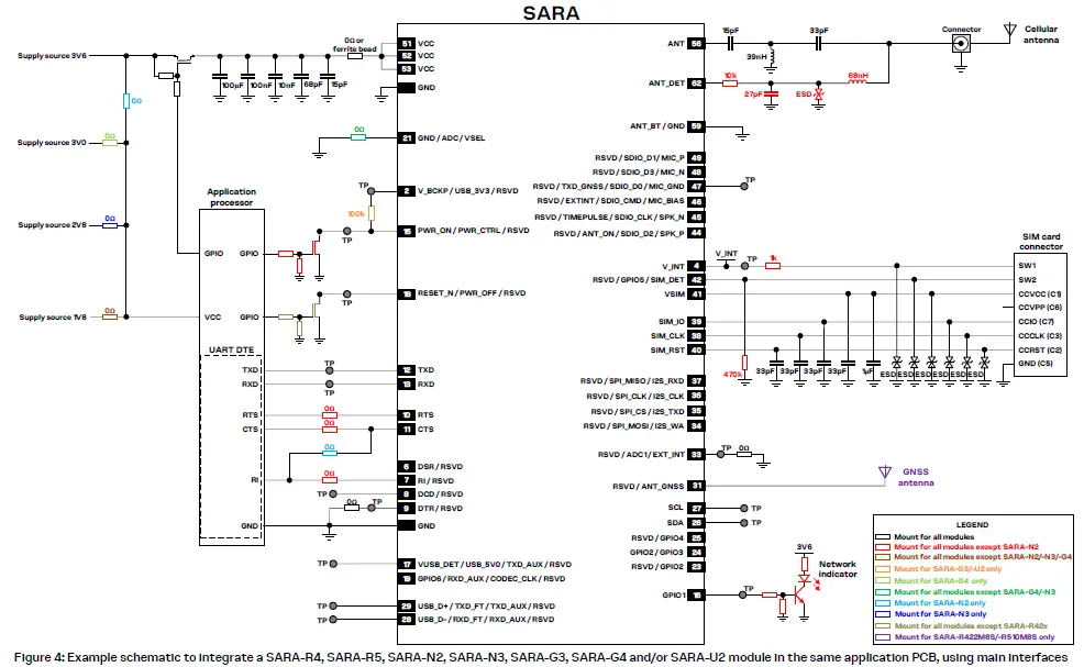
Glossary
Table 8: Explanation of the abbreviations and terms used
| Abbreviation | Definition |
| 2G | 2nd Generation Cellular Technology (GSM, GPRS, EGPRS) |
| 3G | 3rd Generation Cellular Technology (UMTS, HSDPA, HSUPA) |
| 3GPP | 3rd Generation Partnership Project |
| 8-PSK | 8 Phase-Shift Keying modulation |
| ADC | Analog to Digital Converter |
| AT | AT Command Interpreter Software Subsystem, or attention |
| AUX | Auxiliary |
| Cat | Category |
| CDMA | Code Division Multiple Access |
| COAP | Constrained Application Protocol |
| CTS | Clear To Send |
| DCD | Data Carrier Detect |
| DCE | Data Communication Equipment |
| DCS | Digital Cellular System |
| DDC | Display Data Channel interface |
| DL | Down-Link (Reception) |
| DSR | Data Set Ready |
| DTE | Data Terminal Equipment |
| DTLS | Datagram Transport Layer Security |
| DTR | Data Terminal Ready |
| EDGE | Enhanced Data rates for GSM Evolution (EGPRS) |
| EGPRS | Enhanced General Packet Radio Service (EDGE) |
| EMI | Electro-Magnetic Interference |
| ESD | Electro-Static Discharge |
| E-UTRA | Evolved Universal Terrestrial Radio Access |
| FDD | Frequency Division Duplex |
| FOAT | Firmware update Over AT commands |
| FOTA | Firmware update Over The Air |
| FTPS | File Transfer Protocol Secure |
| FW | Firmware |
| GLONASS | Global Navigation Satellite System |
| GMSK | Gaussian Minimum-Shift Keying modulation |
| GND | Ground |
| GNSS | Global Navigation Satellite System |
| GPIO | General Purpose Input Output |
| GPRS | General Packet Radio Service |
| GPS | Global Positioning System |
| GSM | Global System for Mobile communication |
| HSPA | High-Speed Packet Access |
| HTTPS | Hypertext Transfer Protocol Secure |
| I/O | Input/Output |
| Abbreviation | Definition |
| I2C | Inter-Integrated Circuit interface |
| I2S | Inter IC Sound interface |
| IoT | Internet of Things |
| LED | Light Emitting Diode |
| LGA | Land Grid Array |
| LNA | Low Noise Amplifier |
| LPWA | Low Power Wide Area |
| LTE | Long Term Evolution |
| LwM2M | Open Mobile Alliance Lightweight Machine-to-Machine protocol |
| MISO | Master Input Slave Output |
| MOSI | Master Output Slave Input |
| MQTT | Message Queuing Telemetry Transport |
| MQTT-SN | Message Queuing Telemetry Transport for Sensor Networks |
| NB | Narrow Band |
| PCS | Personal Communications Service |
| PMU | Power Management Unit |
| PSM | Power Saving Mode |
| QZSS | Quasi-Zenith Satellite System |
| RAT | Radio Access Technology |
| RF | Radio Frequency |
| RI | Ring Indication |
| RTC | Real Time Clock |
| RTS | Request To Send |
| SAIF | Sub-meter-class Augmentation with Integrity Function |
| SAW | Surface Acoustic Wave |
| SBAS | Satellite-Based Augmentation System |
| SDIO | Secure Digital Input Output |
| SIM | Subscriber Identification Module |
| SMS | Short Message Service |
| SPI | Serial Peripheral Interface |
| TBD | To Be Defined |
| TCP | Transmission Control Protocol |
| TLS | Transport Layer Security |
| TP | Test-Point |
| UART | Universal Asynchronous Receiver-Transmitter |
| UDP | User Datagram Protocol |
| UL | Up-Link (Transmission) |
| UMTS | Universal Mobile Telecommunications System |
| URC | Unsolicited Result Code |
| USB | Universal Serial Bus |
- u-blox SARA-R5 series data sheet, UBX-19016638
- u-blox SARA-R5 series system integration manual, UBX-19041356
- u-blox SARA-R5 series AT commands manual, UBX-19047455
- u-blox SARA-R4 series AT commands manual, UBX-17003787
- u-blox SARA-G3 series data sheet, UBX-13000993
- u-blox SARA-U2 series data sheet, UBX-13005287
- u-blox SARA-N2 series data sheet, UBX-15025564
- u-blox SARA-G3/SARA-U2 series system integration manual, UBX-13000995
- u-blox SARA-N2/SARA-N3 series system integration manual, UBX-17005143
- u-blox nested design application note, UBX-16007243
- u-blox SARA-R4 series data sheet, UBX-16024152
- u-blox SARA-N3 series data sheet, UBX-18066692
- u-blox SARA-G4 series data sheet, UBX-18006165
- u-blox SARA-R4 series system integration manual, UBX-16029218
- u-blox SARA-G4 series system integration manual, UBX-18046432
- u-blox AT commands manual, UBX-13002752
- u-blox SARA-N2/SARA-N3 series AT commands manual, UBX-16014887
For regular updates to u-blox documentation and to receive product change notifications, register on our homepage (www.u-blox.com).
Revision history
| Revision | Date | Name | Comments |
| R01 | 10-Oct-2019 | fvid | Initial release |
| R02 | 11-Nov-2019 | lpah | Updated document products applicability Minor update on SARA-R5 series products description |
| R03 | 24-Jan-2020 | sses | Added SARA-R422, SARA-R422S, SARA-R422M8S products applicability Minor update on SARA-R5 series products description |
| R04 | 09-Mar-2020 | sses | Added SARA-R410M-83B and SARA-R500S products applicability Added jamming detection feature to SARA-R422S and SARA-R422M8S Updated RAT supported by “00” products version of SARA-R5 series modules Minor other corrections and clarifications |
| R05 | 22-Jul-2020 | sses | Updated SARA-R410M-x3B and SARA-R5 series products status Added second auxiliary UART interface on SARA-R42 series modules Added GNSS UART data output on SARA-R422M8S modules Corrected and clarified SARA-R4 series modules operating bands and RATs Revised schematic design example Minor other corrections and clarifications |
| R06 | 12-Oct-2020 | sses | Updated SARA-R5 series and SARA-R42 series products status Revised recommended GNSS diagnostic interface for SARA-R5 series Revised supported bands for SARA-R42 series Minor other corrections and clarifications |
| R07 | 06-Jul-2021 | sses | Extended document applicability to SARA-R410M-02B-03, SARA-R410M-63B-01, SARA-R410M-73B-01, SARA-R410M-83B-01, SARA-R412M-02B-03, SARA-R500S-00B-01, SARA-R500S-01B-00, SARA-R510S-00B-01, SARA-R510S-01B-00, SARA-R510M8S-00B-01 and SARA-R510M8S-01B-00 Updated SARA-R42 series products status Minor other corrections and clarifications |
| R08 | 02-Feb-2022 | fvid | Extended document applicability to SARA-R500S-61B-00, SARA-R500S-71B-00, SARA-R510S-61B-00, SARA-R510S-71B-00, SARA-R510M8S-61B-00, and SARA-R510M8S-71B-00. Updated some product statuses. Minor clarifications. |
Contact
For complete contact information, visit us at www.u-blox.com.
u-blox Offices
North, Central and South America
u-blox America, Inc.
Phone: +1 703 483 3180
[email protected]
Regional Office West Coast:
Phone: +1 408 573 3640
[email protected]
Technical Support:
Phone: +1 703 483 3185
[email protected]
Headquarters
Europe, Middle East, Africa
u-blox AG
Phone: +41 44 722 74 44
Email: [email protected]
Support: [email protected]
Asia, Australia, Pacific
u-blox Singapore Pte. Ltd.
Phone: +65 6734 3811
Email: [email protected]
Support: [email protected]
Regional Office Australia:
Phone: +61 3 9566 7255
Email: [email protected]
Support: [email protected]
Regional Office China (Beijing):
Phone: +86 10 68 133 545
Email: [email protected]
Support: [email protected]
Regional Office China (Chongqing):
Phone: +86 23 6815 1588
Email: [email protected]
Support: [email protected]
Regional Office China (Shanghai):
Phone: +86 21 6090 4832
Email: [email protected]
Support: [email protected]
Regional Office China (Shenzhen):
Phone: +86 755 8627 1083
Email: [email protected]
Support: [email protected]
Regional Office India:
Phone: +91 80 405 092 00
Email: [email protected]
Support: [email protected]
Regional Office Japan (Osaka):
Phone: +81 6 6941 3660
Email: [email protected]
Support: [email protected]
Regional Office Japan (Tokyo):
Phone: +81 3 5775 3850
Email: [email protected]
Support: [email protected]
Regional Office Korea:
Phone: +82 2 542 0861
Email: [email protected]
Support: [email protected]
Regional Office Taiwan:
Phone: +886 2 2657 1090
Email: [email protected]
Support: [email protected]
References
 Roblox
 Home | u-blox
-
Home | u-blox
-
u-blox.com/docs/UBX-13000993
-
u-blox.com/docs/UBX-13000995
-
u-blox.com/docs/UBX-13002752
-
u-blox.com/docs/UBX-13005287
-
u-blox.com/docs/UBX-15025564
-
u-blox.com/docs/UBX-16007243
-
u-blox.com/docs/UBX-16014887
-
u-blox.com/docs/UBX-16024152
-
u-blox.com/docs/UBX-16029218
-
u-blox.com/docs/UBX-17003787
-
u-blox.com/docs/UBX-17005143
-
u-blox.com/docs/UBX-18006165
-
u-blox.com/docs/UBX-18046432
-
u-blox.com/docs/UBX-18066692
-
u-blox.com/docs/UBX-19016638
-
u-blox.com/docs/UBX-19041356
-
u-blox.com/docs/UBX-19047455


