![]() Polarize® and PolarFire SoC DRI
Polarize® and PolarFire SoC DRI
User Guide
Introduction
Microchip’s PolarFire FPGAs are the fifth-generation family of non-volatile FPGA devices, built on state-of-the-art 28 nm non-volatile process technology. PolarFire FPGAs deliver the lowest power at mid-range densities. PolarFire FPGAs lower the cost of mid-range FPGAs by integrating the industry’s lowest power FPGA fabric, lowest power 12.7 Gbps transceiver lane, built-in low power dual PCI Express Gen2 (EP/RP), and, on select data security (S) devices, an integrated low-power crypto co-processor.
Microchip’s PolarFire SoC FPGAs are the fifth-generation family of non-volatile SoC FPGA devices, built on state of-the-art 28 nm non-volatile process technology. The PolarFire SoC family offers industry’s first RISC-V based SoC FPGAs capable of running Linux. The PolarFire SoC family combines a powerful 64-bit 5x core RISC-V Microprocessor Sub-System (MSS), based on SiTime’s U54-MC family, with the PolarFire FPGA fabric in a single device.
Dynamic Reconfiguration Interface (DRI) is an embedded bus within PolarFire and PolarFire SoC FPGAs. DRI is an APB target interconnect providing global access to the following embedded blocks:
- Transceiver lanes
- Transmit PLLs
- PLLs/DLLs (Clock conditioning circuitry or CCCs)
DRI allows modification of these embedded blocks at power-up and during operation. The embedded DRI bus provides dedicated connectivity and register mapped addressing to all the features as APB target peripherals. The DRI connectivity is a fixed dedicated resource that does not require any fabric logic or routing resources. Each transceiver and CCC supports a DRI, which can be enabled to configure its parameters without reprogramming the device. The transceiver, PCIESS, and CCC reconfiguration is controlled by volatile configuration registers that are loaded with values from the flash configuration bits at power-up. It is recommended to carefully use DRI because changing the factory or initialization settings can cause undesired results.
Note: DRI is not available to the user logic, when SmartDebug is being used for debugging.
The following table summarizes DRI access in both PolarFire and PolarFire SoC FPGAs.
Table 1.PolarFire and PolarFire SoC DRI
| DRI Access | PolarFire | PolarFire SoC | Description |
| PF_DRI SgCore IP | ✓ | ✓ | The PF_DRI IP enables user access to the embedded APB target bus which provides a mirrored initiator APB target interface to the FPGA fabric. This IP can be used in both PolarFire and PolarFire SoC FPGAs. In PolarFire designs, the APB initiator can be implemented with the Mi-V soft processor IP or the CoreABC IP for controlling and accessing the DRI target peripherals. In PolarFire SoC designs, the APB initiator can be implemented with the PolarFire SoC MSS, the Mi-V soft processor IP, or the Core ABC IP for controlling and accessing the DRI target peripherals. |
This user guide describes how DRI is used in PolarFire and PolarFire SoC FPGAs.
Note: AXI and APB protocol standards use the terminology “Manager” and “Subordinate”. The equivalent Microchip terminology used in this document is “Initiator” and “Target” respectively.
References
• For detailed information about the PolarFire register map, see PolarFire Device Register Map.
• For detailed information about the PolarFire SoC register map, see PolarFire SoC Device Register Map.
• For more information about PolarFire SoC MSS, see PolarFire SoC FPGA MSS Technical Reference Manual.
• For more information about configuring PolarFire SoC MSS, see PolarFire SoC Standalone MSS Configurator
User Guide available at www.microsemi.com/product-directory/soc-design-tools/5587-pfsoc-mss-configuratortool#documents.
PolarFire FPGA DRI Use Model
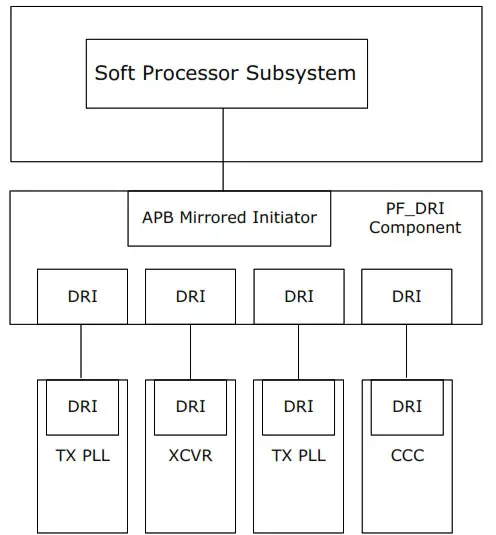
The following figure shows the high-level block diagram of the DRI implementation in PolarFire devices.
Figure 1-1. High-level Block Diagram of DRI Implementation
For information about the dynamic reconfiguration of transceiver and CCC using the PF_DRI IP, see AC475: PolarFire FPGA Dynamic Reconfiguration Interface Application Note.
PolarFire SoC FPGA DRI Block Diagram
In PolarFire SoC FPGAs, MSS accesses DRI via FIC_3 which is an APB interface. The following block diagram shows how DRI is accessed using the PF_DRI IP from the fabric in PolarFire SoC FPGAs.
Figure 2-1. DRI Accessed Using PF_DRI IP from Fabric
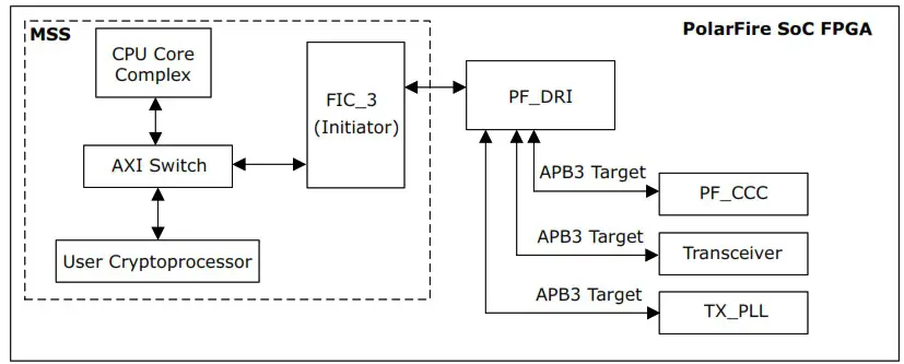
One of the processor cores is used to update the DRI registers of transceiver, CCC, and the TX PLL blocks via the FIC3 interface. For more information about configuring PolarFire SoC MSS, see PolarFire SoC Standalone MSS Configurator User Guide.
For detailed information about the PolarFire SoC register map, see PolarFire SoC Device Register Map.
For more information about updating the CCC PLL outputs dynamically using the PF_DRI IP, see PolarFire SoC Bare Metal DRI Application.
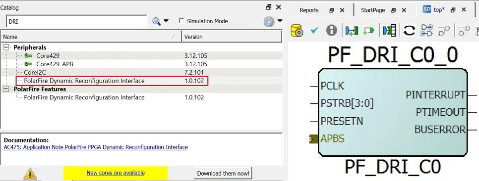
PF_DRI Score IP
PolarFire Dynamic Reconfiguration Interface (PF_DRI) Score IP is available in the Catalog under Peripherals as shown in the following figure.
Figure 3-1. The DRI IP with APB Interface
The following table lists the general ports of the PF_DRI Score.
Table 3-1. PF_DRI Ports
| Port Name | Direction | Width | Description |
| PCLK | Input | 1 | Input clock source to DRI. This clock can be sourced from a CCC or an external oscillator. All transfers on the APB bus are clocked with respect to the rising edge of PCLK. |
| PSTRB[3:0] | Input | 4 | (Active-High) There is one write strobe for each byte of the write data (PWDATA 32-bit or 4 bytes). PSTRB signal indicates the byte lanes to be updated during a write transfer. |
| PRESETN | Input | 1 | (Active-Low) The APB Reset signal from the initiator. |
| PINTERRUPT | Output | 1 | (Active-High) Interrupt can be handled by a soft processor or can be handled by other user logic in the fabric. DRI_INTERRUPT is the source of the INTERRUPT. |
| PTIMEOUT | Output | 1 | (Active-High) Indicates to the fabric that the bus timed out (no response received). Time-out can occur when accessing a target that is not ready. |
| BUSERROR | Output | 1 | (Active-High) Indicates to the fabric that a bus error was detected. Once asserted, this error signal stays active until PRESETN is asserted. Bus error can occur if accessing locked or non-existent targets. |
| APBS (APB Bus Interface bus signals) | — | — | The APBS port is connected to APB initiator. For example, CoreABC/Mi-V Soft Processor. |
| PADDR (input) | 29 | This is the APB address bus driven by the initiator. | |
| PENABLE (input) | 1 | (Active-High) Enable signal from the initiator to trigger APB transfer. | |
| PRDATA (output) | 32 | The selected target drives this data to the initiator during read cycles when PWRITE is Low. | |
| PREADY (output) | 1 | (Active-High) This signal indicates that APB bus is ready for transfer to target. When PREADY is Low, the target initiates a transfer to DRI. | |
| PSEL (input) | 1 | (Active-High) The APB initiator generates this signal to each DRI target. Indicates that the target device is selected and that a data transfer is required. There is a PSELx signal for each target. | |
| PSLVERR (output) | 1 | (Active-High) This signal indicates a transfer failure. | |
| PWDATA (input) | 32 | (Active-High) This bus is driven by the APB initiator during write cycles when PWRITE is High. | |
| PWRITE (input) | 1 | This signal indicates an APB write access when High and an APB read access when Low. |
The following sections describe DRI configuration for XCVR, TX PLL, PCIE, and CCC blocks using the PolarFire Dynamic Reconfiguration Interface Configurator window.
DRI Configuration for XCVR
In the XCVR tab, individual lanes (LANE_0 – 3) can be selected for each quad lane (Qn Lanes, n = 0 – 5) as shown in Figure 3-2. For example, when Q0_LANE0 and Q0_LANE1 lane check boxes are selected in Q0 Lanes, Q0_LANE0 and Q0_LANE1 ports are added to the DRI IP block as shown in Figure 3-2.
Figure 3-2. The XCVR Tab
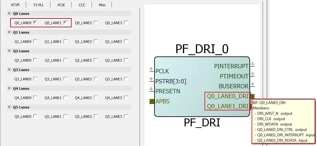
The DRI ports highlighted in the preceding figure are routed through hardwired connections to the transceiver.
The following table describes the DRI ports.
Table 3-2. XCVR DRI Ports
| Port Name | Libero BIF | Direction | Width | Description |
| DRI_ARST_N | — | Output | 1 | Active-Low asynchronous Reset signal from DRI to target. |
| DRI_CLK | — | Output | 1 | Clock source to the target. |
| DRI_WDATA | — | Output | 32 | DRI write data bus driven by DRI during write cycles. |
| Q#_LANE#_DRI_CTRL | Q#_LANE#_DRI | Output | [10:0] | Embedded connection to specified target peripheral. Q# can be 0, 1, 2, 3, 4, 5, LANE# can be 0, 1, 2, 3. |
| Q#_LANE#_DRI_INTERRUPT | Q#_LANE#_DRI | Input | — | Embedded connection to specified target peripheral. Q# can be 0, 1, 2, 3, 4, 5, LANE# can be 0, 1, 2, 3. |
| Q#_LANE#_DRI_RDATA | Q#_LANE#_DRI | Input | [32:0] | Embedded connection to specified target peripheral. Q# can be 0, 1, 2, 3, 4, 5, LANE# can be 0, 1, 2, 3. |
For more information about user connections required while using DRI interface, see AC475: PolarFire FPGA Dynamic Reconfiguration Interface Application Note.
DRI Configuration for TX PLL
In the TX PLL tab, the required options per quad to enable DRI for both spread spectrum generation capable transmit PLLs (Q#_TXPLL_SSC) and (Q#_TXPLLn) without spread spectrum capabilities can be selected as shown in Figure 3-3.
The DRI option is provided for two Q#_TXPLLn (Q#_TXPLL0, Q#_TXPLL1) within transceiver quad locations. For more information, see the “Transmit PLL” section in UG0677: PolarFire FPGA Transceiver User Guide.
Figure 3-3. The TX PLL Tab
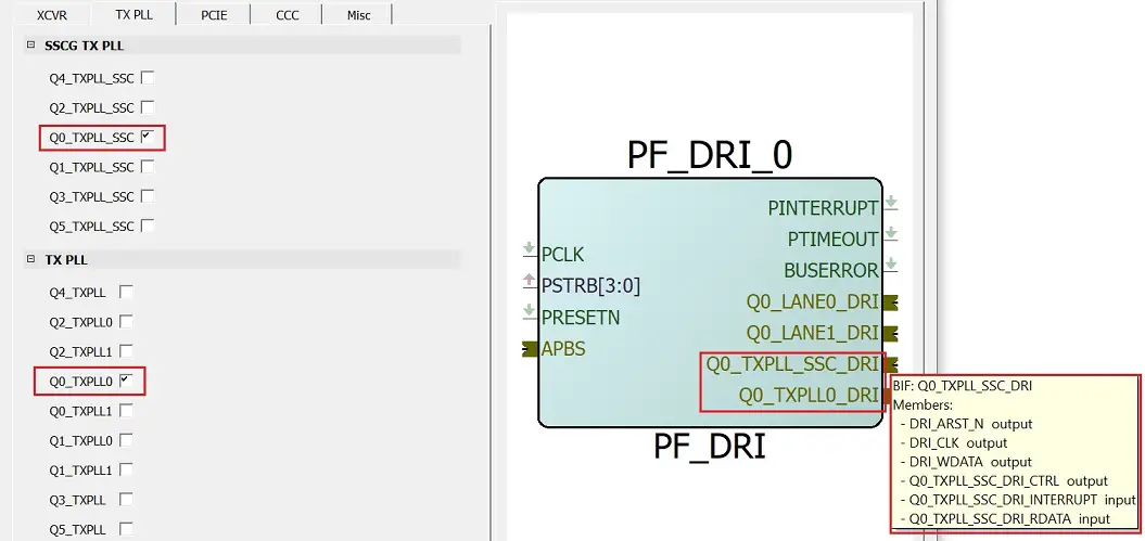
The DRI target ports highlighted in the preceding figure are routed through hardwired connections to the transceiver PLL.
Table 3-3. TX PLL DRI Ports
| Port Name | Libero BIF | Direction | Width | Description |
| Q#_TXPLL_SSC_DRI_CTRL | Q# TXPLL SSC DIRT | Output | [10:0] | Embedded connection to specified target peripheral. Q# can be 0, 1, 2, 3, 4, 5. |
| Q#_TXPLL_SSC_DRI_RDATA | Q#_TXPLL_SSC_ DRI | Input | [32:0] | Embedded connection to specified target peripheral. Q# can be 0, 1, 2, 3, 4, 5. |
| Q#_TXPLL_SSC_DRI_INTERRUPT | Q# TXPLL SSC Input DIRT | Input | Embedded connection to specified target peripheral. Q# can be 0, 1, 2, 3, 4, 5. | |
| Q#_TXPLL_DRI_CTRL | Q#_TXPLL DRI | Output | [10:0] | Embedded connection to specified target peripheral. Q# can be 3, 4, 5. |
| Q#_TXPLL_DRI_RDATA | Q#_TXPLL DRI | Input | [32:0] | Embedded connection to specified target peripheral. Q# can be 3, 4, 5. |
| Q#_TXPLL_DRI_INTERRUPT | Q#_TXPLL DRI | Input | Embedded connection to specified target peripheral. Q# can be 3, 4, 5. | |
| Q#TXPLLO_DRI_CTRL | Q#_TXPLLO DRI | Output | [10:0] | Embedded connection to specified target peripheral. Q# can be 0, 1, 2. |
| Q#_TXPLLO_DRI_RDATA | Q#_TXPLLO DRI | Input | [32:0] | Embedded connection to specified target peripheral. Q# can be 0, 1, 2. |
| Q#_TXPLL0_DRI_INTERRUPT | Q#_TXPLLO DRI | Input | Embedded connection to specified target peripheral. Q# can be 0, 1, 2. | |
| Q#_TXPLL1_DRI_CTRL | Q#_TXPLL1_DRI | Output | [10:0] | Embedded connection to specified target peripheral. Q# can be 0, 1, 2. |
| Q#_TXPLL1_DRI_RDATA | Q#_TXPLL1 DRI | Input | [32:0] | Embedded connection to specified target peripheral. Q# can be 0, 1, 2. |
| Q#_TXPLL1_DRI_INTERRUPT | Q#_TXPLL1_DRI | Input | Embedded connection to specified target peripheral. Q# can be 0, 1, 2. |
DRI Configuration for PCIE
PCIE controllers do not connect directly to a DRI port, the associated XCVR lanes must be connected to the DRI for dynamic control of the XCVR features. The PCIE controllers have a dedicated APB port for access to the register control within the PCIE subsystem. For more information, see UG0685: PolarFire FPGA PCI Express User Guide.
DRI Configuration for CCC
In the CCC tab, the required PLLs and DLLs (in all four corners NW, NE, SE, and SW) can be selected to enable DRI on the selected options and the corresponding DRI target interface is exposed as shown in the following figure.
Figure 3-4. The CCC Tab
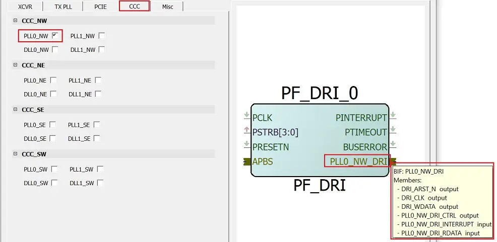
The DRI target ports highlighted in the preceding figure are routed through hardwired connections to the CCC.
The following table lists the CCC DRI ports.
Table 3-4. CCC DRI Ports
| Port Name | Libero BIF | Direction | Width | Description |
| PLL0_**_DRI_CTRL | PLL0_**_DRI | Output | [10:0] | Embedded connection to specified target peripheral. ** can be NW, NE, SW, SE. |
| PLL0_**_DRI_RDATA | PLL0_**_DRI | Input | [32:0] | Embedded connection to specified target peripheral. ** can be NW, NE, SW, SE. |
| PLL0_**_DRI_INTERRUPT | PLL0_**_DRI | Input | — | Embedded connection to specified target peripheral. ** can be NW, NE, SW, SE. |
| PLL1_**_DRI_CTRL | PLL1_**_DRI | Output | [10:0] | Embedded connection to specified target peripheral. ** can be NW, NE, SW, SE. |
| PLL1_**_DRI_RDATA | PLL1_**_DRI | Input | [32:0] | Embedded connection to specified Target peripheral. ** can be NW, NE, SW, SE. |
| PLL1_**_DRI_INTERRUPT | PLL1_**_DRI | Input | — | Embedded connection to specified target peripheral. ** can be NW, NE, SW, SE. |
| DLL0_**_DRI_CTRL | DLL0_**_DRI | Output | [10:0] | Embedded connection to specified target peripheral. ** can be NW, NE, SW, SE. |
| DLL0_**_DRI_RDATA | DLL0_**_DRI | Input | [32:0] | Embedded connection to specified target peripheral. ** can be NW, NE, SW, SE. |
| DLL0_**_DRI_INTERRUPT | DLL0_**_DRI | Input | — | Embedded connection to specified target peripheral. ** can be NW, NE, SW, SE. |
| DLL1_**_DRI_CTRL | DLL1_**_DRI | Output | [10:0] | Embedded connection to specified target peripheral. ** can be NW, NE, SW, SE. |
| DLL1_**_DRI_RDATA | DLL1_**_DRI | Input | [32:0] | Embedded connection to specified target peripheral. ** can be NW, NE, SW, SE. |
| DLL1_**_DRI_INTERRUPT | DLL1_**_DRI | Input | — | Embedded connection to specified target peripheral. ** can be NW, NE, SW, SE. |
Dynamic Configuration of CCC
Each CCC has a DRI which can be enabled to configure CCC parameters without reprogramming the device. The CCC configuration is controlled by the volatile configuration registers that are loaded with values from the flash configuration bits at power-up. An APB bus initiator must be interfaced to the CCC using a DRI macro for dynamic configuration. The APB bus initiator is used to dynamically modify the CCC configuration register values as per design needs. For more information on CCC configuration registers and their bit definitions, see PolarFire Device Register Map.
To meet all the datasheet specifications, certain requirements must be met when configuring the PLL/DLL parameters. The Libero CCC configurator implements all these requirements and creates a valid solution for the requested output clock frequencies and phases. Hence, Microchip recommends that users generate the required configuration using Libero CCC configurator and use the generated parameters in their dynamic configuration solution.
The PLL_POWERDOWN_N input must be asserted before making changes to the PLL configuration parameters.
Note: Asserting the PLL_POWERDOWN_N signal resets the PLL operation.
When the CCC is configured in internal Post-VCO feedback mode, if the requirement is to change the phase or output divider configuration then the clock start/stop (OUT#_EN) signals can be used to stop the clock output before making the changes for a glitch free configuration.
The following steps describe how to perform dynamic configuration of CCC:
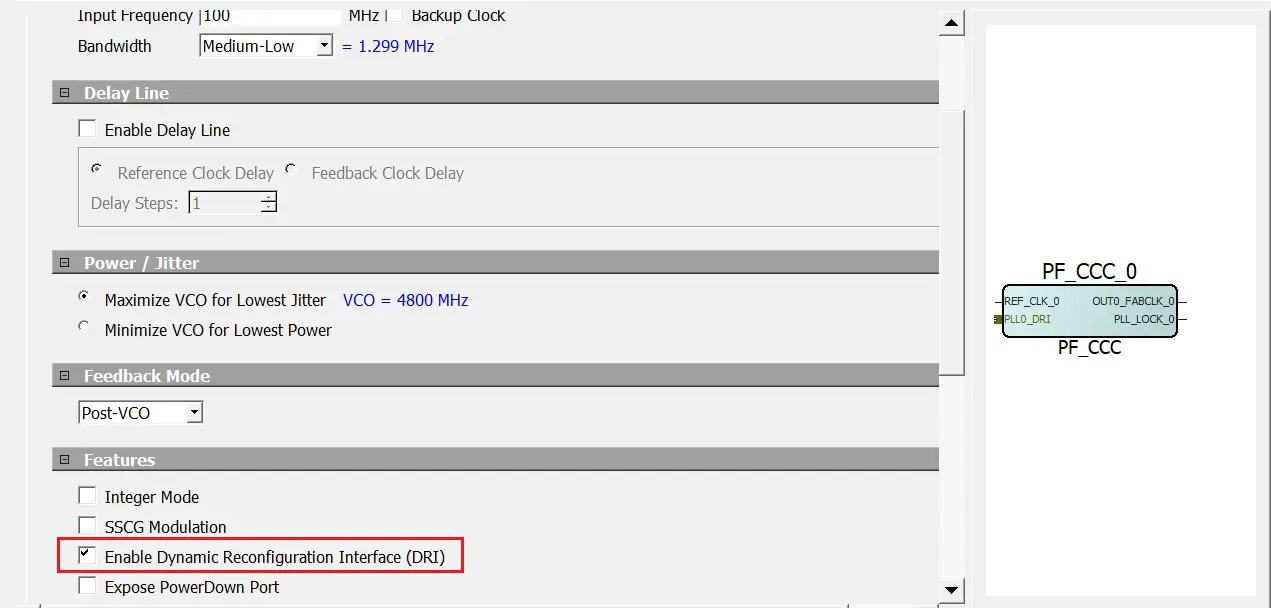
- Select Enable Dynamic Reconfiguration Interface under the Features section of CCC configurator as shown in Figure 3-5.
Figure 3-5. DRI Option in CCC This enables and exposes the DRI on the instantiated CCC component as shown in the above figure.
 - Instantiate and configure a PF_DRI SgCore with the required PLL enabled into the Smartening. The dynamic reconfiguration interface macro converts the APB interface signals to CCC dynamic reconfiguration interface signals. The DRI interface for the selected PLL is exposed on the PF_DRI macro. The APB port of DRI are shown in Figure 3-4. The DRI ports cannot be monitored or altered in the Libero design. These ports are used to facilitate HDL simulation of changes made to the CCC over the DRI. The PF_DRI SgCore converts standard APB3 read/writes to DRI transactions.
- Double click the DRI macro to configure.
- In the PF_DRI configurator, under the CCC tab, select the PLLs and DLLs that need dynamic configuration. The DRI macro interface is shown in Figure 3-4.
- Connect the APB initiator port from an APB initiator (for example, Core ABC) to the mirrored initiator port of PF_DRI as shown in the following figure.
Figure 3-6. CCC Dynamic Configuration System
 This enables and exposes the DRI on the instantiated CCC component as shown in the above figure.
Misc Tab
In the Misc tab, the CRYPTO option can be selected to enable DRI on CRYPTO as shown in Figure 3-7.
Note: The Enable latency simulation option is currently not supported.
Figure 3-7. Enabling DRI on CRYPTO
The following table lists the CRYPTO DRI ports.
Table 3-5. CRYPTO DRI Ports
| Port Name | Libero BIF | Direction | Width | Description |
| CRYPTO_DRI_CTRL | CRYPTO_DRI | Output | [10:0] | Embedded connection to specified target peripheral. |
| CRYPTO_DRI_RDATA | CRYPTO_DRI | Input | [32:0] | Embedded connection to specified target peripheral. |
| CRYPTO_DRI_INTERRUPT | CRYPTO_DRI | Input | — | Embedded connection to specified target peripheral. |
Note: The ports highlighted in the above table are routed through hardwired connections to the User Crypto Processor.
Functional Timing Diagram
Figure 3-8 shows the DRI timing diagram.
Figure 3-8. APB Initiator Timing Diagram
For more information about FPD_PCLK, see DS0141: PolarFire FPGA Datasheet.
The SDC constraint is derived and generated automatically based on the connection of the PF_DRI IP to its APB initiator and to the DRI peripherals. Static Timing Analysis (STA) of PCLK (FPD_PCLK) with SmartPower gives the minimum and maximum analysis of the APB interface Tus/thud parameters.
Revision History
The revision history table describes the changes that were implemented in the document. The changes are listed by revision, starting with the most current publication.
Table 4-1. Revision History
| Revision | Date | Description |
| A | 06/2021 | The first publication of this document. |
The Microchip Website
Microchip provides online support via our website at www.microchip.com/. This website is used to make files and information easily available to customers. Some of the content available includes:
- Product Support – Data sheets and errata, application notes and sample programs, design resources, user’s guides and hardware support documents, latest software releases and archived software
- General Technical Support – Frequently Asked Questions (FAQs), technical support requests, online discussion groups, Microchip design partner program member listing
- Business of Microchip – Product selector and ordering guides, latest Microchip press releases, listing of seminars and events, listings of Microchip sales offices, distributors and factory representatives
Product Change Notification Service
Microchip’s product change notification service helps keep customers current on Microchip products. Subscribers will receive email notification whenever there are changes, updates, revisions or errata related to a specified product family or development tool of interest.
To register, go to www.microchip.com/pcn and follow the registration instructions.
Customer Support
Users of Microchip products can receive assistance through several channels:
- Distributor or Representative
- Local Sales Office
- Embedded Solutions Engineer (ESE)
- Technical Support
Customers should contact their distributor, representative or ESE for support. Local sales offices are also available to help customers. A listing of sales offices and locations is included in this document.
Technical support is available through the website at: www.microchip.com/support
Microchip Devices Code Protection Feature
Note the following details of the code protection feature on Microchip devices:
- Microchip products meet the specifications contained in their particular Microchip Data Sheet.
- Microchip believes that its family of products is secure when used in the intended manner and under normal conditions.
- There are dishonest and possibly illegal methods being used in attempts to breach the code protection features of the Microchip devices. We believe that these methods require using the Microchip products in a manner outside the operating specifications contained in Microchip’s Data Sheets. Attempts to breach these code protection features, most likely, cannot be accomplished without violating Microchip’s intellectual property rights.
- Microchip is willing to work with any customer who is concerned about the integrity of its code.
- Neither Microchip nor any other semiconductor manufacturer can guarantee the security of its code. Code protection does not mean that we are guaranteeing the product is “unbreakable.” Code protection is constantly evolving. We at Microchip are committed to continuously improving the code protection features of our products. Attempts to break Microchip’s code protection feature may be a violation of the Digital Millennium Copyright Act. If such acts allow unauthorized access to your software or other copyrighted work, you may have a right to sue for relief under that Act.
Legal Notice
Information contained in this publication is provided for the sole purpose of designing with and using Microchip products. Information regarding device applications and the like is provided only for your convenience and may be superseded by updates. It is your responsibility to ensure that your application meets with your specifications.
THIS INFORMATION IS PROVIDED BY MICROCHIP “AS IS”. MICROCHIP MAKES NO REPRESENTATIONS OR WARRANTIES OF ANY KIND WHETHER EXPRESS OR IMPLIED, WRITTEN OR ORAL, STATUTORY OR OTHERWISE, RELATED TO THE INFORMATION INCLUDING BUT NOT LIMITED TO ANY IMPLIED WARRANTIES OF NON-INFRINGEMENT, MERCHANTABILITY, AND FITNESS FOR A PARTICULAR PURPOSE OR WARRANTIES RELATED TO ITS CONDITION, QUALITY, OR PERFORMANCE.
IN NO EVENT WILL MICROCHIP BE LIABLE FOR ANY INDIRECT, SPECIAL, PUNITIVE, INCIDENTAL OR CONSEQUENTIAL LOSS, DAMAGE, COST OR EXPENSE OF ANY KIND WHATSOEVER RELATED TO THE INFORMATION OR ITS USE, HOWEVER CAUSED, EVEN IF MICROCHIP HAS BEEN ADVISED OF THE POSSIBILITY OR THE DAMAGES ARE FORESEEABLE. TO THE FULLEST EXTENT ALLOWED BY LAW, MICROCHIP’S TOTAL LIABILITY ON ALL CLAIMS IN ANY WAY RELATED TO THE INFORMATION OR ITS USE WILL NOT EXCEED THE AMOUNT OF FEES, IF ANY, THAT YOU HAVE PAID DIRECTLY TO MICROCHIP FOR THE INFORMATION. Use of Microchip devices in life support and/or safety applications is entirely at the buyer’s risk, and the buyer agrees to defend, indemnify and hold harmless Microchip from any and all damages, claims, suits, or expenses resulting from such use. No licenses are conveyed, implicitly or otherwise, under any Microchip intellectual property rights unless otherwise stated.
Trademarks
The Microchip name and logo, the Microchip logo, Adaptec, AnyRate, AVR, AVR logo, AVR Freaks, BesTime, BitCloud, chipKIT, chipKIT logo, Crypto Memory, Cryptor, dsPIC, FlashFlex, flexPWR, HELDO, IGLOO, JukeBlox, KeeLoq, Kleer, LANCheck, LinkMD, maXStylus, maXTouch, Medially, megaAVR, Microsemi, Microsemi logo, MOST, MOST logo, MPLAB, OptoLyzer, PackeTime, PIC, picoPower, PICSTART, PIC32 logo, PolarFire, Prochip Designer, QTouch, SAM-BA, SenGenuity, SpyNIC, SST, SST Logo, SuperFlash, Symmetricom, SyncServer, Tachyon, TimeSource, tinyAVR, UNI/O, Vectron, and XMEGA are registered trademarks of Microchip Technology Incorporated in the U.S.A. and other countries.
AgileSwitch, APT, ClockWorks, The Embedded Control Solutions Company, EtherSynch, FlashTec, Hyper Speed Control, Hyperlight Load, Intel limos, Libero, motorBench, mTouch, Powermite 3, Precision Edge, ProASIC, ProASIC Plus, ProASIC Plus logo, Quiet-Wire, SmartFusion, SyncWorld, Timex, TimeCesium, TimeHub, TimePictra, TimeProvider, WinPath, and ZL are registered trademarks of Microchip Technology Incorporated in the U.S.A. Adjacent Key Suppression, AKS, Analog-for-the-Digital Age, Any Capacitor, AnyIn, AnyOut, Augmented Switching, BlueSky, BodyCom, CodeGuard, CryptoAuthentication, CryptoAutomotive, CryptoCompanion, CryptoController, dsPICDEM, dsPICDEM.net, Dynamic Average Matching, DAM, ECAN, Espresso T1S, EtherGREEN, IdealBridge, In-Circuit Serial Programming, ICSP, INICnet, Intelligent Paralleling, Inter-Chip Connectivity, JitterBlocker, maxCrypto, maxView, memBrain, Mindi, MiWi, MPASM, MPF, MPLAB Certified logo, MPLIB, MPLINK, MultiTRAK, NetDetach, Omniscient Code Generation, PICDEM, PICDEM.net, PICkit, PICtail, PowerSmart, PureSilicon, QMatrix, REAL ICE, Ripple Blocker, RTAX, RTG4, SAM-ICE, Serial Quad I/O, simpleMAP, SimpliPHY, SmartBuffer, SMART-I.S., storClad, SQI, SuperSwitcher, SuperSwitcher II, Switchtec, SynchroPHY, Total Endurance, TSHARC, USBCheck, VariSense, VectorBlox, VeriPHY, ViewSpan, WiperLock, XpressConnect, and ZENA are trademarks of Microchip Technology Incorporated in the U.S.A. and other countries.
SQTP is a service mark of Microchip Technology Incorporated in the U.S.A.
The Adaptec logo, Frequency on Demand, Silicon Storage Technology, and Symmcom are registered trademarks of Microchip Technology Inc. in other countries.
GestIC is a registered trademark of Microchip Technology Germany II GmbH & Co. KG, a subsidiary of Microchip Technology Inc., in other countries. All other trademarks mentioned herein are property of their respective companies. © 2021, Microchip Technology Incorporated, Printed in the U.S.A., All Rights Reserved. ISBN: 978-1-5224-8315-1
Quality Management System
For information regarding Microchip’s Quality Management Systems, please visit www.microchip.com/quality.
Worldwide Sales and Service
| AMERICAS | ASIA/PACIFIC | ASIA/PACIFIC | EUROPE |
| Corporate Office 2355 West Chandler Blvd. Chandler, AZ 85224-6199 Tel: 480-792-7200 Fax: 480-792-7277 Technical Support: www.microchip.com/support Web Address: www.microchip.com Atlanta Duluth, GA Tel: 678-957-9614 Fax: 678-957-1455 Austin, TX Tel: 512-257-3370 Boston Westborough, MA Tel: 774-760-0087 Fax: 774-760-0088 Chicago Itasca, IL Tel: 630-285-0071 Fax: 630-285-0075 Dallas Addison, TX Tel: 972-818-7423 Fax: 972-818-2924 Detroit Novi, MI Tel: 248-848-4000 Houston, TX Tel: 281-894-5983 Indianapolis Noblesville, IN Tel: 317-773-8323 Fax: 317-773-5453 Tel: 317-536-2380 Los Angeles Mission Viejo, CA Tel: 949-462-9523 Fax: 949-462-9608 Tel: 951-273-7800 Raleigh, NC Tel: 919-844-7510 New York, NY Tel: 631-435-6000 San Jose, CA Tel: 408-735-9110 Tel: 408-436-4270 Canada – Toronto Tel: 905-695-1980 Fax: 905-695-2078 | Australia – Sydney Tel: 61-2-9868-6733 China – Beijing Tel: 86-10-8569-7000 China – Chengdu Tel: 86-28-8665-5511 China – Chongqing Tel: 86-23-8980-9588 China – Dongguan Tel: 86-769-8702-9880 China – Guangzhou Tel: 86-20-8755-8029 China – Hangzhou Tel: 86-571-8792-8115 China – Hong Kong SAR Tel: 852-2943-5100 China – Nanjing Tel: 86-25-8473-2460 China – Qingdao Tel: 86-532-8502-7355 China – Shanghai Tel: 86-21-3326-8000 China – Shenyang Tel: 86-24-2334-2829 China – Shenzhen Tel: 86-755-8864-2200 China – Suzhou Tel: 86-186-6233-1526 China – Wuhan Tel: 86-27-5980-5300 China – Xian Tel: 86-29-8833-7252 China – Xiamen Tel: 86-592-2388138 China – Zhuhai Tel: 86-756-3210040 | India – Bangalore Tel: 91-80-3090-4444 India – New Delhi Tel: 91-11-4160-8631 India – Pune Tel: 91-20-4121-0141 Japan – Osaka Tel: 81-6-6152-7160 Japan – Tokyo Tel: 81-3-6880- 3770 Korea – Daegu Tel: 82-53-744-4301 Korea – Seoul Tel: 82-2-554-7200 Malaysia – Kuala Lumpur Tel: 60-3-7651-7906 Malaysia – Penang Tel: 60-4-227-8870 Philippines – Manila Tel: 63-2-634-9065 Singapore Tel: 65-6334-8870 Taiwan – Hsin Chu Tel: 886-3-577-8366 Taiwan – Kaohsiung Tel: 886-7-213-7830 Taiwan – Taipei Tel: 886-2-2508-8600 Thailand – Bangkok Tel: 66-2-694-1351 Vietnam – Ho Chi Minh Tel: 84-28-5448-2100 | Austria – Wels Tel: 43-7242-2244-39 Fax: 43-7242-2244-393 Denmark – Copenhagen Tel: 45-4485-5910 Fax: 45-4485-2829 Finland – Espoo Tel: 358-9-4520-820 France – Paris Tel: 33-1-69-53-63-20 Fax: 33-1-69-30-90-79 Germany – Garching Tel: 49-8931-9700 Germany – Haan Tel: 49-2129-3766400 Germany – Heilbronn Tel: 49-7131-72400 Germany – Karlsruhe Tel: 49-721-625370 Germany – Munich Tel: 49-89-627-144-0 Fax: 49-89-627-144-44 Germany – Rosenheim Tel: 49-8031-354-560 Israel – Ra’anana Tel: 972-9-744-7705 Italy – Milan Tel: 39-0331-742611 Fax: 39-0331-466781 Italy – Padova Tel: 39-049-7625286 Netherlands – Drunen Tel: 31-416-690399 Fax: 31-416-690340 Norway – Trondheim Tel: 47-72884388 Poland – Warsaw Tel: 48-22-3325737 Romania – Bucharest Tel: 40-21-407-87-50 Spain – Madrid Tel: 34-91-708-08-90 Fax: 34-91-708-08-91 Sweden – Gothenberg Tel: 46-31-704-60-40 Sweden – Stockholm Tel: 46-8-5090-4654 UK – Wokingham Tel: 44-118-921-5800 Fax: 44-118-921-5820 |
© 2021 Microchip Technology Inc.
DS60001711A-page 19


