![]() Azurite 9×9 Evaluation Board
Azurite 9×9 Evaluation Board
Hardware User’s Guide
Azurite 9×9 Evaluation Board Hardware
Note the following details of the code protection feature on Microchip products:
- Microchip products meet the specifications contained in their particular Microchip Data Sheet.
- Microchip believes that its family of products is secure when used in the intended manner, within operating specifications, and under normal conditions.
- Microchip values and aggressively protects its intellectual property rights. Attempts to breach the code protection features of Microchip product is strictly prohibited and may violate the Digital Millennium Copyright Act.
- Neither Microchip nor any other semiconductor manufacturer can guarantee the security of its code. Code protection does not mean that we are guaranteeing the product is “unbreakable”. Code protection is constantly evolving. Microchip is committed to continuously improving the code protection features of our products.
This publication and the information herein may be used only with Microchip products, including to design, test, and integrate Microchip products with your application. Use of this information in any other manner violates these terms. Information regarding device applications is provided only for your convenience and may be superseded by updates. It is your responsibility to ensure that your application meets with your specifications. Contact your local Microchip sales office for additional support or, obtain additional support at https://www.microchip.com/en-us/support/design-help/client-supportservices.
THIS INFORMATION IS PROVIDED BY MICROCHIP “AS IS”. MICROCHIP MAKES NO REPRESENTATIONS OR WARRANTIES OF ANY KIND WHETHER EXPRESS OR IMPLIED, WRITTEN OR ORAL, STATUTORY OR OTHERWISE, RELATED TO THE INFORMATION INCLUDING BUT NOT LIMITED TO ANY IMPLIED WARRANTIES OF NONINFRINGEMENT, MERCHANTABILITY, AND FITNESS FOR A PARTICULAR PURPOSE, OR WARRANTIES RELATED TO ITS CONDITION, QUALITY, OR PERFORMANCE.
IN NO EVENT WILL MICROCHIP BE LIABLE FOR ANY INDIRECT, SPECIAL, PUNITIVE, INCIDENTAL, OR CONSEQUENTIAL LOSS, DAMAGE, COST, OR EXPENSE OF ANY KIND WHATSOEVER RELATED TO THE INFORMATION OR ITS USE, HOWEVER CAUSED, EVEN IF MICROCHIP HAS BEEN ADVISED OF THE POSSIBILITY OR THE DAMAGES ARE FORESEEABLE. TO THE FULLEST EXTENT ALLOWED BY LAW, MICROCHIP’S TOTAL LIABILITY ON ALL CLAIMS IN ANY WAY RELATED TO THE INFORMATION OR ITS USE WILL NOT EXCEED THE AMOUNT OF FEES, IF ANY, THAT YOU HAVE PAID DIRECTLY TO MICROCHIP FOR THE INFORMATION.
Use of Microchip devices in life support and/or safety applications is entirely at the buyer’s risk, and the buyer agrees to defend, indemnify and hold harmless Microchip from any and all damages, claims, suits, or expenses resulting from such use. No licenses are conveyed, implicitly or otherwise, under any Microchip intellectual property rights unless otherwise stated.
Trademarks
The Microchip name and logo, the Microchip logo, Adaptec, AnyRate, AVR, AVR logo, AVR Freaks, BesTime, BitCloud, CryptoMemory, CryptoRF, dsPIC, flexPWR, HELDO, IGLOO, JukeBlox, KeeLoq, Kleer, LANCheck, LinkMD, maXStylus, maXTouch, MediaLB, megaAVR, Microsemi, Microsemi logo, MOST, MOST logo, MPLAB, OptoLyzer, PIC, picoPower, PICSTART, PIC32 logo, PolarFire, Prochip Designer, QTouch, SAM-BA, SenGenuity, SpyNIC, SST, SST Logo, SuperFlash, Symmetricom, SyncServer, Tachyon, TimeSource, tinyAVR, UNI/O, Vectron, and XMEGA are registered trademarks of Microchip Technology Incorporated in the U.S.A. and other countries.
AgileSwitch, APT, ClockWorks, The Embedded Control Solutions Company, EtherSynch, Flashtec, Hyper Speed Control, HyperLight Load, IntelliMOS, Libero, motorBench, mTouch, Powermite 3, Precision Edge, ProASIC, ProASIC Plus, ProASIC Plus logo, Quiet- Wire, SmartFusion, SyncWorld, Temux, TimeCesium, TimeHub,
TimePictra, TimeProvider, TrueTime, WinPath, and ZL are registered trademarks of Microchip Technology Incorporated in the U.S.A.
Adjacent Key Suppression, AKS, Analog-for-the-Digital Age, Any Capacitor, AnyIn, AnyOut, Augmented Switching, BlueSky, BodyCom, CodeGuard, CryptoAuthentication, CryptoAutomotive, CryptoCompanion, CryptoController, dsPICDEM, dsPICDEM.net, Dynamic Average Matching, DAM, ECAN, Espresso T1S, EtherGREEN, GridTime, IdealBridge, In-Circuit Serial Programming, ICSP, INICnet, Intelligent Paralleling, Inter-Chip Connectivity, JitterBlocker, Knob-on-Display, maxCrypto, maxView,
memBrain, Mindi, MiWi, MPASM, MPF, MPLAB Certified logo, MPLIB, MPLINK, MultiTRAK, NetDetach, NVM Express, NVMe, Omniscient Code Generation, PICDEM, PICDEM.net, PICkit, PICtail, PowerSmart, PureSilicon, QMatrix, REAL ICE, Ripple Blocker, RTAX, RTG4, SAM-ICE, Serial Quad I/O, simpleMAP, SimpliPHY, SmartBuffer, SmartHLS, SMART-I.S., storClad, SQI, SuperSwitcher, SuperSwitcher II, Switchtec, SynchroPHY, Total Endurance, TSHARC, USBCheck, VariSense, VectorBlox, VeriPHY, ViewSpan, WiperLock, XpressConnect, and ZENA are trademarks of Microchip Technology Incorporated in the U.S.A. and other countries.
SQTP is a service mark of Microchip Technology Incorporated in
the U.S.A.
The Adaptec logo, Frequency on Demand, Silicon Storage Technology, Symmcom, and Trusted Time are registered
trademarks of Microchip Technology Inc. in other countries. GestIC is a registered trademark of Microchip Technology Germany II GmbH & Co. KG, a subsidiary of Microchip Technology Inc., in other countries.
All other trademarks mentioned herein are property of their respective companies.
© 2022, Microchip Technology Incorporated and its subsidiaries.
All Rights Reserved.
ISBN: 978-1-5224-9900-8
For information regarding Microchip’s Quality Management Systems,
please visit www.microchip.com/quality.
NOTES:
Chapter 1. Hardware Overview
1.1 SUPPORTED DEVICES
The Azurite 9×9 Evaluation Board supports Azurite-family devices packaged in the 9 mm x 9 mm VQFN package.
1.2 RELATED DOCUMENTS
- Azurite 9 mm x 9 mm Evaluation Board Schematic
- Azurite 9 mm x 9 mm Evaluation Board Bill of Materials
- Data sheets for the part numbers listed in the Supported Devices section.
1.3 HARDWARE FEATURE SUMMARY
Azurite 9×9 Evaluation Board is a test and demonstration platform with support for the full feature sets of the Azurite family of timing ICs.
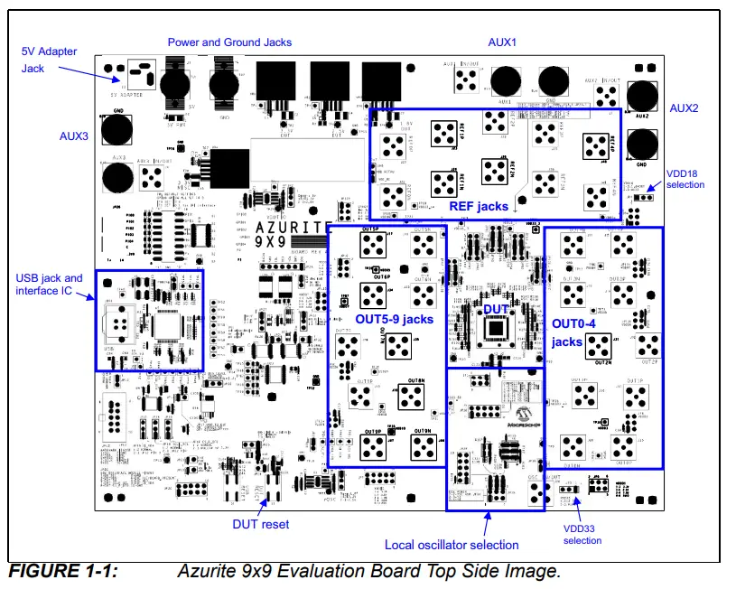
A top side image of the board is shown in Figure 1-1. Throughout this document, the abbreviation “DUT” is used to refer to “Device Under Test”, meaning the Microchip timing IC on the board.
The board includes the following major components and hardware features:
1.3.1 Major Components
- Timing IC (DUT)
- Low noise linear regulators
- USB Interface for optional connection to PC with GUI software
- SMA connectors for access to all DUT clocks
1.3.2 Hardware Features
- Single 5VDC external power interface with connector for AC/DC wall adapter
- Fully configurable DUT power options
- DUT reset switch
- USB interface with USB-B connector for PC GUI connection
- Pin headers with direct access to board’s SPI/I2C bus. Board can provide interface for GUI to control off-boardDUT, or external SPI master device can interface with on-board DUT.
- Status LEDs
- Oscillator options: on-board crystal, on board XO, XO on daughter card, or separate oscillator board
- SMA connectors on all input and output clocks
- Jumper-configurable termination and coupling
- Additional discrete component configuration options for advanced users
1.3.3 Power Supply
The board is normally powered via connector J3 using the provided AC wall-plug 5VDC power supply. Red LED D2 illuminates to indicate that the board is powered. Advanced power options for lab experimentation are also provisioned on the board.
1.3.4 USB Interface
The Windows® -based Microchip Timing GUI software communicates with the board via USB connector JDR1.
Chapter 2. Hardware Configuration
To provide flexibility to users, the board supports several configurations, some of which require GUI supervision via USB. Other configurations provide external device access points to the board’s serial bus by means of pin headers.
2.1 DUT SERIAL INTERFACE
The board supports operating the DUT serial interface in either SPI or I2C mode. The bus master can be either the on-board USB Device U5 or an external bus master connected to JP12 or JP20. Modes 1 through 4 in Table 2-1 define how to configure the board for each bus master/bus mode combination. Table 2-2 defines the pinout for connector JP20. Table 2-3 defines the pinout for connector JP12. For both connectors, pins 4 and 6 should be left unconnected.
TABLE 2-1: EVALUATION BOARD SERIAL BUS MODES
| Mode | Serial Bus Master | Serial Bus Slave | Description | Switch and Jumper Settings | Notes |
| 1 | On-board USB device (SPI) | On-board DUT (SPI) | The GUI/PC uses the on-board USB device as a SPI master to communicate with the on-board DUT configured as a SPI slave. | JP17 = no shunt JP14 = Shunt pins 1-2 JP15 = Shunt pins 1-2 JP16 = Shunt pins 1-2 SW1[6] CS_B_IF0 = 1 (SPI interface) SW1[7] SO_IF1 = 0 or 1 | Default |
| 2 | On-board USB device (I2C) | On-board DUT (I2C) | The GUI/PC uses the on-board USB device as an I2C master to communicate with the on-board DUT configured as an I2C slave. | JP17 = no shunt JP14 = Shunt pins 1-2 JP15 = Shunt pins 1-2 JP16 = Shunt pins 1-2 SW1[6] CS_B_IF0 = 0 (I2C interface) SW1[7] SO_IF1: 0 = default I2C slave address 0111000 1 = default I2C slave address 0111001 | — |
| 3 | Off-board Bus master on JP12 or JP20 (SPI) | On-board DUT (SPI) | An off-board SPI master connected to either JP12 or JP20 communicates with the on-board DUT configured as a SPI slave. | JP17 = Shunt pins 1-2 JP14 = Shunt pins 1-2 JP15 = Shunt pins 1-2 JP16 = Shunt pins 1-2 If master is ZLE302USB USB Inter- face Module connected to JP12: JP13 = Shunt pins 1-2 If master is Aardvark connected to JP12: JP13 = no shunt SW1[6] CS_B_IF0 = 1 (SPI interface) SW1[7] SO_IF1 = 0 or 1 | — |
TABLE 2-1: EVALUATION BOARD SERIAL BUS MODES (CONTINUED)
| Mode | Serial Bus Master | Serial Bus Slave | Description | Switch and Jumper Settings | Notes |
| 4 | Off-board Bus master on JP12 or JP20 (I2C) | On-board DUT (I2C) | An off-board I2C master connect to either JP12 or JP20 communicates with the on-board DUT configured as an I2C slave. | JP17 = Shunt pins 1-2 JP14 = Shunt pins 1-2 JP15 = Shunt pins 1-2 JP16 = Shunt pins 1-2 If master is ZLE302USB USB Inter- face Module connected to JP12: JP13 = Shunt pins 1-2 If master is Aardvark connected to JP12: JP13 = no shunt SW1[6] CS_B_IF0 = 0 (I2C interface) SW1[7] SO_IF1: 0 = default I2C slave address 0111000 1 = default I2C slave address 0111001 | Note 1 |
| 5 | On-board USB device (SPI) | Off-board DUT connect to JP12 or JP20 (SPI) | The GUI/PC uses the on-board USB device as a SPI master to communicate with an off-board DUT config- ured as a SPI slave and connected to JP12 or JP20. | JP17 = no shunt JP14 = Shunt pins 1-2 JP15 = Shunt pins 1-2 JP16 = Shunt pins 2-3 SW1[6] CS_B_IF0 = 1 (SPI interface) SW1[7] SO_IF1 = 0 or 1 | — |
| 6 | On-board USB device (I2C) | Off-board DUT connect to JP12 or JP20 (I2C) | The GUI/PC uses the on-board USB device as an I2C master to communicate with an off-board DUT config- ured as a I2C slave and connected to JP12 or JP20. | JP17 = no shunt JP14: Shunt pins 2-3 JP15: Shunt pins 2-3 JP16: Shunt pins 1-2 SW1[6] CS_B_IF0 = 0 (I2C interface) SW1[7] SO_IF1: 0 = default I2C slave address 0111000 1 = default I2C slave address 0111001 | — |
Note 1: Set JP14 = 2-3 and JP15 = 2-3 to support Total Phase Aardvark Adapter I2C mode pinout.
TABLE 2-2: CONNECTOR JP20 PINOUT
| Pin | Signal | Description |
| 1 | BR_SCL | Board Resource I2C Serial Clock |
| 2 | GND | Ground |
| 3 | BR_SDA | Board Resource I2C Serial Data |
| 4 | DUT_RST_B/BOARD_PRESENT | Do not connect |
| 5 | DUT_SO | DUT SPI Master In Slave Out |
| 6 | DUT_VDD | Do not connect |
| 7 | DUT_SCK_SCL | DUT SPI Clock/I2C Clock |
| 8 | DUT_SI_SDA | DUT SPI Master Out Slave In/I2C Data |
| 9 | DUT_CS_B | DUT Chip Select |
| 10 | GND | Ground |
TABLE 2-3: CONNECTOR JP12 PINOUT
| Pin | Signal | Description |
| 1 | SCL | I2C Serial Clock |
| 2 | GND | Ground |
| 3 | SDA | I2C Serial Data |
| 4 | NC | Do not connect |
| 5 | MISO | SPI Master In Slave Out |
| 6 | NC | Do not connect |
| 7 | SCLK | SPI Clock |
| 8 | MOSI | SPI Master Out Slave In |
| 9 | SS | Slave Select |
| 10 | GND | Ground |
2.2 DUT RESET SWITCH
DUT reset can be initiated in one of two ways:
- Press momentary switch S2
- Software: Set U1 bit port ADBUS5 as output pin and toggle it low, then high.
Additionally, the evaluation board supports the hardware-configurable DUT reset options listed in Table 2-4.
TABLE 2-4: DUT RESET HARDWARE CONFIGURATION
| Silkscreen Reference | Device/ Function | Basic Setting | Schematic Sheet | Description |
| JP18 | 2-pin header | Shunt Installed | 4 | USB device DUT reset control enable Uninstalled = Disabled Installed = Enabled |
| JP24 | 2-pin header | Shunt Installed | 4 | S2 and POR device, DUT reset control enable Uninstalled = Disabled Installed = Enabled |
| JP21 | 2-pin header | Shunt Installed | 4 | External SPI/I2C master pin JP14.4 reset control enable Uninstalled = Disabled Installed = Enabled |
2.3 BOARD CONNECTIONS AND SETTINGS
The following sections provide detailed listings of the various board hardware configuration options.
2.3.1 Power Supply
The board provides several options for evaluating device performance with respect to power supply configuration. DUT power configuration is highly customizable. A thorough understanding of the DUT and board operationshould be developed prior to customizing power settings on the board. Table 2-5 lists the power-supply-related hardware connectors and their functions.
TABLE 2-5: POWER CONNECTIONS AND SETTINGS
| Silkscreen Reference | Device/ Function | Basic Setting | Schematic Sheet | Description |
| J3 | Power Jack | Connected to 5V | 2 | 5V power adapter |
| BJ1, J1 | Banana Jack | Unconnected | 2 | Optional 5V power interface |
| BJ2, J2 | Banana Jack | Unconnected | 2 | Optional power interface ground |
| BJ3, J4 | Banana Jack | Unconnected | 2 | Optional direct DUT power interface AUX1 |
| BJ6, J7 | Banana Jack | Unconnected | 2 | Optional direct DUT power interface AUX2 |
| J4 | SMA | Unconnected | 2 | Power noise inject/monitor site for AUX1 |
| J7 | SMA | Unconnected | 2 | Power noise inject/monitor site for AUX2 |
| JP1 | 3-pin header | Shunt pins 1-2 | 2 | On-board XO LDO voltage selection: Not Installed = 1.8V 1-2 = 3.3V 2-3 = 2.5V |
| JP3 | 3-pin header | Shunt pins 1-2 | 3 | Selects DUT VDD33 and VDD voltage source: 1-2 = On-board 3.3V LDO 2-3 = AUX1 |
| JP4 | 3-pin header | Shunt pins 1-2 | 3 | Selects DUT VDD18 voltage source: 1-2 = On-board 1.8V LDO 2-3 = AUX2 |
| JP130 | 6-pin header | Shunt pins 1-3 | 3 | Selects DUT VDDO0 voltage source: 1-3 = JP3 VDD 3-5 = On-board 2.5V LDO 2-4 = On-board 1.8V LDO 4-6 = AUX3 |
| JP6 | 6-pin header | Shunt pins 1-3 | 3 | Selects DUT VDDO1 voltage source: 1-3 = JP3 VDD 3-5 = On-board 2.5V LDO 2-4 = On-board 1.8V LDO 4-6 = AUX3 |
| JP131 | 6-pin header | Shunt pins 1-3 | 3 | Selects DUT VDDO2 voltage source: 1-3 = JP3 VDD 3-5 = On-board 2.5V LDO 2-4 = On-board 1.8V LDO 4-6 = AUX3 |
| JP8 | 6-pin header | Shunt pins 1-3 | 3 | Selects DUT VDDO3 voltage source: 1-3 = JP3 VDD 3-5 = On-board 2.5V LDO 2-4 = On-board 1.8V LDO 4-6 = AUX3 |
| JP9 | 6-pin header | Shunt pins 1-3 | 3 | Selects DUT VDDO4 voltage source: 1-3 = JP3 VDD 3-5 = On-board 2.5V LDO 2-4 = On-board 1.8V LDO 4-6 = AUX3 |
| JP10 | 6-pin header | Shunt pins 1-3 | 3 | Selects DUT VDDO5 voltage source: 1-3 = JP3 VDD 3-5 = On-board 2.5V LDO 2-4 = On-board 1.8V LDO 4-6 = AUX3 |
TABLE 2-5: POWER CONNECTIONS AND SETTINGS (CONTINUED)
| Silkscreen Reference | Device/ Function | Basic Setting | Schematic Sheet | Description |
| JP132 | 6-pin header | Shunt pins 1-3 | 3 | Selects DUT VDDO6 voltage source: 1-3 = JP3 VDD 3-5 = On-board 2.5V LDO 2-4 = On-board 1.8V LDO 4-6 = AUX3 |
| JP133 | 6-pin header | Shunt pins 1-3 | 3 | Selects DUT VDDO7 voltage source: 1-3 = JP3 VDD 3-5 = On-board 2.5V LDO 2-4 = On-board 1.8V LDO 4-6 = AUX3 |
| JP11 | 6-pin header | Shunt pins 1-3 | 3 | Selects DUT VDDO8 voltage source: 1-3 = JP3 VDD 3-5 = On-board 2.5V LDO 2-4 = On-board 1.8V LDO 4-6 = AUX3 Note that VDDO8 is the supply pin for both OUT6P/N and OUT8P/N on these 7×7 QFN devices. |
| JP134 | 6-pin header | Shunt pins 1-3 | 3 | Selects DUT VDDO9 voltage source: 1-3 = JP3 VDD 3-5 = On-board 2.5V LDO 2-4 = On-board 1.8V LDO 4-6 = AUX3 |
2.3.2 GPIO
The DUT has five GPIO interface pins, GPIO[4:0]. The board has a DIP switch, LED, test header pin, and USB device port pin for control and monitoring of each of these
GPIOs. A DUT GPIO pin state configured using a DIP switch may be overdriven by the associated USB device port pin. Table 2-6 lists the board hardware functionality for
each DUT GPIO pin.
TABLE 2-6: GPIO PORTS SUMMARY
| Silkscreen Reference | DIP Switch | Basic Setting | U7 Bit Port Reference | Header Pin | LED Reference | Schematic Sheet | Description |
| GPIO0 | SW1[1] | 0 | ACBUS5 | JP26.2 | D19 | 5 | On RST_B de-assertion GPIO[2:0] are auto-configuration pins AC[2:0] to specify a custom configuration stored in internal flash: 000 = configuration 0 001 = configuration 1 010 = configuration 2 011 = configuration 3 100 = configuration 4 101 = configuration 5 110 = configuration 6 111 = factory default state (no configuration) After reset: general purpose I/O |
| GPIO1 | SW1[2] | 0 | BCBUS1 | JP9.4 | D20 | 5 | |
| GPIO2 | SW1[3] | 0 | BCBUS2 | JP9.6 | D21 | 5 | |
| GPIO3 | SW1[4] | 0 | BCBUS5 | JP9.8 | D22 | 5 | On RST_B de-assertion must be 0. After reset: general purpose I/O |
| GPIO4 | SW1[5] | 0 | BCBUS6 | JP9.10 | D23 | 5 | On RST_B de-assertion must be 0. After reset: general purpose I/O |
2.3.3 Local Reference Oscillator
The board supports several local reference oscillator options. A 49.152 MHz crystal is typically populated at component Y2. Alternately any of several XO clock sources can
be jumper-selected to connect to the DUT OSCB pin. Table 2-7 lists the supported hardware configuration options. Table 2-8 summarizes the hardware configuration for
the four most common reference clock modes.
TABLE 2-7: DUT OSCB HARDWARE CONFIGURATION
| Silkscreen Reference | Device/ Function | Basic Setting | Schematic Sheet | Description |
| JP1 | 3-pin Header | Shunt pins 1-2 | 2 | On-board XO LDO voltage selection: Not Installed = 1.8V 1-2 = 3.3V 2-3 = 2.5V |
| JP35 | 6-pin Header | Shunt pins 5-6 | 7 | Selects which on-board XO option is powered by the on-board XO LDO 1-2 = Oscillator daughter card in socket JP34 3-4 = Oscillator Y3 5-6 = Oscillator Y4 |
| JP34 | 10-pin Socket | Daughter card not installed | 7 | Custom oscillator daughter card site |
TABLE 2-7: DUT OSCB HARDWARE CONFIGURATION (CONTINUED)
| Silkscreen Reference | Device/ Function | Basic Setting | Schematic Sheet | Description |
| Y3 | Oscillator site | Not Installed | 7 | 3.2 mm x 2.5 mm oscillator site |
| Y4 | Oscillator site | Installed 114.285 MHz XO | 7 | 5 mm x 7 mm oscillator site |
| J20 | SMA | Not used | 7 | SMA connector for inputting external clock source or outputting on-board clock source for testing |
| JP36 | 2-pin Header | Shunt 1-2 | 7 | SMA J20 DC-blocking capacitor selection: Not Installed = Signal is AC-coupled Installed = Signal is DC-coupled |
| JP38 | 10-pin Header | Shunt pins 4-6 | 7 | OSCB clock signal patch header: 1-2 = Route oscillator daughter card socket JP34 clock signal to SMA J20 1-3 = Route oscillator daughter card socket JP34 clock signal to DUT 2-4 = Route SMA J20 clock signal to DUT 3-5 = Route oscillator Y3 clock signal to DUT 4-6 = Route oscillator Y4 clock signal to DUT 5-7 = Route oscillator Y3 clock signal to SMA J20 6-8 = Route oscillator Y4 clock signal to SMA J20 |
| Y2 | On-board crystal | Installed 49.152 MHz | 7 | Present but can be selected or not by the GUI |
| JP37 | 6-pin Header | Shunt pins 3-5 | 7 | Header for selecting use of DUT OSCB pin. 1-3 = Connect the crystal ground ring from OSCA to OSCB for crystal isolation 3-5 = Oscillator selected by JP38 4-6 = Connect 500 to ground (optionally placed in addition to shunt 3-5) |
TABLE 2-8: DUT LOCAL REFERENCE OPTIONS
| Reference Source | Jumper Settings |
| Y4 on-board 5 mm x 7 mm single-ended oscillator site | JP35 = Shunt pins 5-6 JP38 = Shunt pins 4-6 JP37 = Shunt pins 3-5 JP1 = Oscillator supply voltage: Open = 1.8V Shunt pins 1-2 = 3.3V Shunt pins 2-3 = 2.5V |
| Y3 on-board 3.2 mm x 2.5 mm single-ended oscillator site | JP35 = Shunt pins 3-4 JP38 = Shunt pins 3-5 JP37 = Shunt pins 3-5 JP1 = Oscillator supply voltage: Open = 1.8V Shunt pins 1-2 = 3.3V Shunt pins 2-3 = 2.5V |
| JP34 connector oscillator daughter card site | JP35 = Shunt pins 1-2 JP38 = Shunt pins 1-3 JP37 = Shunt pins 3-5 JP1 = Oscillator supply voltage: Open = 1.8V Shunt pins 1-2 = 3.3V Shunt pins 2-3 = 2.5V |
TABLE 2-8: DUT LOCAL REFERENCE OPTIONS (CONTINUED)
| Reference Source | Jumper Settings |
| J20 SMA external single-ended input | JP35 = not installed JP38 = Shunt pins 2-4 JP37 = Shunt pins 3-5 JP1 = don’t care |
| Y2 on-board crystal site | JP35 = not installed JP38 = not installed JP37 = Shunt pins 1-3 JP1 = don’t care |
2.3.4 Input Clocks
The board provides a hardware-configurable input termination circuit on each DUT reference input clock which supports a wide range of input clock formats. Table 2-9 lists the input clock hardware connectors and functionality. Table 2-10 defines how to configure each input clock’s termination configuration jumpers for single-ended or differential mode operation.
TABLE 2-9: INPUT CLOCK HARDWARE CONFIGURATION
| Silkscreen Reference | Device/ Function | Basic Setting | Schematic Sheet | Description |
| REF0P (J21) | SMA | REF0P input clock | 7 | REF0 differential or single-ended input. Various termina- tion options using JP39, JP40, JP41, JP42 |
| REF0N (J22) | SMA | REF0N input clock | 7 | |
| JP39 | 2-pin Header | Shunt not installed | 7 | JP39 applies to REF0P, JP41 applies to REF0N Settings: Shunt not installed = AC-coupled input Shunt installed = DC-coupled input |
| JP41 | 2-pin Header | Shunt not installed | 7 | |
| JP40 | 2-pin Header | Shunt not installed | 7 | JP40 applies to REF0P, JP42 applies to REF0N Settings: Shunt not installed = Terminated high impedance Shunt installed = Terminated 50Ω to ground Install shunt across JP40 pin 1 and JP42 pin 1 for 100Ω differential termination across REF0P and REF0N |
| JP42 | 2-pin Header | Shunt not installed | 7 | |
| REF1P (J23) | SMA | REF1P input clock | 7 | REF1 differential or single-ended input. Various termina- tion options using JP43, JP44, JP45, JP46 |
| REF1N (J24) | SMA | REF1N input clock | 7 | |
| JP43 | 2-pin Header | Shunt not installed | 7 | JP43 applies to REF1P, JP45 applies to REF1N Settings: Shunt not installed = AC-coupled input Shunt installed = DC-coupled input |
| JP45 | 2-pin Header | Shunt not installed | 7 | |
| JP44 | 2-pin Header | Shunt not installed | 7 | JP44 applies to REF1P, JP46 applies to REF1N Settings: Shunt not installed = Terminated high impedance Shunt installed = Terminated 50Ω to ground Install shunt across JP44 pin 1 and JP46 pin 1 for 100Ω differential termination across REF1P and REF1N |
| JP46 | 2-pin Header | Shunt not installed | 7 | |
| REF2P (J25) | SMA | REF2P input clock | 7 | REF2 differential or single-ended input. Various termina- tion options using JP48, JP49, JP50, JP51 |
| REF2N (J26) | SMA | REF2N input clock | 7 |
TABLE 2-9: INPUT CLOCK HARDWARE CONFIGURATION (CONTINUED)
| Silkscreen Reference | Device/ Function | Basic Setting | Schematic Sheet | Description |
| JP48 | 2-pin Header | Shunt not installed | 7 | JP48 applies to REF2P, JP50 applies to REF2N Settings: Shunt not installed = AC-coupled input Shunt installed = DC-coupled input |
| JP50 | 2-pin Header | Shunt not installed | 7 | |
| JP49 | 2-pin Header | Shunt not installed | 7 | JP49 applies to REF2P, JP51 applies to REF2N Settings: Shunt not installed = Terminated high impedance Shunt installed = Terminated 50Ω to ground Install shunt across JP49 pin 1 and JP51 pin 1 for 100Ω differential termination across REF2P and REF2N |
| JP51 | 2-pin Header | Shunt not installed | 7 | |
| REF3P (J27) | SMA | REF3P input clock | 7 | REF3 differential or single-ended input. Various termina- tion options using JP52, JP53, JP54, JP55 |
| REF3N (J28) | SMA | REF3N input clock | 7 | |
| JP52 | 2-pin Header | Shunt not installed | 7 | JP52 applies to REF3P, JP54 applies to REF3N Settings: Shunt not installed = AC-coupled input Shunt installed = DC-coupled input |
| JP54 | 2-pin Header | Shunt not installed | 7 | |
| JP53 | 2-pin Header | Shunt not installed | 7 | JP53 applies to REF3P, JP55 applies to REF3N Settings: Shunt not installed = Terminated high impedance Shunt installed = Terminated 50Ω to ground Install shunt across JP53 pin 1 and JP55 pin 1 for 100Ω differential termination across REF3P and REF3N |
| JP55 | 2-pin Header | Shunt not installed | 7 | |
| REF4P (J48) | 2-pin Header | REF4P input clock | 7 | REF4 differential or single-ended input. Various termina- tion options using JP135, JP136, JP137, JP138 |
| REF4N (J49) | 2-pin Header | REF4N input clock | 7 | |
| JP135 | 2-pin Header | Shunt not installed | 7 | JP135 applies to REF4P, JP137 applies to REF4N Settings: Shunt not installed = AC-coupled input Shunt installed = DC-coupled input |
| JP137 | 2-pin Header | Shunt not installed | 7 | |
| JP136 | 2-pin Header | Shunt not installed | 7 | JP136 applies to REF4P, JP138 applies to REF4N Settings: Shunt not installed = Terminated high impedance Shunt installed = Terminated 50Ω to ground Install shunt across JP136 pin 1 and JP138 pin 1 for 100Ω differential termination across REF4P and REF4N |
| JP138 | 2-pin Header | Shunt not installed | 7 |
TABLE 2-10: INPUT CLOCK MODE SELECTION SETTINGS
| Input Clock | Mode | Coupling | Jumper Settings |
|
REF0 | Differential | AC 100Ω differential load | JP39 = Shunt not installed JP41 = Shunt not installed JP40, JP42 = Shunt installed across JP40 pin 1 and JP42 pin 1 |
| DC 100Ω differential load | JP39 = Shunt installed JP41 = Shunt installed JP40, JP42 = Shunt installed across JP40 pin 1 and JP42 pin 1 | ||
| DC 50Ω to ground on P and N | JP39 = Shunt installed JP41 = Shunt installed JP40 = Shunt installed JP42 = Shunt installed | ||
| Single-Ended | AC High Impedance | JP39 = Shunt not installed JP41 = Shunt not installed JP40 = Shunt not installed JP42 = Shunt not installed | |
| DC High Impedance | JP39 = Shunt installed JP41 = Shunt installed JP40 = Shunt not installed JP42 = Shunt not installed | ||
| AC 50Ω to ground on P and N | JP39 = Shunt not installed JP41 = Shunt not installed JP40 = Shunt installed JP42 = Shunt installed | ||
| DC 50Ω to ground on P and N | JP39 = Shunt installed JP41 = Shunt installed JP40 = Shunt installed JP42 = Shunt installed | ||
|
REF1 | Differential | AC 100Ω differential load | JP43 = Shunt not installed JP45 = Shunt not installed JP44, JP46 = Shunt installed across JP44 pin 1 and JP46 pin 1 |
| DC 100Ω differential load | JP43 = Shunt installed JP45 = Shunt installed JP44, JP46 = Shunt installed across JP44 pin 1 and JP46 pin 1 | ||
| DC 50Ω to ground on P and N | JP43 = Shunt installed JP45 = Shunt installed JP44 = Shunt installed JP46 = Shunt installed | ||
| Single-Ended | AC High Impedance | JP43 = Shunt not installed JP45 = Shunt not installed JP44 = Shunt not installed JP46 = Shunt not installed | |
| DC High Impedance | JP43 = Shunt installed JP45 = Shunt installed JP44 = Shunt not installed JP46 = Shunt not installed | ||
| AC 50Ω to ground on P and N | JP43 = Shunt not installed JP45 = Shunt not installed JP44 = Shunt installed JP46 = Shunt installed | ||
| DC 50Ω to ground on P and N | JP43 = Shunt installed JP45 = Shunt installed JP44 = Shunt installed JP46 = Shunt installed |
TABLE 2-10: INPUT CLOCK MODE SELECTION SETTINGS (CONTINUED)
| Input Clock | Mode | Coupling | Jumper Settings |
|
REF2 |
Differential | AC 100Ω differential load | JP48 = Shunt not installed JP50 = Shunt not installed JP49, JP51 = Shunt installed across JP49 pin 1 and JP51 pin 1 |
| DC 100Ω differential load | JP48 = Shunt installed JP50 = Shunt installed JP49, JP51 = Shunt installed across JP49 pin 1 and JP51 pin 1 | ||
| DC 50Ω to ground on P and N | JP48 = Shunt installed JP50 = Shunt installed JP49 = Shunt installed JP51 = Shunt installed | ||
| Single-Ended | AC High Impedance | JP48 = Shunt not installed JP50 = Shunt not installed JP49 = Shunt not installed JP51 = Shunt not installed | |
| DC High Impedance | JP48 = Shunt installed JP50 = Shunt installed JP49 = Shunt not installed JP51 = Shunt not installed | ||
| AC 50Ω to ground on P and N | JP48 = Shunt not installed JP50 = Shunt not installed JP49 = Shunt installed JP51 = Shunt installed | ||
| DC 50Ω to ground on P and N | JP48 = Shunt installed JP50 = Shunt installed JP49 = Shunt installed JP51 = Shunt installed | ||
|
REF3 |
Differential | AC 100Ω differential load | JP52 = Shunt not installed JP54 = Shunt not installed JP53, JP55 = Shunt installed across JP53 pin 1 and JP55 pin 1 |
| DC 100Ω differential load | JP52 = Shunt installed JP54 = Shunt installed JP53, JP55 = Shunt installed across JP53 pin 1 and JP55 pin 1 | ||
| DC 50Ω to ground on P and N | JP52 = Shunt installed JP54 = Shunt installed JP53 = Shunt installed JP55 = Shunt installed | ||
| Single-Ended | AC High Impedance | JP52 = Shunt not installed JP54 = Shunt not installed JP53 = Shunt not installed JP55 = Shunt not installed | |
| DC High Impedance | JP52 = Shunt installed JP54 = Shunt installed JP53 = Shunt not installed JP55 = Shunt not installed | ||
| AC 50Ω to ground on P and N | JP52 = Shunt not installed JP54 = Shunt not installed JP53 = Shunt installed JP55 = Shunt installed | ||
| DC 50Ω to ground on P and N | JP52 = Shunt installed JP54 = Shunt installed JP53 = Shunt installed JP55 = Shunt installed |
TABLE 2-10: INPUT CLOCK MODE SELECTION SETTINGS (CONTINUED)
| Input Clock | Mode | Coupling | Jumper Settings |
|
REF4 |
Differential | AC 100Ω differential load | JP135 = Shunt not installed JP137 = Shunt not installed JP136, JP138 = Shunt installed across JP136 pin 1 and JP138 pin 1 |
| DC 100Ω differential load | JP135 = Shunt installed JP137 = Shunt installed JP136, JP138 = Shunt installed across JP136 pin 1 and JP138 pin 1 | ||
| DC 50Ω to ground on P and N | JP135 = Shunt installed JP137 = Shunt installed JP136 = Shunt installed JP138 = Shunt installed | ||
| Single-Ended | AC High Impedance | JP135 = Shunt not installed JP137 = Shunt not installed JP136 = Shunt not installed JP138 = Shunt not installed | |
| DC High Impedance | JP135 = Shunt installed JP137 = Shunt installed JP136 = Shunt not installed JP138 = Shunt not installed | ||
| AC 50Ω to ground on P and N | JP135 = Shunt not installed JP137 = Shunt not installed JP136 = Shunt installed JP138 = Shunt installed | ||
| DC 50Ω to ground on P and N | JP135 = Shunt installed JP137 = Shunt installed JP136 = Shunt installed JP138 = Shunt installed |
2.3.5 Output Clocks
The board supports evaluation of all device OUT output clocks using SMA connectors. Table 2-11 lists the output clock hardware connectors and functionality.
As shipped from Microchip, all OUT clock paths are DC-coupled from the device pins to the SMA connectors. When an output pair is configured for programmable differential or LVDS signal format, the pair can be DC-coupled to 100Ω differential termination at the receiver. If the path must be AC-coupled, then in the output window of the GUI, set
Diff Internal Bias Resistor to “200ohms – AC coupled”.
Note that, as shipped from Microchip, the OUT P and N paths do not have source-series termination resistors installed. See the output_driver_level::drive register field description in the device data sheet for typical CMOS output driver impedance as a function of VDDO and drive strength.
TABLE 2-11: OUTPUT CLOCK HARDWARE CONFIGURATION
| Silkscreen Reference | Device/ Function | Basic Setting | Schematic Sheet | Description |
| OUT0P (J30) | SMA | OUT0P output clock | 6 | OUT0 differential or single-ended output. |
| OUT0N (J29) | SMA | OUT0N output clock | 6 | |
| OUT1P (J11) | SMA | OUT1P output clock | 6 | OUT1 differential or single-ended output. |
| OUT1N (J10) | SMA | OUT1N output clock | 6 | |
| OUT2P (J32) | SMA | OUT2P output clock | 6 | OUT2 differential or single-ended output. |
| OUT2N (J31) | SMA | OUT2N output clock | 6 |
TABLE 2-11: OUTPUT CLOCK HARDWARE CONFIGURATION (CONTINUED)
| Silkscreen Reference | Device/ Function | Basic Setting | Schematic Sheet | Description |
| OUT3P (J13) | SMA | OUT3P output clock | 6 | OUT3 differential or single-ended output. |
| OUT3N (J12) | SMA | OUT3N output clock | 6 | |
| OUT4P (J15) | SMA | OUT4P output clock | 6 | OUT4 differential or single-ended output. |
| OUT4N (J14) | SMA | OUT4N output clock | 6 | |
| OUT5P (J17) | SMA | OUT5P output clock | 6 | OUT5 differential or single-ended output. |
| OUT5N (J16) | SMA | OUT5N output clock | 6 | |
| OUT6P (J34) | SMA | OUT6P output clock | 6 | OUT6 differential or single-ended output. |
| OUT6N (J33) | SMA | OUT6N output clock | 6 | |
| OUT7P (J36) | SMA | OUT7P output clock | 6 | OUT7 differential or single-ended output. |
| OUT7N (J35) | SMA | OUT7N output clock | 6 | |
| OUT8P (J19) | SMA | OUT8P output clock | 6 | OUT8 differential or single-ended output. |
| OUT8N (J18) | SMA | OUT8N output clock | 6 | |
| OUT9P (J47) | SMA | OUT9P output clock | 6 | OUT9 differential or single-ended output. |
| OUT9N (J44) | SMA | OUT9N output clock | 6 |
NOTES:
Worldwide Sales and Service
| AMERICAS Corporate Office 2355 West Chandler Blvd. Chandler, AZ 85224-6199 Tel: 480-792-7200 Fax: 480-792-7277 Technical Support: http://www.microchip.com/ support Web Address: www.microchip.com Atlanta Duluth, GA Tel: 678-957-9614 Fax: 678-957-1455 Austin, TX Tel: 512-257-3370 Boston Westborough, MA Tel: 774-760-0087 Fax: 774-760-0088 Chicago Itasca, IL Tel: 630-285-0071 Fax: 630-285-0075 Dallas Addison, TX Tel: 972-818-7423 Fax: 972-818-2924 Detroit Novi, MI Tel: 248-848-4000 Houston, TX Tel: 281-894-5983 Indianapolis Noblesville, IN Tel: 317-773-8323 Fax: 317-773-5453 Tel: 317-536-2380 Los Angeles Mission Viejo, CA Tel: 949-462-9523 Fax: 949-462-9608 Tel: 951-273-7800 Raleigh, NC Tel: 919-844-7510 New York, NY Tel: 631-435-6000 San Jose, CA Tel: 408-735-9110 Tel: 408-436-4270 Canada – Toronto Tel: 905-695-1980 Fax: 905-695-2078 | ASIA/PACIFIC Australia – Sydney Tel: 61-2-9868-6733 China – Beijing Tel: 86-10-8569-7000 China – Chengdu Tel: 86-28-8665-5511 China – Chongqing Tel: 86-23-8980-9588 China – Dongguan Tel: 86-769-8702-9880 China – Guangzhou Tel: 86-20-8755-8029 China – Hangzhou Tel: 86-571-8792-8115 China – Hong Kong SAR Tel: 852-2943-5100 China – Nanjing Tel: 86-25-8473-2460 China – Qingdao Tel: 86-532-8502-7355 China – Shanghai Tel: 86-21-3326-8000 China – Shenyang Tel: 86-24-2334-2829 China – Shenzhen Tel: 86-755-8864-2200 China – Suzhou Tel: 86-186-6233-1526 China – Wuhan Tel: 86-27-5980-5300 China – Xian Tel: 86-29-8833-7252 China – Xiamen Tel: 86-592-2388138 China – Zhuhai Tel: 86-756-3210040 | ASIA/PACIFIC India – Bangalore Tel: 91-80-3090-4444 India – New Delhi Tel: 91-11-4160-8631 India – Pune Tel: 91-20-4121-0141 Japan – Osaka Tel: 81-6-6152-7160 Japan – Tokyo Tel: 81-3-6880- 3770 Korea – Daegu Tel: 82-53-744-4301 Korea – Seoul Tel: 82-2-554-7200 Malaysia – Kuala Lumpur Tel: 60-3-7651-7906 Malaysia – Penang Tel: 60-4-227-8870 Philippines – Manila Tel: 63-2-634-9065 Singapore Tel: 65-6334-8870 Taiwan – Hsin Chu Tel: 886-3-577-8366 Taiwan – Kaohsiung Tel: 886-7-213-7830 Taiwan – Taipei Tel: 886-2-2508-8600 Thailand – Bangkok Tel: 66-2-694-1351 Vietnam – Ho Chi Minh Tel: 84-28-5448-2100 | EUROPE Austria – Wels Tel: 43-7242-2244-39 Fax: 43-7242-2244-393 Denmark – Copenhagen Tel: 45-4485-5910 Fax: 45-4485-2829 Finland – Espoo Tel: 358-9-4520-820 France – Paris Tel: 33-1-69-53-63-20 Fax: 33-1-69-30-90-79 Germany – Garching Tel: 49-8931-9700 Germany – Haan Tel: 49-2129-3766400 Germany – Heilbronn Tel: 49-7131-72400 Germany – Karlsruhe Tel: 49-721-625370 Germany – Munich Tel: 49-89-627-144-0 Fax: 49-89-627-144-44 Germany – Rosenheim Tel: 49-8031-354-560 Israel – Ra’anana Tel: 972-9-744-7705 Italy – Milan Tel: 39-0331-742611 Fax: 39-0331-466781 Italy – Padova Tel: 39-049-7625286 Netherlands – Drunen Tel: 31-416-690399 Fax: 31-416-690340 Norway – Trondheim Tel: 47-7288-4388 Poland – Warsaw Tel: 48-22-3325737 Romania – Bucharest Tel: 40-21-407-87-50 Spain – Madrid Tel: 34-91-708-08-90 Fax: 34-91-708-08-91 Sweden – Gothenberg Tel: 46-31-704-60-40 Sweden – Stockholm Tel: 46-8-5090-4654 UK – Wokingham Tel: 44-118-921-5800 Fax: 44-118-921-5820 |
DS50003276A
® 2022 Microchip Technology Inc. and its subsidiaries
09/14/21


