![]()
MT7601U
802.11 b/g/n single chip
Preliminary datasheet
Version : 0.06
Release date : 2012-12-10
©2010 – 2012 MediaTek Inc.
This document contains information that is proprietary to MediaTek Inc.
Unauthorized reproduction or disclosure of this information in whole or in part is strictly prohibited.
Specifications are subject to change without notice.
Document Revision History
| Revision | Date | Author | Description |
| 0.01 | 2012/03/30 | Alex Lin | First formal release |
| 0.02 | 2012/08/13 | Ben Lin | 1. Change the thickness of the package to 0.8mm. 2. Update power consumption information |
| 0.03 | 2012/08/21 | Alex Lin | Update bootstrap infomation |
| 0.04 | 2012/8/26 | Ben Lin | Update thermal information |
| 0.05 | 2012/9/27 | Alex Lin | 1. Fix pin order 2. Update POD |
| 0.06 | 2012/12/10 | Alex Lin | 1. Correct pin description typo 2. Correct strapping option typo |
System Overview
General Descriptions
The MT7601U is a highly integrated Wi-A single chip which supports 150 Mbps PHY rate It fully complies with IEEE 802.11n and IEEE 802.11 b/g standards, offering feature-rich wireless connectivity at high standards, and delivering reliable, cost-effective throughput from an extended distance. Optimized RF architecture and baseband algorithms provide superb performance and low power consumption. Intelligent MAC design deploys a high efficient DMA engine and hardware data processing accelerators which offloads the host processor.
The M17601U is designed to support standard based features in the areas of security, quality of service and international regulations, giving end users the greatest performance any time and in any circumstance.
Features
■ IEEE 802.11 b/g/n client
■ Embedded high-performance 32-bit RISC microprocessor
■ Highly integrated RF with 55nm CMOS technology
■ 1T1R mode with support of 150Mbps PHY rate
■ Integrate high efficiency switching regulator
■ Best-in-class power consumption performance
■ Compact 5mm x 5mm QFN4OL package
■ 1/2/3/4-wire PTA Wi-Fi / Bluetooth coexistence support
■ 802.11 d/h/k compliant
■ Security support for WFA WPANVPA2 personal, WPS2.0, WAPI
■ Supports 802.11w protected managed frames
■ QoS support of WFA WMM, WMM PS
■ Supports Wi-Fi Direct
■ Fully compliance with USB v2.0 High-speed mode
■ Per packet transmit power control
■ Antenna diversity
■ Auto-calibration
Applications
■ Desk-Top PC
■ Note-book
■ TV
■ Blue-ray Disk
■ Tablet PC
■ Set-top box
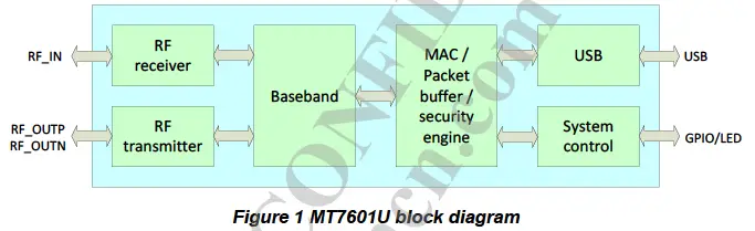
Block Diagram

Product Descriptions
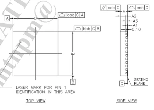
Pin Layout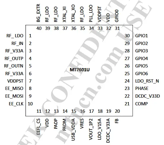 Figure 2 Top view of MT7601U QFN pin-put.
PIN Description
| QFN40 | Pin Name | Pin description | Default PU/PD | I/O | Supply domain |
| Reset and clocks | |||||
| 24 | LDO_RST N | External system reset active low | N/A | Input | VDDPST |
| 37 | XTAL_Xl | Crystal input or external clock input | N/A | Input | |
| 36 | XTAL_XO | Crystal output | N/A | Input | |
| USB interface | |||||
| 15 | USB_VDDA | USB 3.3V power supply | N/A | ||
| 16 | VRES | USB BG reference | N/A | ||
| 13 | PADP | USB D+ signal | N/A | In/out | USB_VDDA |
| 14 | PADM | USB D- signal | N/A | In/out | USB_VDDA |
| EEPROM/flash interface | |||||
| 8 | EE_MISO | External memory data input I Antenna select | PD | Input | VDDPST |
| 9 | EE_MOSI | External memory data output I Antenna select | PD | Output | VDDPST |
| 10 | EE_CLK | External clock | PU | Output | VDDPST |
| 11 | EEFL_CS | External chip select | PU | Output | VDDPST |
| Programmable I/O | |||||
| 31 | GPIOO | Programmable input/output / Bluetooth coexistence | PD | In/out | |
| 30 | GP101 | Programmable input/output! Bluetooth coexistence | PD | In/out | VDDPST |
| 29 | GPIO2 | Programmable input/output | PD | In/out | VDDPST |
| 28 | GPIO3 | Programmable input/output / Bluetooth coexistence | PD | In/out | VDDPST |
| 27 | GPIO4 | Programmable input/output / Bluetooth coexistence | PD | In/out | VDDPST |
| 26 | GPIOS | Programmable input/output | PD | In/out | VDDPST |
| 25 | GPIO6 | Programmable input/output | PD | In/out | VDDPST |
| WIFI radio interface | |||||
| 40 | BG_EXTR | RF BG reference | N/A | ||
| 2 | RF_IN | RF auxiliary RX input | N/A | ||
| 4 | RF_OUTP | RF port | N/A | ||
| 5 | RF_OUTN | RF port | N/A
| ||
| PMU/SMPS | |||||
| 17 | VOUT_1P2 | LDO 1.2V output | N/A | Output | |
| 18 | LDO_V15A | SMPS 1.5V input | N/A | iutput | |
| 19,22 | DCDC_V33 | SMPS 3.3V power supply | N/A | Input | |
| 20 | FB | SNIPS control | N/A | ||
| 21 | COMP | SMPS control | N/A | ||
| 23 | PHASE | SMPS control | N/A | ||
| Power supplies | |||||
| 7,33 | VDDPST | Digital VO power supply | N/A | Input | |
| 12,32 | VDD | Digital core power supply | N/A | Input | |
| 3,6 | RF_V33A | RF 3.3V power supply | N/A | Input | |
| 1,35, 38,39 | RF —LDO | RF power supply | N/A | Input | |
| 34 | PLL LDO | RF power supply | N/A | Input | |
| E-PAD | DVSS | Digital ground | NIA | ||
Table 1 pin descriptions
Strapping option
| QFN40 | Pin Name | Pin description | Default PU/PD | I/O | Supply domain |
| 8 | EE_MISO | XTAL_20_SEL XTAL is 20MHz: Pull up XTAL is 40MHz: Pull down | PD | ||
| 27 | GPIO4 | EXT_EE SEL: Pull down | PD | ||
| 25 | GPIO6 | CHIP_MODE[2]: Pull down | PD | ||
| 10 | EE_CLK | CHIP_MODE[1]: Pull down | PD | ||
| 9 | EE_MOSI | CHIP_MODE[0]: Pull up | PU |
Package Information
QFN Packaging


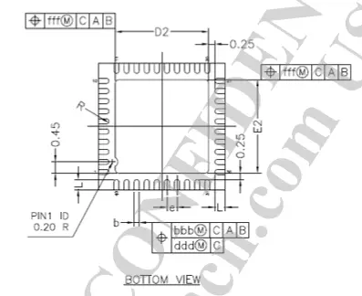
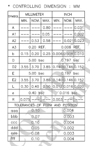
NOTES :
1ALL DIMENSIONS ARE IN MILLIMETERS.
2.DIE THICKNESS ALLOWABLE IS 0.305 mm MAXIMUM(.012 INCHES MAXIMUM)
3.DIMENSIONING & TOLERANCES CONFORM TO ASME Y14.5M. -1994.
4.THE PIN #1 IDENTIFIER MUST BE PLACED ON THE TOP SURFACE OF THE PACKAGE BY USING INDENTATION MARK OR OTHER FEATURE OF PACKAGE BODY.
5.EXACT SHAPE AND SIZE OF THIS FEATURE IS OPTIONAL.
6.PACKAGE WARPAGE MAX 0.08 mm. 7.APPLIED FOR EXPOSED PAD AND TERMINALS. EXCLUDE EMBEDDING PART OF EXPOSED PAD FROM MEASURING.
8APPLIED ONLY TO TERMINALS.
Figure 3 Package outline drawing
MediaTek Confidential
© 2012 MediaTek Inc.
This document contains information that is proprietary to MediaTek Inc.
Unauthorized reproduction or disclosure of this information in whole or in part is strictly prohibited.
Ordering Information
| Part number | Package | Operational temperature range |
| MT7601UN/A-L | 5x5x0.8 mm 40-QFN | -10~70oC |
TOP Marking Information
MTK
MT7601UN
DDDD-####
BBBBBBB
MT7601UN : Part number
DDDD : Date code
#### : Internal control code
BBBBBBB : Lot number
Figure 4 Top marking
Electrical characteristics
Absolute maximum rating
| Symbol | Parameters | Maximum rating | Unit |
| VDD33 | 3.3V Supply Voltage | -0.3 to 3.6 | V |
| VDD12 | 1.2V Supply Voltage | -0.3 to 1.5 | V |
| VDD15 | 1.5V Supply Voltage | -0.3 to 1.8 | V |
| TSTG | Storage Temperature | -40 to +125 | °C |
| VESD | ESD protection (HBM) | 2000 | V |
Table 4 Absolute maximum ratings
Recommended operating range
| Symbol | Rating | MIN | TYP | MAX | Unit |
| VDD33 | 3.3V Su.. Voltage | 2.97 | 3.3 | 3.63 | V |
| VDD12 | 1.2V Su Voltage | 1.14 | 1.2 | 1.26 | V |
| VDD15 | 1.5V SupplyI Voltage | 1.425 | 1.5 | 1.575 | V |
| TAMBIENT | Ambient Temperature | -10 | – | 70 | °C |
Table 5 Recommended operating range
DC characteristics
| Symbol | Parameter | Conditions | MIN | MAX | Unit |
| VIL | Input Low Voltage | LVTTL | -0.28 | 0.6 | V |
| VIH | Input High Voltage | 2.0 | 3.63 | V | |
| VT- | Schmitt Trigger Negative Going Threshold Voltage | LVTTL | 0.68 | 1.36 | V |
| VT+ | Schmitt Trigger Positive Going Threshold Voltage | 1.36 | 1.7 | V | |
| VOL | Output Low Voltage | |IOL| = 1.6-14 mA | -0.28 | 0.4 | V |
| VOH | Output High Voltage | |IOH| = 1.6-14 mA | 2.4 | VDD33+0.33 | V |
| RPU | Input Pull-Up Resistance | PU=high, PD=low | 40 | 190 | KΩ |
| RPD | Input Pull-Down Resistance | PU=low, PD=high | 40 | 190 | KΩ |
Table 6 DC description
Thermal characteristics
| Symbol | Description | Performance | |
| TYP | Unit | ||
| TJ | Maximum Junction Temperature (Plastic Package) | 125 | °C |
| Junction to ambient temperature thermal resistancerm[1][2] | 48.11 | °C/VV | |
| Junction to case temperature thermal resistance | TBD | °C/VV | |
| Junction to the package themal resistance[3] | 3.23 | °C/VV | |
Note :
[1] Airflow condition: Natural convection. 0.5m/s
[2] PCB dimension 21mm x 11mm.4-layer.
[3] 5mm x 5mm QFN 40l package
Tabel 7 Thermal information
Current consumption
Description | Performance | |
| TYP | Unit | |
| Sleep mode | 1.1 | mA |
| RX Active, HT40, MCS7 | 151 | mA |
| RX Power saving, DTIM=1 | 15 | mA |
| RX Listen | 6 | mA |
| TX HT40, MCS7 @15dBm | 210 | mA |
| TX CCK, 11Mbps @19dBm | 242 | mA |
Note: All result is measured at the antenna port and VDD33 is 3.3V
Table 8 WLAN 2.4GHz Current Consumption
SymbolParameterConditionsMINMAXUnitVILInput Low VoltageLVTTL-0.280.6VVIHInput High Voltage
2.03.63VVT-Schmitt Trigger Negative Going Threshold VoltageLVTTL0.681.36VVT+Schmitt Trigger Positive Going Threshold Voltage1.361.7VVOLOutput Low Voltage|IOL| = 1.6-14 mA-0.280.4VVOHOutput High Voltage|IOH| = 1.6-14 mA2.4VDD33+0.33VRPUInput Pull-Up ResistancePU=high, PD=low40190KORPDInput Pull-Down ResistancePU=low, PD=high40190KO
 ESD CAUTION
MT7601 is ESD (electrostatic discharge) sensitive device and may be damaged with ESD or spike voltage. Although MT5931 is with built-in ESD protection circuitry, please handle with care to avoid the permanent malfunction or the performance degradation.
MEDIATEK MT7601U Preliminary Datasheet – Download


 Ble Combo Card User Guide")

 Bt/ble Combo Card User Guide")


 Bt/ble Combo Card Installation Guide")


