![]()
INSTALLATION AND OPERATION
USER MANUAL
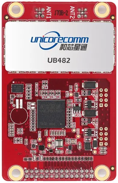
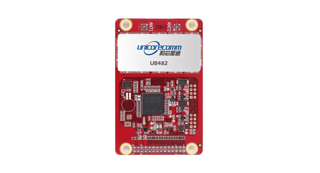
UB482
GPS/BDS/GLONASS/Galileo
All-constellation Multi-frequency
High Precision Heading Board
WWW.UNICORECOMM.COM
Revision History
| Version | Revision History | Date |
| Ver. 1.0 | First release | Aug. 2017 |
| R3.1 | Add the related description to clarify the VCC restrictions | 2019-08-28 |
| R3.2 | Chapter 2.1: revise the mechanical dimensions of fields and the RF connector Chapter 2.2: pin 12 and pin 24 are reserved | 2019-10-14 |
| R3.3 | Update product diagram and Copyright time | 2020-04-08 |
| R3.4 | 1.2 Technical Spec: add QZSS 2.4 Electrical Specifications: revise the values of VCC/Vin_low_1/Vin_high_1/Vout_low /Vout_high | 2020-07-01 |
| R3.5 | Update BDS frequencies | 2020-10-23 |
| R4 | Revise the description of pin4 Add RF input power consumption of antennas Remove information on the MEMS device | 2021-04-01 |
| R4.1 | Fix typo in Table 6-2 and Table 6-3; Revise language in chapter 6.2 and 6.3 | 2021-07-06 |
Disclaimer
Information in this document is subject to change without notice and does not represent a commitment on the part of Unicore Communications, Inc. No part of this manual may be reproduced or transmitted in any form or by any means, electronic or mechanical, including photocopying and recording, for any purpose without the express written permission of a duly authorized representative of Unicore Communications, Inc. The information contained within this manual is believed to be true and correct at the time of publication.
© Copyright 2009-2021 Unicore Communications, Inc. All rights RSV.
Foreword
This <User Manual> provides information in the features of the hardware, the installation, specification and use of UNICORECOMM UB482 product.
This manual is a generic version. Please refer to the appropriate part of the manual according to your purchased product configuration, concerning CORS, RTK and Heading.
Readers it applies to
This <User Manual> is applied to the technicists who know GNSS Receiver to some extent but not to the general readers.
Overview
UB482 is a classic compact high-precision board developed by Unicore Communications, Inc., targeting precision agriculture, robots and intelligent driving applications. It supports all-constellation multi-frequency RTK and heading function.
The UB482 can provide reliable centimeter-level accuracy and high accuracy heading output at high update rate.
By employing a single UC4C0 (432 channel tracking) baseband chip and a single RF chip, using single-sided SMD packaging, UB482 has achieved very small size (30x40mm). It can simultaneously track GPS L1/L2 + BDS B1I/B2I + GLONASS L1/L2+Galileo E1/E5b+QZSS.
The UB482 adopts UNICORECOMM’s new-generation “UGypsophila” RTK processing technology and takes advantage of the high-performance data sharing capability and super-simplified operating system within the NebulasII GNSS SoC chip. It uses optimized multi-dimensional RTK matrix pipeline computation, resulting in much higher RTK processing capability.
1.1 Key Features
➢ All-constellation multi-frequency high-precision RTK and heading board, support BDS B1I/B2I + GPSL1/L2+GLONASS L1/L2+Galileo E1/E5b+QZSS L1/L2
➢ 46x71mm classic compact board
➢ Precise RTK positioning and heading
➢ Fast RTK Initialization time < 5s
➢ 20Hz data output rate
➢ Adaptive recognition of RTCM input data format
➢ Support LAN
➢ Support odometer input and external high-performance IMU interface*
1.2 Technical Specifications
Table 1-1 Performance Specifications
| Channels | 432 channels, based on NebulasII SoC chip | Cold Start | <25s |
| Frequency | GPS L1/L2 BDS B1I/B2I1 GLONASS L1/L2 Galileo E1/E5b QZSS L1/L2 | Initialization Time | <5s (Typical) |
| Single Point Positioning (RMS) | Horizontal: 1.5m Vertical: 2.5m | Initialization Reliability | >99.9% |
| DGPS (RMS) | Horizontal: 0.4m Vertical: 0.8m | Differential Data | RTCM 3.0/3.2/3.3 |
| Data Formats | NMEA-0183, Unicore binary | ||
| RTK (RMS) | Horizontal: 1cm+1ppm Vertical: 1.5cm+1ppm | Update Rate | 20Hz |
| Time Accuracy (RMS) | 20ns | ||
| Heading Accuracy (RMS) | 0.2 degree/1m baseline | Data Accuracy (RMS) | 0.03m/s |
| Size | 46x71x10mm | Power Consumption | 2.4W (Typical) |
Functional Ports
| 3x UART, 1xI2C, 1x SPI (LV-TTL) | 1x LAN |
| 1x Event input | 1x1PPS (LV-TTL) |
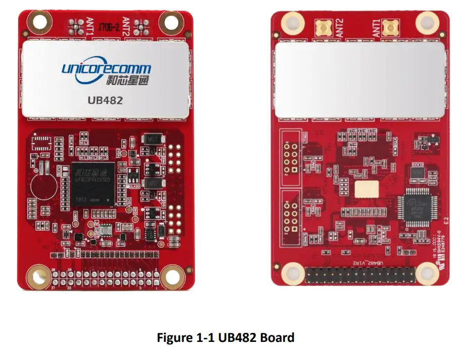
1.3 Board Overview
- RF Part
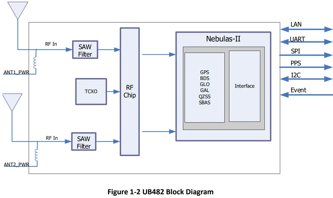
The receiver gets filtered and enhanced GNSS signal from the antenna via a coaxial cable. The RF part converts the RF input signals into the IF signal, and converts IF analog signal into digital signals required for NebulasII (UC4C0) digital processing.
NebulasII SoC (UC4C0)
The UB482 incorporates the processing from the NebulasII (UC4C0), UNICORECOMM’s new generation high precision GNSS SoC with 55nm low power design, which supports up to 12 digital intermediate frequency or 8 analog intermediate frequency signals and can track 12 navigation signals with 432 channels. - 1PPS
UB482 outputs 1 Pulse-per-second time strobe with corresponding time and positioning tag. The pulse width/polarity is configurable. - Event
UB482 provides 1 Event Mark Input with adjustable pulse width and polarity. - Reset (RESETIN_N)/Factory Default (FRESET_N)
The reset signal RESETIN_N should be set active low, no less than 5ms effective time.
When the FRESETN_N is activated, the user parameter in NVM will be cleared and the board is restored to factory default settings. The FRESET_N is active low. Please pull FRESET_N pin to low level for more than 5s to ensure successful reset.
Hardware
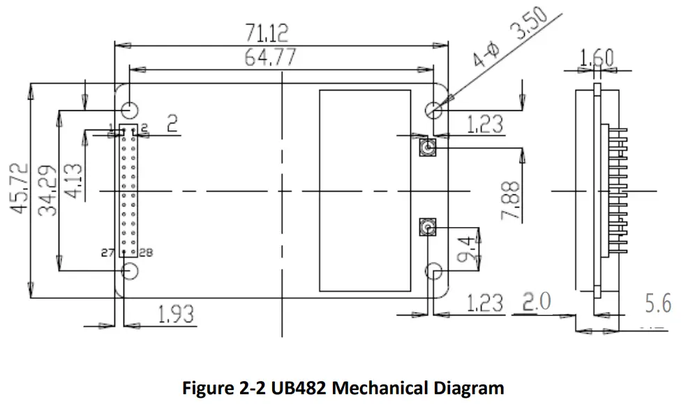
2.1 Dimensions
Table 2-1 Dimensions
| Parameter | Value | Tolerance |
| Length | 71.1mm | -0.2mm +0.5mm |
| Width | 45.7mm | ±0.2mm |
| Height (PCB) | 1.6mm | ±10% |
| RF Connector | 4.5mm | ±0.2mm |
| Shield | 2.0mm | ±0.2mm |
| Pin Distance | 5.9mm | ±0.2mm |
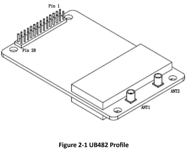
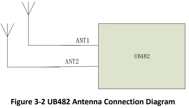
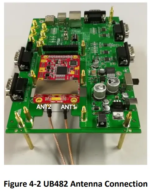
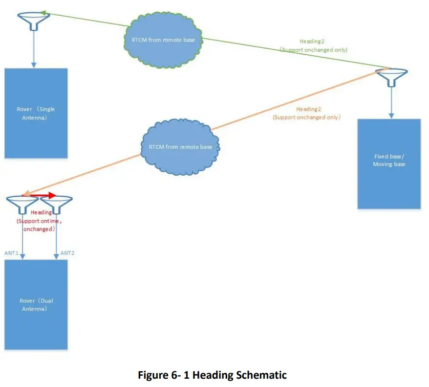
ANT1 is the primary antenna (positioning) and ANT2 is the secondary antenna (heading). The antenna is MMCX connector. When working as a base station, only ANT1 should be connected. When working as a rover, the direction output is the result of the anticlockwise angle between the vector (starting from ANT1, ending at ANT2) and True North.
2.2 Connector and Pin Definition
There are two dual rows of pin headers on UB482: 2×14 dual row, 2.0mm pitch
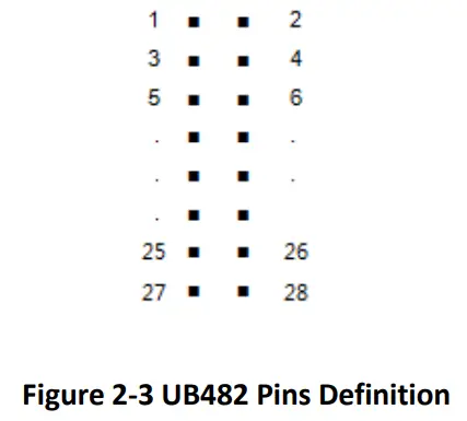
Note: The model number of the dual row pin header (28pin male) on the UB482 board is: CH71283V100 from CviLux. It’s recommended to mate with the Molex’s plug-in socket (28Pin female), of which the model number is: 79107-7013.
2.3 Pins Function Description
Table 2-2 Pins Function
| Pin | Signal | I/O | Description | Notes |
| 1 | SPI_MOSI | O | SPI data | Master output, Slave input |
| 2 | SPI_CS | O | SPI chip select | |
| 3 | SPI_CLK | O | SPI clock | |
| 4 | TPO_MID | O | Ethernet transformer center tap | Connect Center Tap |
| 5 | RSV | – | Reserved | |
| 6 | VCC | Power | Power input | 3.3V~5VDC |
| 7 | SPI_MISO | I | SPI data | Master input, Slave output |
| 8 | RXD3 | I | COM3 input data reception | LVTTL |
| 9 | RESETIN_N | I | Reset input | LVTTL, low active (>5ms) |
| 10 | FRESET_N | I | Restore to factory default setting (user configuration will be reset) | LVTTL, low active (> 5s) |
| 11 | EVENT | I | Event input | LVTTL |
| 12 | RSV | – | Reserved | |
| 13 | TXD3 | O | COM3 output transmit data | LVTTL |
| 14 | GND | Power | ||
| 15 | TXD1 | O | COM1 output transmit data | LVTTL |
| 16 | RXD1 | I | COM1 input data reception | LVTTL |
| 17 | GND | Power | ||
| 18 | TXD2/SDA | O | COM2 output transmit data/or I2C SDA | LVTTL |
| 19 | RXD2/SCL | I | COM2 input data reception /or I2C SCL | LVTTL |
| 20 | GND | Power | ||
|
21 | PV | O | Position valid | High effective (RTK fix is effective when UB482 works as the rover; When UB482 works as the base station, successfully set up the base station and GPGGA status bit is “7”, the pin is effective). If LED indicator is needed, lead the pin to the anode of the LED diode. |
| 22 | GND | Power | ||
| 23 | PPS | O | Pulse per second |
| 24 | RSV | – | Reserved | |
| 25 | TPO+ | O | Positive electrode of Ethernet sending data, Differential pair. | Connect to TD+ |
| 26 | TPI+ | I | Positive electrode of Ethernet receiving data, Differential pair | Connect to RD+ |
| 27 | TPO- | O | Negative electrode of Ethernet sending data, Differential pair | Connect to TD- |
| 28 | TPI- | I | Negative electrode of Ethernet receiving data, Differential pair | Connect to RD- |
2.4 Electrical Specifications
Table 2-3 Absolute Maximum Rating
| Item | Pin | Min | Max | Unit |
| Power Supply (VCC) | Vcc | -0.3 | 5.5 | V |
| Voltage Input | Vin | -0.3 | 3.6 | V |
| VCC Ripple (Rated Max.) | Vrpp | 0 | 50 | mV |
| Voltage Input (pins other than RXD1, RXD2, RXD3) | Vin | -0.3 | 3.6 | V |
| RF Input Power Consumption of master antenna | ANT1_IN input power | +15 | dBm | |
| RF Input Power Consumption of slave antenna | ANT2_IN input power | +15 | dBm | |
| Maximum ESD stress | VESD (HBM) | ±2000 | V |
2.5 Operational Conditions
Table 2-4 Operational Conditions
| Item | Pin | Min | Typical | Max | Unit | Condition |
| Power Supply (VCC) | Vcc | 3.3 | 3.3 | 5.0 | V | |
| Inrush Current2 | Iccp | 10 | A | Vcc = 3.3 V | ||
| LOW Level Input Voltage | Vin_low_1 | -0.3 | 0.9 | V | ||
| High Level Input Voltage | Vin_high_1 | 2.4 | 3.6 | V | ||
| LOW Level Output Voltage | Vout_low | 0 | 0.45 | V | Iout= 4 mA |
2 Since the product has capacitors inside, inrush current will occur during power-on. Evaluate in the actual
environment in order to check the effect of the supply voltage drop due to the inrush current.
| Item | Pin | Min | Typical | Max | Unit | Condition |
| High Level Output Voltage | Vout_high | 2.85 | 3.3 | V | Iout =4 mA | |
| Antenna Gain | Gant | 20 | 36 | dB | ||
| Power Consumption | P | 2.3 | 2.6 | W |
2.6 Physical Specifications
Table 2-5 Physical Specifications
| Temperature | Operating: -40℃~+85℃ |
| Storage: -55℃~+95℃ | |
| Humidity | 95% No condensation |
| Vibration | GJB150.16-2009, MIL-STD-810 |
| Shock | GJB150.18-2009, MIL-STD-810 |
Hardware Design
3.1 Design in Considerations
- The module’s VCC should be monotonic when powered on, the initial level should be lower than 0.4V, and the undershoot and ringing should be guaranteed to be within 5% VCC
- ANT1 and ANT2 MMCX interfaces supply DC 4.8~5.4 V feed in no-load condition, and supply DC 4.6V±0.2V feed when the working circuit is 30~100mA tested in room temperature. Fifty (50) ohm impedance matching for ANT1 and ANT2 is strongly recommended
- Supply stable power to the VCC pin. Connect all the GND pins to ground
- Ensure COM1 is connected to the host. COM1 is required for firmware upgrades.
- FRESET_N resets the factory settings for the board. RESETIN is fast reset; please ensure the board is connected correctly to reset the board.
In order to obtain proper performance, special concerns should be paid during the design to the following:
- Power supply: A stable and low ripple power supply is necessary for good performance. Make sure the peak to peak voltage ripple does not exceed 50mVpp. It is recommended to use a power chip with current output capacity greater than 2A to power the board.
− Use LDO to ensure the purity of the power supply
− Try to place LDO close to the module in layout
− Widen the tracks of power circuit or use copper pour surface to transmit current
− Avoid walking through any high-power or high inductance devices such as a magnetic coil - Interfaces: Ensure that the signals and baud rate of the main equipment match those of the UB482 board
- Antenna interface: Make sure the antenna impedance matches, and the cable is short without any kinks, try to avoid acute angles
- Try to avoid designing in any circuits underneath UB482
- Keep the board away from any high temperature air flow as far as possible
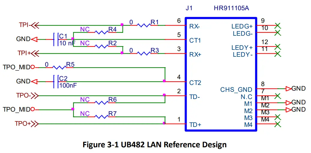
3.2 UB482 Reference Design
The reference design of UB482 LAN is as follow:
Note:
R2, R4, R6 and R7 are reserved for impedance matching. Generally, no soldering is required.
3.3 Pins
| Pin/Connector | I/O | Description | Notes | |
| Power Supply | VCC | power | Voltage Supply | Stable, clean low ripple power supply, peak ripple power lower than 50mVpp is preferred |
| ANT1/ANT2 MMCX | power | Antenna Power Supply | Voltage supply for active antenna. When the antenna interface of the module connects no antennas, the voltage tested by multimeter is DC 4.8~5.4 V; When the RF interface of the module connects an antenna and the working circuit is tested as 30~100 mA under room temperature, |
| the voltage is DC 4.6V±0.2V | ||||
| GND | power | Ground | Connect all the GND signals to ground. Better use copper pour surface. | |
| UART | TXD1 | O | COM1 Transmit Data | COM1 output, leave unconnected if not used |
| RXD1 | I | COM1 Receive Data | COM1 input, leave unconnected if not used | |
| TXD2 | O | COM2 Transmit Data | COM2 output, leave unconnected if not used | |
| RXD2 | I | COM2 Receive Data | COM2 input, leave unconnected if not used | |
| TXD3 | O | COM3 Transmit Data | COM3 output, leave unconnected if not used | |
| RXD3 | I | COM3 Receive Data | COM3 input, leave unconnected if not used | |
| System | FRESET_N | I | Hardware Reset | FRESET_N requires more than 5s to reset the board to factory default. Don’t connect it if not used |
| RESETIN_N | I | Hardware Reset | External reset signal, low active, keep that more than 5ms. Don’t connect it if not used |
3.4 Antenna
The ANT1 and ANT2 MMCX are connected to active antennas directly and supply feed for the antenna. When the antenna interfaces of ANT1 and ANT2 connect no antennas, which means there is no load, the voltage tested by multimeter is DC 4.8~5.4 V; When the RF interface of the module connects an antenna and the working circuit is tested as 30~100 mA in room temperature, the voltage is DC 4.6V±0.2V. Fifty (50) ohm impedance matching for ANT1 and ANT2 is strongly recommended when the active antenna is connected.
Installation and Configuration
4.1 ESD Handling Precautions
UB482 Board is an ESD sensitive device and special precautions when handling are
required.
- Electrostatic discharge may cause damages to the device. All operations mentioned in this chapter should be carried out on an antistatic workbench,
wearing an antistatic wrist strap and using a conductive foam pad - Hold the edge of the board, and do NOT directly touch the electronic components
4.2 Installation Guide
The user may assemble UB482 flexibly according to the application scenarios and market needs. The following figure shows a typical installation of the UB482 using the Evaluation Kit (EVK).
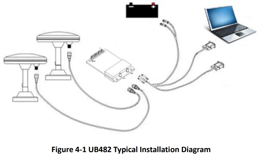
Please inspect the shipping cartons for any signs of damage or mishandling before unpacking the UB482 package. The following items are required to install the UB482 board correctly:
- UB482 EVK suite (or evaluation board)
- User manual
- UPrecise software
- Qualified antenna
- MMCX antenna cable
- A PC or laptop with serial ports (Win7 and above), with UPrecise installed
Follow the steps below to install:
➢ Step 1: Fix UB482 board on the EVK with the holes and pins accurately.
➢ Step 2: Choose the correct location for the antenna—this is critical for a highquality installation. Poor or incorrect placement of the antenna can influence accuracy and reliability and may result in damage during normal operation. Use the coaxial radio frequency cable to connect the antenna connector of B482 EVK;
Note:
The RF connector on the board is MMCX, and the suitable connecting wire should be selected according to the package. The input signal gain at the antenna interface is optimal between 20 and 36dB. Please select the appropriate antenna, antenna cable and online LNA accordingly.
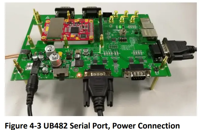
➢ Step 3: Connect the PC to the EVK serial port through direct serial cable;
➢ Step 4: Connect a 12V adapter to the EVK power input, and switch on the EVK;
➢ Step 5: Open the UPrecise software on the PC;
➢ Step 6: Configure the receiver through UPrecise software to send commands or log data.
4.3 Power On
UB482 power supply voltage is 3.3V. After power-on, the receiver starts and can establish communication quickly.
4.4 Configuration and Output
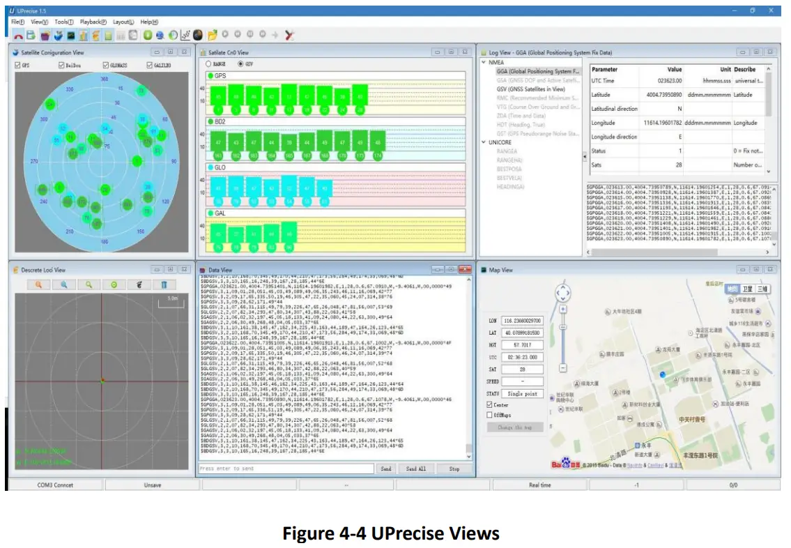
UNICORECOMM UPrecise software provides graphical interface to control and display the operation of the receiver. The features of UPrecise software include:
- Connecting and configuration of the receiver
- Constellation View: Graphic window to display Position of satellite, PRN, and Signal/Noise Ratio
- Trajectory View: The trajectory view for displaying the present point and the past point of the Receiver
- Logging Control View: Graphic interface for data logging
- Console View: Console window for sending command to the receiver
- Upgrading the firmware
- TTFF test
4.4.1 Operation Steps
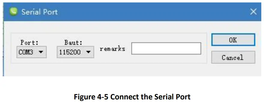
- Turn on the EVK. Click “file – > connect”. Set the baud rate: the default baud rate is 115200 bps
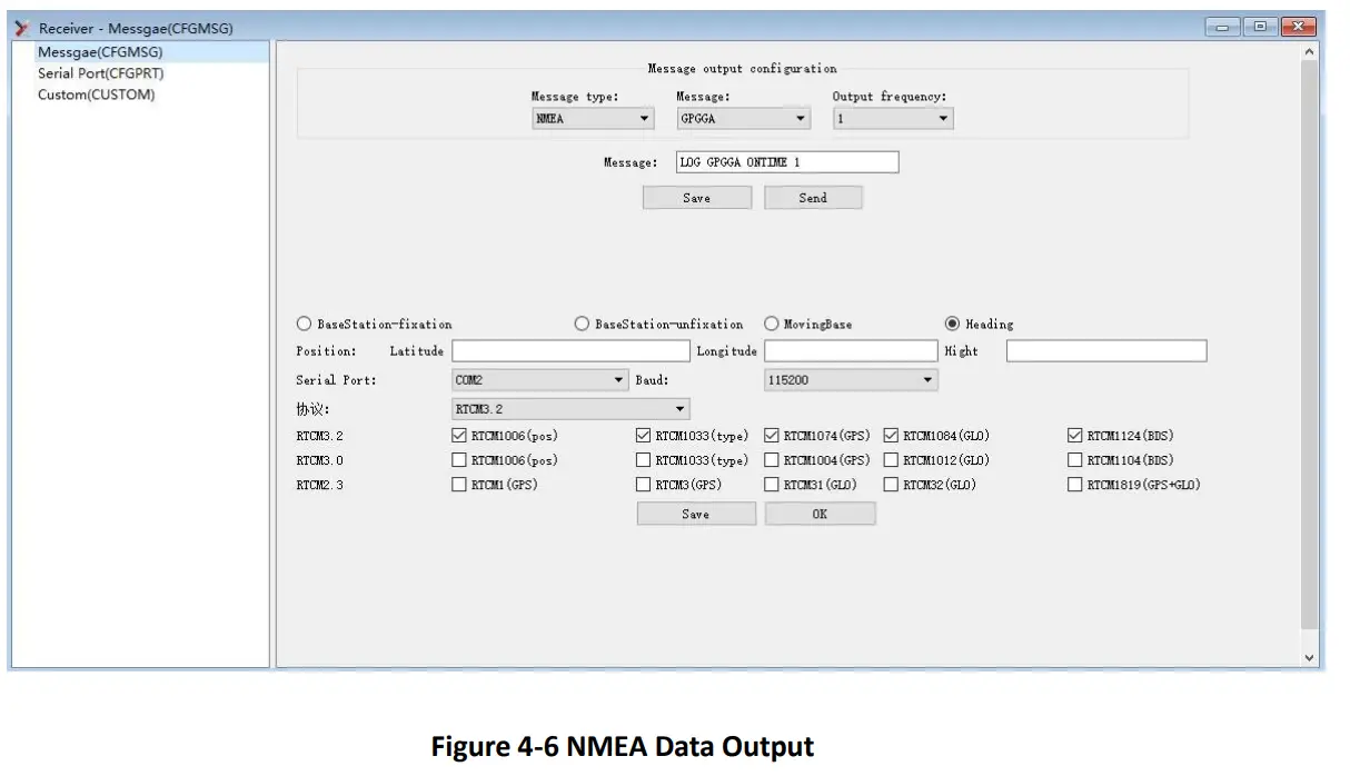
- Click the “receiver settings” button to configure the NMEA message output
- Click “send” button. It is recommended to configure GPGGA, GPGSV, and other messages. Or in the dialog window, click on “Send all Message” to complete all the NMEA message output (default update rate 1Hz).
- In the data session window right click to adjust output log font size, to stop / resume log output, or to clear log content
- Configure or type commands using the UPrecise view.
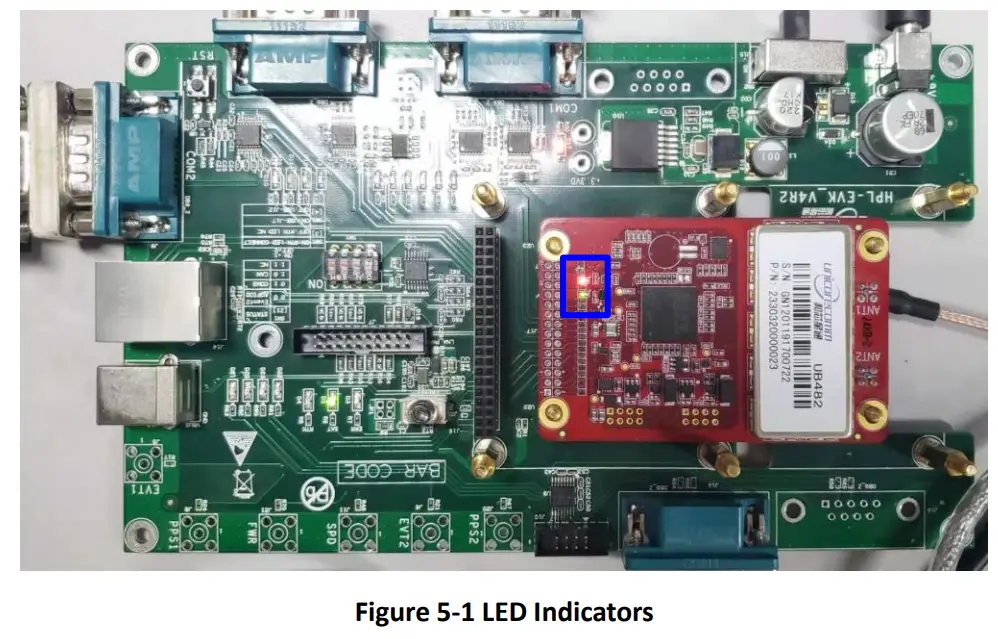
LED Indicators
LED indicators are installed on UB482 board to indicate the basic working status of the board, which includes:
| No | Color | Status | Instruction | Remark |
| 1 | Red | On | Power on | |
| 2 | Off | Power off | ||
| 3 | Green | On | Valid of RTK fix when UB482 works as the rover | |
| 4 | Off | Invalid of RTK fix when UB482 works as the rover |
The LED indicators are shown in the following figure:
Configuration Commands
UB482 supports abbreviated ASCII format. All commands are composed of a log heading and configuration parameters.
Common instructions are shown in the following table:
Table 6-1 Common Instructions
| Command | Description |
| freset | Reset to factory settings. Note: the factory set baud rate is 115200 bps. |
| version | Query the hardware version, firmware version of receivers |
| config | Current configuration of each port of the receiver |
| mask BDS | Mask (disable) tracking of Beidou satellite system. BDS, GPS, GLONASS and Galileo can be disabled separately |
| unmask BDS | Unmask (enable) tracking of Beidou satellite system. BDS, GPS, GLONASS and Galileo can be enabled separately. By default, all satellite systems are tracked. |
| config com1 115200 | Set the baud rate of com1 to 115200. Baud rates of com1, com2 and com3 can be set to any of the following: 9600, 19200, 38400, 57600, 115200, 230400,460800 |
| unlog | Disable all output of the current port |
| saveconfig | Save configuration to NVM (nonvolatile memory) |
| mode base time 60 1.5 2.5 | Derive an average coordinate after 60 seconds or when a “better than 1.5 meter horizontal and less than 2.5 meter height accuracy” is achieved within 60 seconds. When restarting after power off, the calculations will repeat and a new coordinate will be generated. |
| Command | Description |
| mode base lat Lon height | Mode base lat Lon height: Manually configure the coordinate: lat, lon, height Example: lat=40.07898324818, lon=116.23660197714, height=60.4265 Note: The latitude and longitude coordinates can be obtained through command bestpos. Lat or lon Negative means the location is in the southern hemisphere or in the western hemisphere |
| mode base | Config as base station |
| mode movingbase | Config as moving base |
| mode rover | Config as rover (default mode) |
| rtcm1033 comx 10 rtcm1006 comx 10 rtcm1074 comx 1 rtcm1124 comx 1 rtcm1084 comx 1 rtcm1094 comx 1 | Set port X to send differential message under base station mode. X could be either com1, com2, or com3. |
| NMEA0183 Output Message | |
| gpgga comx 1 | Output GGA in 1Hz. Output data rate could be: 1, 0.2, 0.1, corresponding to 1hz, 5hz, 10hz; Message types could be GGA, RMC, ZDA, VTG, NTR |
| gphdt comx 1 | Output current heading information Heading information includes: HDT, TRA |
6.1 Reference Station Configuration
The RTK base station is static with a fixed and known position. The common instructions to set up an RTK base station configuration are:
1) If the precise coordinates are known, the precise coordinates could be set as in this example:
Table 6-2 Base Station Mode
| No | Command | Description |
| 1 | mode base 40.078983248 116.236601977 60.42 | Set latitude, longitude, and |
| 2 | rtcm1006 com2 10 | Reference station coordinate (including antenna height) |
| 3 | rtcm1033 com2 10 | Receiver and antenna description |
| 4 | rtcm1074 com2 1 | GPS correction data |
| 5 | rtcm1124 com2 1 | BDS correction data |
| 6 | rtcm1084 com2 1 | GLONASS correction data |
| 7 | rtcm1094 com2 1 | Galileo differential correction data |
| 8 | saveconfig | Save configuration |
2) Self-Optimizing Base Station Mode: If there are no precise coordinates already available, select auto-fix option and the receiver will work for a certain period, and will then use the derived value as the base station coordinates. The most usual instructions are as follow:
Table 6-3 Self-Optimizing Base Station Mode
| No | Command | Description |
| 1 | mode base time 60 1.5 2.5 | Within 60 seconds of the automatic positioning of the receiver, or when the standard deviation of horizontal positioning is no more than 1.5 m and that of vertical positioning is no more than 2.5 m, set the average value of horizontal and vertical positioning results as the fixed base station coordinates. |
| 2 | rtcm1006 com2 10 | Reference station coordinates, including the antenna height |
| 3 | rtcm1033 com2 10 | receiver and antenna description |
| 4 | rtcm1074 com2 1 | GPS correction data |
| 5 | rtcm1124 com2 1 | BDS correction data |
| 6 | rtcm1084 com2 1 | GLONASS correction data |
| 7 | rtcm1094 com2 1 | Galileo differential correction data |
| 8 | saveconfig | Save configuration |
6.2 Rover Station Configuration
The RTK rover receives the differential correction data from the base station and synchronously receives satellite signals to process an RTK solution, and finally RTK high precision heading becomes available. Common instructions to set up the rover stations are as follows:
MODE ROVER
GNGGA 1
SAVECONFIG
6.3 Moving Base Configuration
Different from RTK base station which has a fixed position, the moving base station is in motion and sends differential correction data to the receiver of the rover station.
UB482 can adaptively recognize RTCM data input interface and format. Frequently used instructions to set up the moving base stations are as follows:
Table 6-4 Moving Base Station Mode
| No | Command | Description |
| 1 | mode movingbase | Set the moving base station mode |
| 2 | rtcm1006 com2 1 | Base station antenna coordinates (include antenna height) |
| 3 | rtcm1033 com2 1 | Description of receiver and antenna |
| 4 | rtcm1074 com2 1 | GPS system correction data |
| 5 | rtcm1124 com2 1 | BDS system correction data |
| 6 | rtcm1084 com2 1 | GLONASS system correction data |
| 7 | rtcm1094 com2 1 | Galileo system correction data |
| 8 | saveconfig | Save configuration |
6.4 Heading Configuration
This command is used for dual-antenna receivers (UB482, UM482, and UM442). The heading result is the angle from True North to the baseline of the ANT1 to ANT2 in a clockwise direction. The heading function is enabled by default settings. See Figure 6- 1 Heading Schematic for the schematic.
Frequently used commands are as follows:
GPHDT 1
SAVECONFIG
6.5 Heading2 Configuration
The heading2 result is the angle from True North to the baseline of the base to rover in a clockwise direction. Dual-antenna heading receiver (UB482, UM482, UM442) supports heading2. The heading2 for the dual-antenna receiver is the angle from True North to the baseline of the Base to ANT1 in a clockwise direction. Please refer to figure 6-1 for the detailed schematic.
Frequently used commands are as follows:
MODE HEADING2
GPHDT2 ONCHANGED
SAVECONFIG
Firmware Upgrade
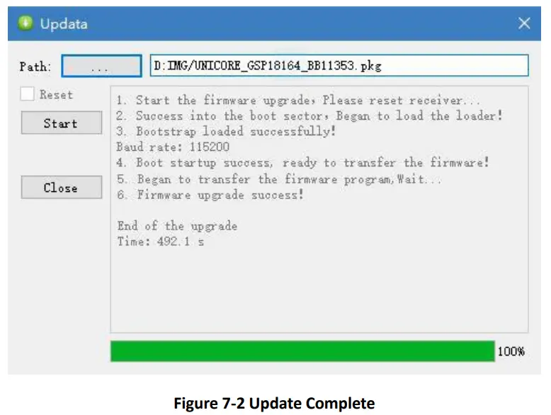
Upgrading UB482 could be done using the UPrecise software: Click “…” to browse the firmware update package, and click “Start” button to start the firmware upgrading process (don’t select “Reset” checkbox):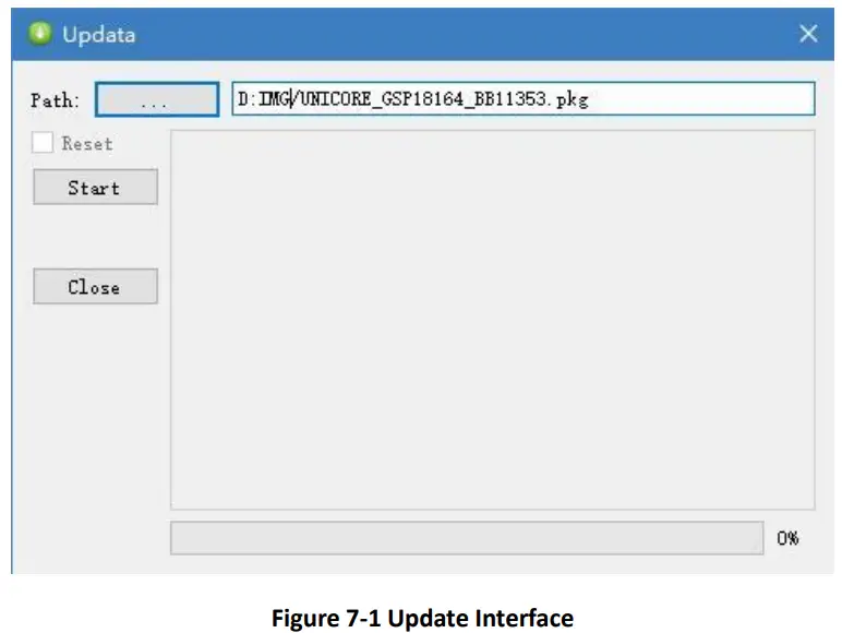 In general, the upgrade time is within 5minutes.
Note: Please use COM1 for firmware upgrade
Packaging
There are 100pcs UB482 boards inside the package box.
| No | Description |
| 1 | 10 inner boxes/cartons |
| 2 | 10 pieces of anti-static plastic bags/inner boxes (1 UB482 board/ anti-static plastic bag) |
![]()
Unicore Communications, Inc.
F3, No.7, Fengxian East Road, Haidian, Beijing, P.R.China,
100094
www.unicorecomm.com
Phone: 86-10-69939800
Fax: 86-10-69939888
[email protected]


