![]()
HDMI Display Module
AN9134
User Manual
AN9134 HDMI Display Module
Version Record
| Version | Date | Release By | Description |
| Rev1.0 | 10-11-19 | Rachel Zhou | First Release |
Part 1: HDMI Display Module General Description
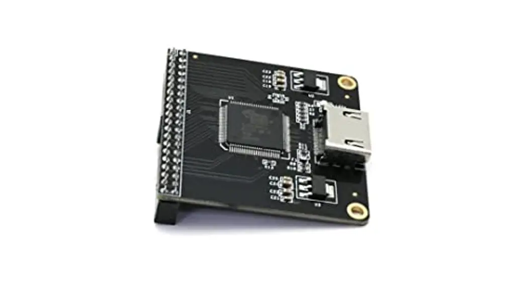
ALINX HDMI Display Output Module AN9134, use SIL9134 HDMI(DVI) coding chip of Silion Image Incorporation. Supports maximum 1080P@60Hz output and 3D output。The module reserves a 40-pin female header that to connect FPGA development kit, a HDMI connector that to output HDMI video signal to HMDI Monitor Figure 1-1: AN9134 module product photo as below:
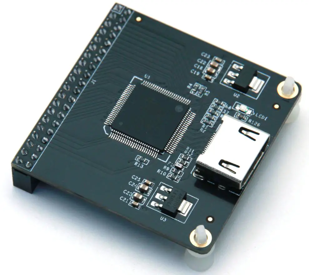
Figure 1-1: AN9134 module product photo
AN9134 Module Detail Parameter
HDMI display module detail parameter listed in below:
- HDMI coding chip:SiI9134
- HDMI display channel:1-channel
- HDMI interface display standard:HDMI 1.4
- Bus width: 24 bits RGB/YCbCr 4:4:4
- Max. Display resolution and frame rate: 1080P 60 Hz
- Display parameter configuration:I2C Interface
- Module Interface : 40-pin 0.1 spacing female header, download direction
- Ambient Temperature (with power applied):-0°~70°
- Output Interface:1-channel HDMI standard output interface
AN9134 Module Parameter Description
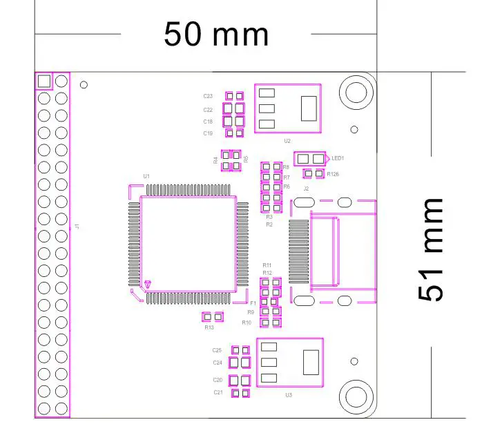
Figure 1-2: AN9134 Display Module Dimensions
Part 2: HDMI Display Module Function Description
AN9134 Module Block Diagram
Figure 2-1: AN9134 Module Block Diagram as below:
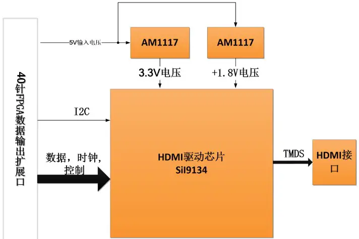
Figure 2-1: AN9134 Module Block Diagram
AN9134 Module 40-pin Female Header Pins Description
| Pin | Pin Name | Description |
| 1 | GND | Digital Ground |
| 2 | +5V | 5V power input |
| 3 | 9134_SCL | 9134 I2C clock |
| 4 | 9134_SDA | 9134 I2C data |
| 5 | 9134_D22 | bit 22 of date input to module |
| 6 | 9134_D23 | bit 23 of date input to module |
| 7 | 9134_D20 | bit 20 of date input to module |
| 8 | 9134_D21 | bit 21 of date input to module |
| 9 | 9134_D18 | bit 18 of date input to module |
| 10 | 9134_D19 | bit 19 of date input to module |
| 11 | 9134_D16 | bit 16 of date input to module |
| 12 | 9134_D17 | bit 17 of date input to module |
| 13 | 9134_D14 | bit 14 of date input to module |
| 14 | 9134_D15 | bit 15 of date input to module |
| 15 | 9134_D12 | bit 12 of date input to module |
| 16 | 9134_D13 | bit 13 of date input to module |
| 17 | 9134_D10 | bit 10 of date input to module |
| 18 | 9134_D11 | bit 11 of date input to module |
| 19 | 9134_D8 | bit 8 of date input to module |
| 20 | 9134_D9 | bit 9 of date input to module |
| 21 | 9134_D6 | bit 6 of date input to module |
| 22 | 9134_D7 | bit 7 of date input to module |
| 23 | 9134_CLK | 9134 clock signal |
| 24 | 9134_D5 | bit 5of date input to module |
| 25 | 9134_D3 | bit 3 of date input to module |
| 26 | 9134_D4 | bit 4 of date input to module |
| 27 | 9134_D1 | bit 1 of date input to module |
| 28 | 9134_D2 | bit 2 of date input to module |
| 29 | 9134_DE | date input enable signal |
| 30 | 9134_D0 | bit 0 of date input to module |
| 31 | 9134_VS | Vertical sync input control signal |
| 32 | 9134_HS | Horizontal sync input control signal |
| 33 | 9134_nRESET | Reset signal of module |
| 34 | 9134_INT | Interrupt signal of module |
| 35 | – | NC |
| 36 | – | NC |
| 37 | GND | Digital Ground |
| 38 | GND | Digital Ground |
| 39 | +3.3V | NC |
| 40 | +3.3V | NC |
Part 3 HDMI Display Module Program Description
We provide the HDMI driver programs of ALINX Series FPGA development board. In these driver demos, the FPGA drives the output display of SiI9134 by Internally generating HDMI timing and testing data. The different resolution of testing image can be generate by modifying the output clock timing of HDMI. Press the button KEY1 to switch the testing images. The function diagram of the testing programs (Figure 3-1) as below:
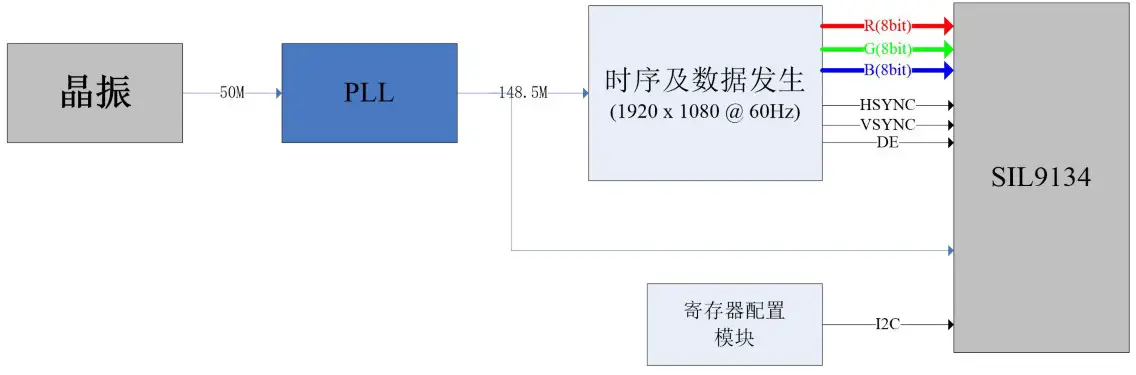
Figure 3-1: The function diagram of the testing programs
Below is the brief instruction to the functions of each module used in the FPGA driver programs
- mv_pattern.v
This module is used to generate different testing images and HDMI Vertical/ Horizontal sync signals. It generated 7 patterns testing images, included 8-color horizontal strip, 8-color vertical bar, scrolling gradient, black and white square, all blue, color gradient, frame. The Vertical/ Horizontal sync signals of HDIM generated by the parameter defined by TOP layer, that are the timing required by HDMI. - ax_debounce.v
This module is used to detect the action of press the button, detect the falling edged of button. The function of button debounce is also added in the programs. - i2c_config.v
This module is used to registers the SiI9134 chip by calling the I2C communication module , the configured register address and value are defined in the lut_9134.v file. The specific registers meaning, please refer to the instruction manual of SiI9134 chip. - reset_power_on.v
This modules is used to generate a software reset to initialize others modules after power-on.
Part 4 Hardware connection and Testing
The hardware connection between the AN9134 module and FPGA development are easy. The 40-pin female headers of module plug into the expansion board of FPGA development kit, and then connect the HDMI connector to the monitor. The figure 4-1 is the expansion IOs J1 of ALINX Series FPGA development kit AX301 and the AN9134 HDMI module hardware connection as below: (if connected to the expansion IOs J2, need to re-assign the pins)
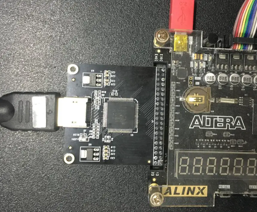
Figure 4-1: Hardware connection to ALINX Series FPGA Board
Power on the FPGA development kit, download the programs, and then the 8-color vertical bar testing image display in HDMI monitor.
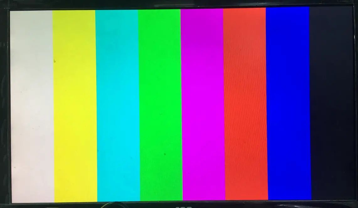
Figure 4-2: 8-color vertical bar display in HDMI monitor
Switch the testing image by press Button KEY1:
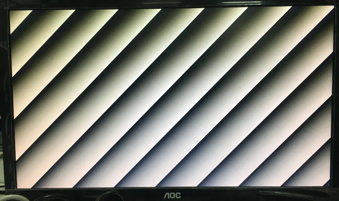
Figure 4-3: Scrolling grayscale bar display in HDMI monitor
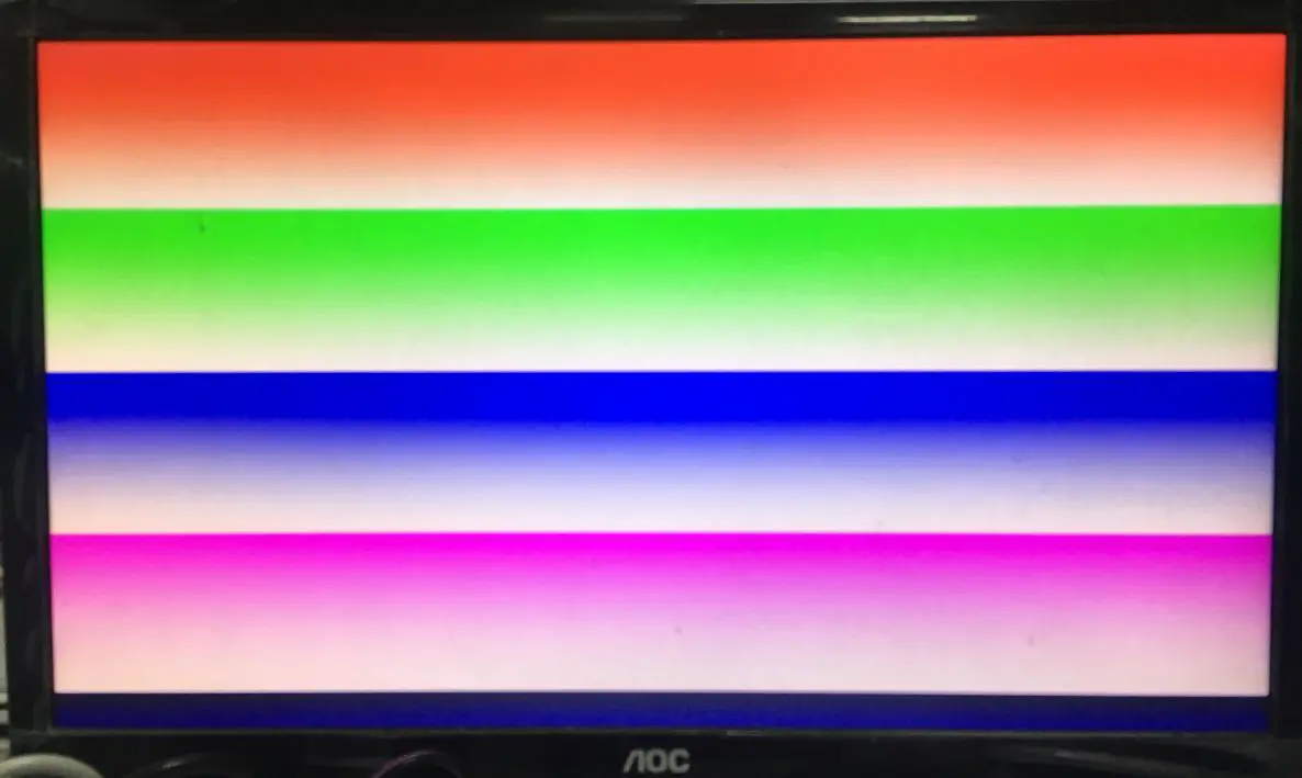
Figure 4-4: colored gray bars display in HDMI monitor
If the users to modify the output image resolution, just need to modify two places:
- an9134_test (Modify the resolution in the top file)
 Figure 4-5: Modify the resolution in top file
 - Modify the output clock frequency of PLL, the default output clock frequency is 1080P(148.5M), you need to modify the value marked in
Figure 4-6. The output clock frequency of different resolution remarked in the programs.
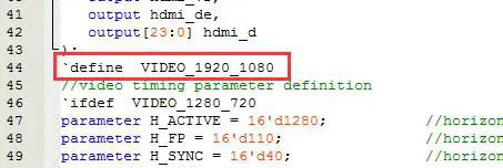 Figure 4-5: Modify the resolution in top file
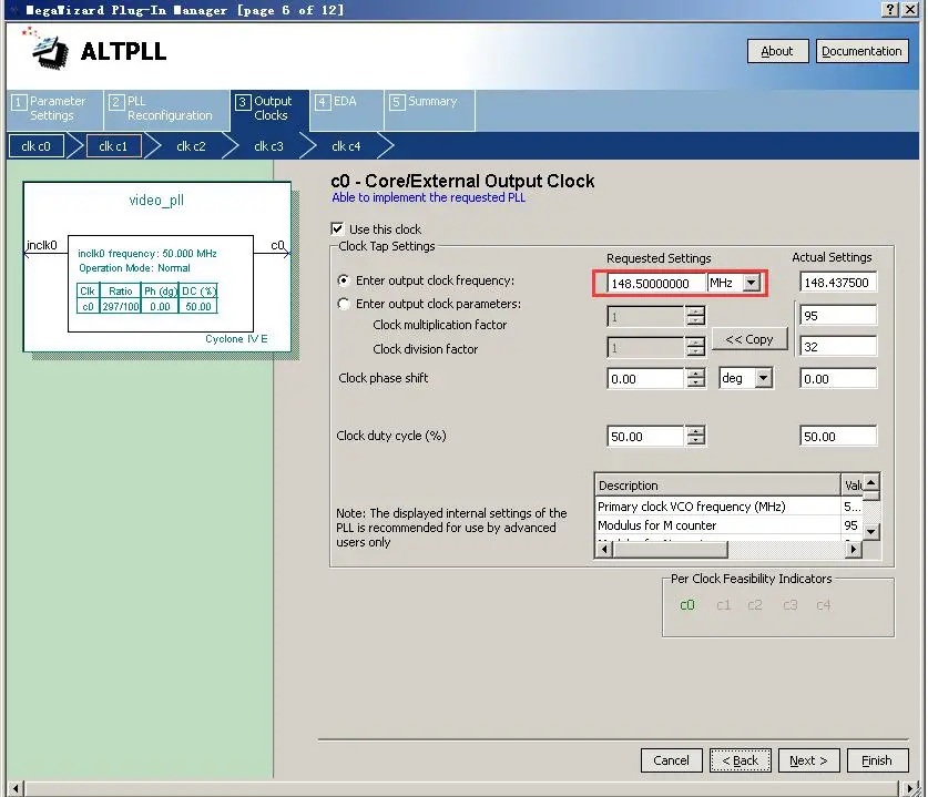
Figure 4-6: Modify the output clock frequency of PLL


