![]() FMC HDMI Display
FMC HDMI Display
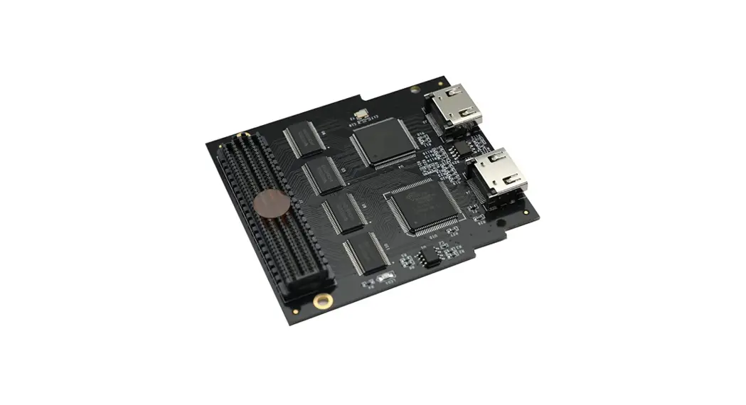
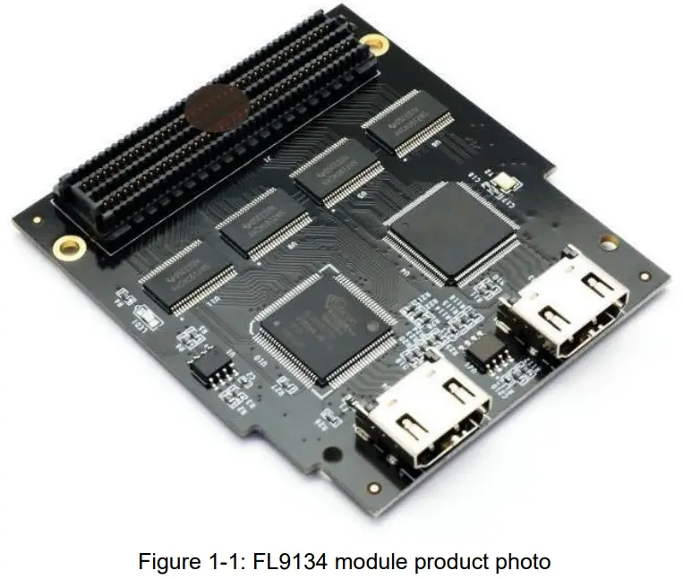
Module FL9134
User Manual
Part1: FMC HMDI Module FL9134 General Description
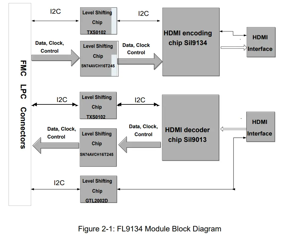
The ALINX FMC HDMI Module FL9134 includes one HDMI video input and one HDMI video output. The HDMI input uses Silicon Image’s SIL9013 HDMI decoder chip, which supports up to 1080P@60Hz input and supports data input in different formats. The HDMI output uses Silicon Image’s SIL9134 HDMI (DVI) encoding chip, which supports up to 1080P@60Hz output and supports 3D output.
The module has a standard LPC FMC interface for connecting to the FPGA development board. The FMC connector model is: ASP_134604_01
Part 1.1: FL9134 FMC HDMI Display Module Detail Parameter
- HDMI output coding chip: SiI9134
- HDMI input coding chip: SiI9013
- HDMI input and output channels: 1 channel input, 1 channel output
- HDMI interface standard: HDMI 1.4
- Data width: 24 bits RGB/YCbCr 4:4:4
- HDMI input and output maximum resolution and refresh rate: 1080P 60 frames
- Parameter configuration: I2C interface configuration
- Module interface: standard FMC LPC connector
- Working temperature: -40 ˚C ~ 85 ˚C
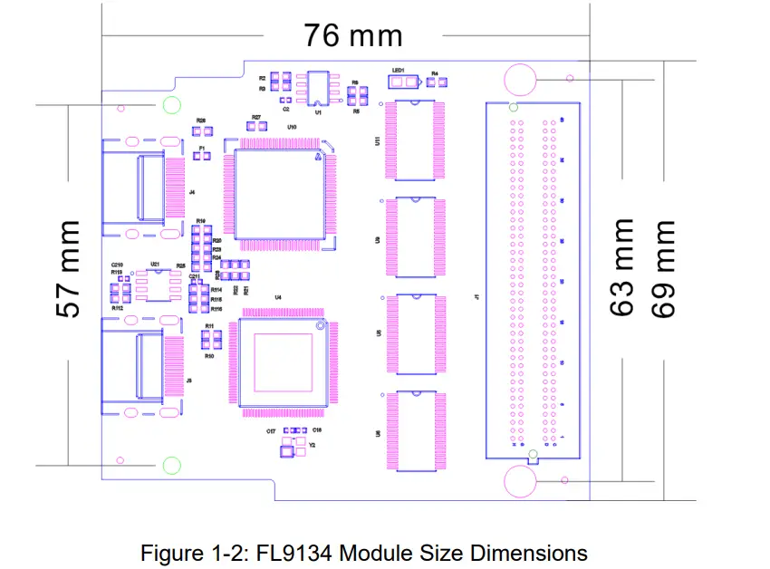
Part 1.2: FL9134 Module Size Dimension
Part 2: FL9134 Module Function Description
Part 2.1 FL9134 Module Block Diagram
Figure 2-1: FL9134 Module Block Diagram as below
Part 2.2: FL9134 Module FMC LPC pin assignment
Only the signals of the power supply and the AD chip interface are listed below, and the signal of the GND is not listed. For the detail, refer to the schematic diagram.
| Pin Number | Signal Name | Description |
| C35 | +12V | 12V Power Input |
| C37 | +12V | 12V Power Input |
| D32 | +3.3V | 3.3VPower Input |
| C34 | GAO | Bit() of EEPROM address |
| D35 | GA1 | Bit1 of EEPROM address |
| D8 | HDMI_9013_CLK | HDMI Input clock |
| G18 | HDM1_9013_D00 | HDMI Input date Bit 0 |
| D18 | HDM1_9013_D01 | HDMI Input date Bit 1 |
| H17 | HDM1_9013_D02 | HDMI Input date Bit 2 |
| G16 | HDM1_9013_D03 | HDMI Input date Bit 3 |
| H16 | HDM1_9013_D04 | HDMI Input date Bit 4 |
| G15 | HDM1_9013_DO5 | HDMI Input date Bit 5 |
| D17 | HDM1_9013_D06 | HDMI Input date Bit 6 |
| H14 | HDM1_9013_D07 | HDMI Input date Bit 7 |
| G13 | HDM1_9013_D08 | HDMI Input date Bit 8 |
| H13 | HDM1_9013_D09 | HDMI Input date Bit 9 |
| G12 | HDMI_9013_D10 | HDMI Input date Bit 10 |
| D15 | HDMI_9013_D11 | HDMI Input date Bit 11 |
| H11 | HDMI_9013_D12 | HDMI Input date Bit 12 |
| G10 | HDMI_9013_D13 | HDMI Input date Bit 13 |
| H10 | HDMI_9013_D14 | HDMI Input date Bit 14 |
| G9 | HDMI_9013_D15 | HDMI Input date Bit 15 |
| D14 | HDMI_9013_D16 | HDMI Input date Bit 16 |
| H8 | HDMI_9013_D17 | HDMI Input date Bit 17 |
| G7 | HDMI_9013_D18 | HDMI Input date Bit 18 |
| H7 | HDMI_9013_D19 | HDMI Input date Bit 19 |
| G6 | HDMI_9013_D20 | HDMI Input date Bit 20 |
| D9 | HDMI_9013_D21 | HDMI Input date Bit 22 |
| 10 | HDMI_9013_D22 | HDMI Input date Bit 22 |
| 11 | HDMI_9013_D23 | HDMI Input date Bit 23 |
| H19 | HDMI_9013_DE | HDMI input data Enable |
| G19 | HDMI_9013_HS | HDMI input image line sync |
| C23 | HDMI_9013_NRESET | 9013 chip reset signal |
| C18 | HDMI_9013_SCL | 9013 chip I2C clock |
| C19 | HDMI_9013_SDA | 9013 chip I2C data |
| H2O | HDMI_9013_VS | HDMI input image column sync |
| H32 | HDMI_9134_CLK | HDMI output clock |
| G36 | HDM1_9134_D00 | HDMI Output date Bit 0 |
| H35 | HDM1_9134_D01 | HDMI Output date Bit 1 |
| G34 | HDM1_9134_D02 | HDMI Output date Bit 2 |
| H34 | HDM1_9134_D03 | HDMI Output date Bit 3 |
| G33 | HDM1_9134_D04 | HDMI Output date Bit 4 |
| G31 | HDM1_9134_D05 | HDMI Output date Bit 5 |
| H31 | HDM1_9134_D06 | HDMI Output date Bit 6 |
| G30 | HDMI_9134_D07 | HDMI Output date Bit 7 |
| D27 | HDM1_9134_D08 | HDMI Output date Bit 8 |
| H29 | HDMI_9134_D09 | HDMI Output date Bit 9 |
| G28 | HDMI_9134_D10 | HDMI Output date Bit 10 |
| H28 | HDMI_9134_D11 | HDMI Output date Bit 11 |
| G27 | HDMI_9134_D12 | HDMI Output date Bit 12 |
| D24 | HDMI_9134_D13 | HDMI Output date Bit 13 |
| H26 | HDMI_9134_D14 | HDMI Output date Bit 14 |
| G25 | HDMI_9134_D15 | HDMI Output date Bit 15 |
| H25 | HDMI_9134_D16 | HDMI Output date Bit 16 |
| D23 | HDMI_9134_D17 | HDMI Output date Bit 17 |
| G24 | HDMI_9134_D18 | HDMI Output date Bit 18 |
| H23 | HDMI_9134_D19 | HDMI Output date Bit 18 |
| G22 | HDMI_9134_D20 | HDMI Output date Bit 20 |
| H22 | HDMI_9134_D21 | HDMI Output date Bit 21 |
| G21 | HDMI_9134_D22 | HDMI Output date Bit 22 |
| D20 | HDMI_9134_D23 | HDMI Output date Bit 23 |
| H37 | HDMI_9134_DE | HDMI Output data Enable |
| G37 | HDMI_9134_HS | HDMI Output image line sync |
| C22 | HDMI_9134_INT | 9134 chip interrupt signal |
| D26 | HDMI_9134_NRESET | 9134 chip Reset signal |
| C26 | HDMI_9134_SCL | 9134 chip 120 clock |
| C27 | HDMI_9134_SDA | 9134 chip 120 data |
| H38 | HDMI_9134_VS | HDMI output image column sync |
| D11 | HDMI_DSCL | HDMI EDID clock |
| D12 | HDMI_DSDA | HDMI EDID data |
| D21 | HPDET_EN | HOT PLUG detection signal enable |
| C30 | SCL | EEPROM 120 clock |
| C31 | SDA | EEPROM 120 data |
| G39 | VADJ | VADJ power input |
| H40 | VADJ | VADJ power input |
Part 3: HDMI DEMO program description
We provide an HDMI loop test routine for the ALINX FPGA development board, in which the video image of the HDMI input is looped directly to the HDMI output image. In addition, the register configuration and EDID information of the SiI9013 and SiI9134 chips are generated in the program.
EDID describes the display information and is an important part of the video system, indicating the format supported by the HDMI Receiver section of the HDMI module. The general EDID is the I2C interface, and the information is stored in the EEPROM. However, in this design, the EDID information is stored in the FPGA chip and implemented by the program. The external master device can access the EDID information of the HDMI module through I2C. 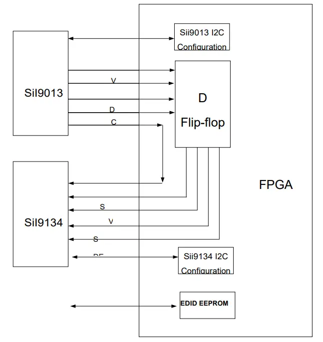
Figure 3-1: FPGA loop test
Here’s a brief introduction to the various modules used in the FPGA program:
- hdmi_loop.v
TOP program module, instantiate several sub-modules, and perform 2-level latching on the video signal of HDMI input - i2c_config.v
This module configured the register of the SiI9134 chip and SiI9013 by calling the I2C communication module. The configured register address and value are defined in the lut_data register. The specific register meanings refer to the chip manuals of SiI9134 and SiI9013. - i2c_config.v
Power-on reset module, after power-on, generates a software reset to initialize other modules - EEPROM_8b.v
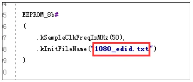
The EDID slave device of the analog EEPROM, the external display master device can read the EDID information through the I2C bus. An EEPROM register is defined in the program for storing the EDID information. The EDID information is initialized by reading the .txt file when the power is turned on. Users can modify different .EDED.txt files to achieve different video input formats. By default, we choose to support 1080P input format.
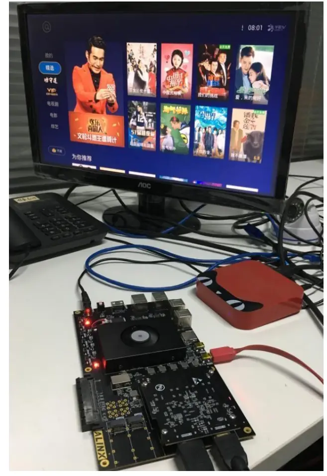
Part 4: Hardware connection and testing
The hardware connection between the FL9134 module and the FPGA development board is very simple. Simply plug the FL0214 FMC interface into the FMC interface of the FPGA development board and fix it with screws. The following is the hardware connection diagram of the ALINX AX7350 development board and FL9134 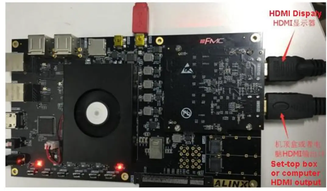
After the FPGA development board is powered on, the download program can display the computer output or the video image of the set-top box on the HDMI display (in the experiment, the HDMI input is connected to the video output of the set-top box, so the HDMI display shows the video image output by the set-top box) .