![]() R9A06G062GNP/RTK0EE0013D10001BJ
R9A06G062GNP/RTK0EE0013D10001BJ
Sub-GHz Wireless Communication Evaluation Kit For North America
User Manual
R9A06G062GNP Sub GHz Wireless Communication Evaluation Kit
All information contained in these materials, including products and product specifications, represents information on the product at the time of publication and is subject to change by Renesas Electronics Corp. without notice. Please review the latest information published by
Notice
- Descriptions of circuits, software and other related information in this document are provided only to illustrate the operation of semiconductor products and application examples. You are fully responsible for the incorporation or any other use of the circuits, software, and information in the design of your product or system. Renesas Electronics disclaims any and all liability for any losses and damages incurred by you or third parties arising from the use of these circuits, software, or information.
- Renesas Electronics hereby expressly disclaims any warranties against and liability for infringement or any other claims involving patents, copyrights, or other intellectual property rights of third parties, by or arising from the use of Renesas Electronics products or technical information described in this document, including but not limited to, the product data, drawings, charts, programs, algorithms, and application examples.
- No license, express, implied or otherwise, is granted hereby under any patents, copyrights or other intellectual property rights of Renesas Electronics or others.
- You shall be responsible for determining what licenses are required from any third parties, and obtaining such licenses for the lawful import, export, manufacture, sales, utilization, distribution or other disposal of any products incorporating Renesas Electronics products, if required.
- You shall not alter, modify, copy, or reverse engineer any Renesas Electronics product, whether in whole or in part. Renesas Electronics disclaims any and all liability for any losses or damages incurred by you or third parties arising from such alteration, modification, copying or reverse engineering.
- Renesas Electronics products are classified according to the following two quality grades: “Standard” and “High Quality”. The intended applications for each Renesas Electronics product depends on the product’s quality grade, as indicated below.
“Standard”: Computers; office equipment; communications equipment; test and measurement equipment; audio and visual equipment; home electronic appliances; machine tools; personal electronic equipment; industrial robots; etc.
“High Quality”: Transportation equipment (automobiles, trains, ships, etc.); traffic control (traffic lights); large-scale communication equipment; key financial terminal systems; safety control equipment; etc.
Unless expressly designated as a high reliability product or a product for harsh environments in a Renesas Electronics data sheet or other Renesas Electronics document, Renesas Electronics products are not intended or authorized for use in products or systems that may pose a direct threat to human life or bodily injury (artificial life support devices or systems; surgical implantation; etc.), or may cause serious property damage (space system; undersea repeaters; nuclear power control systems; aircraft control systems; key plant systems; military equipment; etc.). Renesas Electronics disclaims any and all liability for any damages or losses incurred by you or any third parties arising from the use of any Renesas Electronics product that is inconsistent with any Renesas Electronics data sheet, user’s manual or other Renesas Electronics document. - No semiconductor product is absolutely secure. Notwithstanding any security measures or features that may be implemented in Renesas Electronics hardware or software products, Renesas Electronics shall have absolutely no liability arising out of any vulnerability or security breach, including but not limited to any unauthorized access to or use of a Renesas Electronics product or a system that uses a Renesas Electronics product. RARENESS ELECTRONICS DOES NOT WARRANT OR GUARANTEE THAT RARENESS ELECTRONICS PRODUCTS, OR ANY SYSTEMS CREATED USING RARENESS ELECTRONICS PRODUCTS WILL BE INVULNERABLE OR FREE FROM CORRUPTION, ATTACK, VIRUSES, INTERFERENCE, HACKING, DATA LOSS OR THEFT, OR OTHER SECURITY INTRUSION (“Vulnerability Issues”). RARENESS ELECTRONICS DISCLAIMS ANY AND ALL RESPONSIBILITY OR LIABILITY ARISING FROM OR RELATED TO ANY VULNERABILITY ISSUES. FURTHERMORE, TO THE EXTENT PERMITTED BY APPLICABLE LAW, RARENESS ELECTRONICS DISCLAIMS ANY AND ALL WARRANTIES, EXPRESS OR IMPLIED, WITH RESPECT TO THIS DOCUMENT AND ANY RELATED OR ACCOMPANYING SOFTWARE OR HARDWARE, INCLUDING BUT NOT LIMITED TO THE IMPLIED WARRANTIES OF MERCHANTABILITY, OR FITNESS FOR A PARTICULAR PURPOSE.
- When using Renesas Electronics products, refer to the latest product information (data sheets, user’s manuals, application notes, “General Notes for Handling and Using Semiconductor Devices” in the reliability handbook, etc.), and ensure that usage conditions are within the ranges specified by Renesas Electronics with respect to maximum ratings, operating power supply voltage range, heat dissipation characteristics, installation, etc. Renesas Electronics disclaims any and all liability for any malfunctions, failure or accident arising out of the use of Renesas Electronics products outside of such specified ranges.
- Although Renesas Electronics endeavors to improve the quality and reliability of Renesas Electronics products, semiconductor products have specific characteristics, such as the occurrence of failure at a certain rate and malfunctions under certain use conditions. Unless designated as a high reliability product or a product for harsh environments in a Renesas Electronics data sheet or other Renesas Electronics document, Renesas Electronics products are not subject to radiation resistance design. You are responsible for implementing safety measures to guard against the possibility of bodily injury, injury or damage caused by fire, and/or danger to the public in the event of a failure or malfunction of Renesas Electronics products, such as safety design for hardware and software, including but not limited to redundancy, fire control and malfunction prevention, appropriate treatment for aging degradation or any other appropriate measures. Because the evaluation of microcomputer software alone is very difficult and impractical, you are responsible for evaluating the safety of the final products or systems manufactured by you.
- Please contact a Renesas Electronics sales office for details as to environmental matters such as the environmental compatibility of each Renesas Electronics product. You are responsible for carefully and sufficiently investigating applicable laws and regulations that regulate the inclusion or use of controlled substances, including without limitation, the EU RoHS Directive, and using Renesas Electronics products in compliance with all these applicable laws and regulations. Renesas Electronics disclaims any and all liability for damages or losses occurring as a result of your noncompliance with applicable laws and regulations.
- Renesas Electronics products and technologies shall not be used for or incorporated into any products or systems whose manufacture, use, or sale is prohibited under any applicable domestic or foreign laws or regulations. You shall comply with any applicable export control laws and regulations promulgated and administered by the governments of any countries asserting jurisdiction over the parties or transactions.
- It is the responsibility of the buyer or distributor of Renesas Electronics products, or any other party who distributes, disposes of, or otherwise sells or transfers the product to a third party, to notify such third party in advance of the contents and conditions set forth in this document.
- This document shall not be reprinted, reproduced or duplicated in any form, in whole or in part, without prior written consent of Renesas Electronics.
- Please contact a Renesas Electronics sales office if you have any questions regarding the information contained in this document or Renesas Electronics products.
(Note 1) “Renesas Electronics” as used in this document means Renesas Electronics Corporation and also includes its directly or indirectly controlled subsidiaries.
(Note 2) “Renesas Electronics product(s)” means any product developed or manufactured by or for Renesas Electronics.
(Rev.5.0-1 October 2020)
Corporate Headquarters
TOYOSU FORESIA, 3-2-24 Toyosu,
Koto-ku, Tokyo 135-0061, Japan
www.renesas.com
Trademarks
Renesas and the Renesas logo are trademarks of Renesas
Electronics Corporation. All trademarks and registered trademarks are the property of their respective owners.
Contact information
For further information on a product, technology, the most up-to-date version of a document, or your nearest sales office, please visit: www.renesas.com/contact/.
General Precautions in the Handling of Micro processing Unit and Micro controller Unit Products
The following usage notes are applicable to all Micro processing unit and Micro controller unit products from Renesas. For detailed usage notes on the products covered by this document, refer to the relevant sections of the document as well as any technical updates that have been issued for the products.
- Precaution against Electrostatic Discharge (ESD)
A strong electrical field, when exposed to a CMOS device, can cause destruction of the gate oxide and ultimately degrade the device operation. Steps must be taken to stop the generation of static electricity as much as possible, and quickly dissipate it when it occurs. Environmental control must be adequate. When it is dry, a humidifier should be used. This is recommended to avoid using insulators that can easily build up static electricity. Semiconductor devices must be stored and transported in an anti-static container, static shielding bag or conductive material. All test and measurement tools including work benches and floors must be grounded. The operator must also be grounded using a wrist strap. Semiconductor devices must not be touched with bare hands. Similar precautions must be taken for printed circuit boards with mounted semiconductor devices. - Processing at power-on
The state of the product is undefined at the time when power is supplied. The states of internal circuits in the LSI are indeterminate and the states of register settings and pins are undefined at the time when power is supplied. In a finished product where the reset signal is applied to the external reset pin, the states of pins are not guaranteed from the time when power is supplied until the reset process is completed. In a similar way, the states of pins in a product that is reset by an on-chip power-on reset function are not guaranteed from the time when power is supplied until the power reaches the level at which resetting is specified. - Input of signal during power-off state
Do not input signals or an I/O pull-up power supply while the device is powered off. The current injection that results from input of such a signal or I/O pull-up power supply may cause malfunction and the abnormal current that passes in the device at this time may cause degradation of internal elements. Follow the guideline for input signal during power-off state as described in your product documentation. - Handling of unused pins
Handle unused pins in accordance with the directions given under handling of unused pins in the manual. The input pins of CMOS products are generally in the high-impedance state. In operation with an unused pin in the open-circuit state, extra electromagnetic noise is induced in the vicinity of the LSI, an associated shoot-through current flows internally, and malfunctions occur due to the false recognition of the pin state as an input signal become possible. - Clock signals
After applying a reset, only release the reset line after the operating clock signal becomes stable. When switching the clock signal during program execution, wait until the target clock signal is stabilized. When the clock signal is generated with an external resonator or from an external oscillator during a reset, ensure that the reset line is only released after full stabilization of the clock signal. Additionally, when switching to a clock signal produced with an external resonator or by an external oscillator while program execution is in progress, wait until the target clock signal is stable. - Voltage application waveform at input pin
Waveform distortion due to input noise or a reflected wave may cause malfunction. If the input of the CMOS device stays in the area between VIL (Max.) and VIH (Min.) due to noise, for example, the device may malfunction. Take care to prevent chattering noise from entering the device when the input level is fixed, and also in the transition period when the input level passes through the area between VIL (Max.) and VIH (Min.). - Prohibition of access to reserved addresses
Access to reserved addresses is prohibited. The reserved addresses are provided for possible future expansion of functions. Do not access these addresses as the correct operation of the LSI is not guaranteed. - Differences between products
Before changing from one product to another, for example to a product with a different part number, confirm that the change will not lead to problems. The characteristics of a micro processing unit or microcontroller unit products in the same group but having a different part number might differ in terms of internal memory capacity, layout pattern, and other factors, which can affect the ranges of electrical characteristics, such as characteristic values, operating margins, immunity to noise, and amount of radiated noise. When changing to a product with a different part number, implement a system evaluation test for the given product.
How to Use This Manual
- Purpose and Target Readers
This manual is intended to give users an understanding of the basic specifications and correct usage of this product. This manual is intended for users who want to use this product to evaluate the MCU and debug programs. The readers of this manual are expected to have knowledge of the MCU functions and debuggers.
Particular attention should be paid to the precautionary notes when using the manual. These notes occur within the body of the text, at the end of each section, and in the Usage Notes section.
The revision history summarizes the locations of revisions and additions. It does not list all revisions. Refer to the text of the manual for details.
The following documents apply to RTK0EE0013D10001BJ. Be sure to refer to the latest versions of these documents.
The newest versions of the listed documents are available on the Renesas Electronics Web site.Document Type Description Document Title Document No. User’s manual RTK0EE0013D10001BJ
hardware specificationsRTK0EE0013D10001BJ
User’s ManualR02UZ0004EJ (this manual) Design data RTK0EE0013D10001BJ
Circuit schematics
Parts listRTK0EE0013D10001BJ
Circuit schematics
Parts listR02AN0047EJ User’s manual for R9A06G062GNP Hardware specifications (pin assignments, peripheral function specifications, electrical characteristics, timing charts) and descriptions of operation R9A06G062GNP
Sub-GHz Transceiver User’s Manual: HardwareR02UH0006EJ RX65N
User’s manual for the hardwareHardware specifications (pin assignments, memory maps, peripheral function specifications, electrical characteristics, timing charts) and descriptions of operation RX65N Group User’s Manual: Hardware R01UH0590EJ ISL80510 Datasheet Hardware specifications (pin assignments, electrical characteristics) and descriptions of operation ISL80510 Datasheet FN8767 ISL9005A Datasheet Hardware specifications (pin assignments, electrical characteristics) and descriptions of operation ISL9005A Datasheet FN6452
Overview
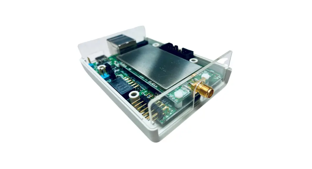
1. 1 Package Components
Thank you for purchasing the Sub-GHz Wireless Communication Evaluation Kit from Renesas (hereinafter referred to as “this product”). This product consists of the Target Board for Sub-GHz Wireless Communication Evaluation Kit (RTK0EE0013D10001BJ)
1.2 Purpose
This product is an evaluation tool for a Sub-GHz Wireless Communication Solutions. This manual descries hardware specifications.
1.3 Features
This product includes the following features:
- Sub-GHz Wireless Communication evaluation
This product offers sub-GHz wireless communication solutions with FCC of North America to help you easily start developing your application.
1.4 Sub-GHz Wireless Communication Evaluation Kit: Table of Specifications
Table 1-1 shows the specifications of this product.
Table 1-1: Sub-GHz Wireless Communication Evaluation Kit Specification Table
| Item | Specification |
| Enclosure size | Size: 92.0 mm x 66.5 mm x 28.0 mm |
| Operating ambient temperature | -10 to +60°C |
| Power-supply circuit | USB connector: 5-V input |
| Transceiver IC (CWX-M) | Part Number: R9A06G062GNP (Renesas) |
| Package: 40-Pin HVQFN | |
| Control MCU (RX65N) | Part Number: R5F565NEDDFP (Renesas) |
| Package: 100pin LFQFP | |
| Power-supply IC | Part Number: ISL80510 (Renesas) |
| Part Number: ISL9005A (Renesas) | |
| SAW filter | Part Number: B39921B2672P810 (Qualcomm) |
| FEM | Part Number: SKY66122-11(Skyworks) |
| Control MCU/ Main clock | Connected to CKOUT pin of CWX-M (16MHz) |
| Control MCU/ Sub-clock | Crystal oscillator for the sub-clock (32.768 KHz) |
| Wireless function | Sub-GHz Wireless circuit |
| North America Band: 902 to 928MHz (FCC) | |
| Modulation Method: FSK / OFDM | |
| USB:Type-C USB bus power (DC5.0V/3.0A) USB2.0 | Connector for an on-board emulator: |
| USB Connector for a USB serial-conversion interface | |
| Setting of USB Mode | DIP switch x1 |
| Ethernet | Part Number: LAN8720A (Microchip) Note: The Ethernet function is disabled on this product. |
| Antenna | Part Number: TI.92.2113 (Taoglas limited) |
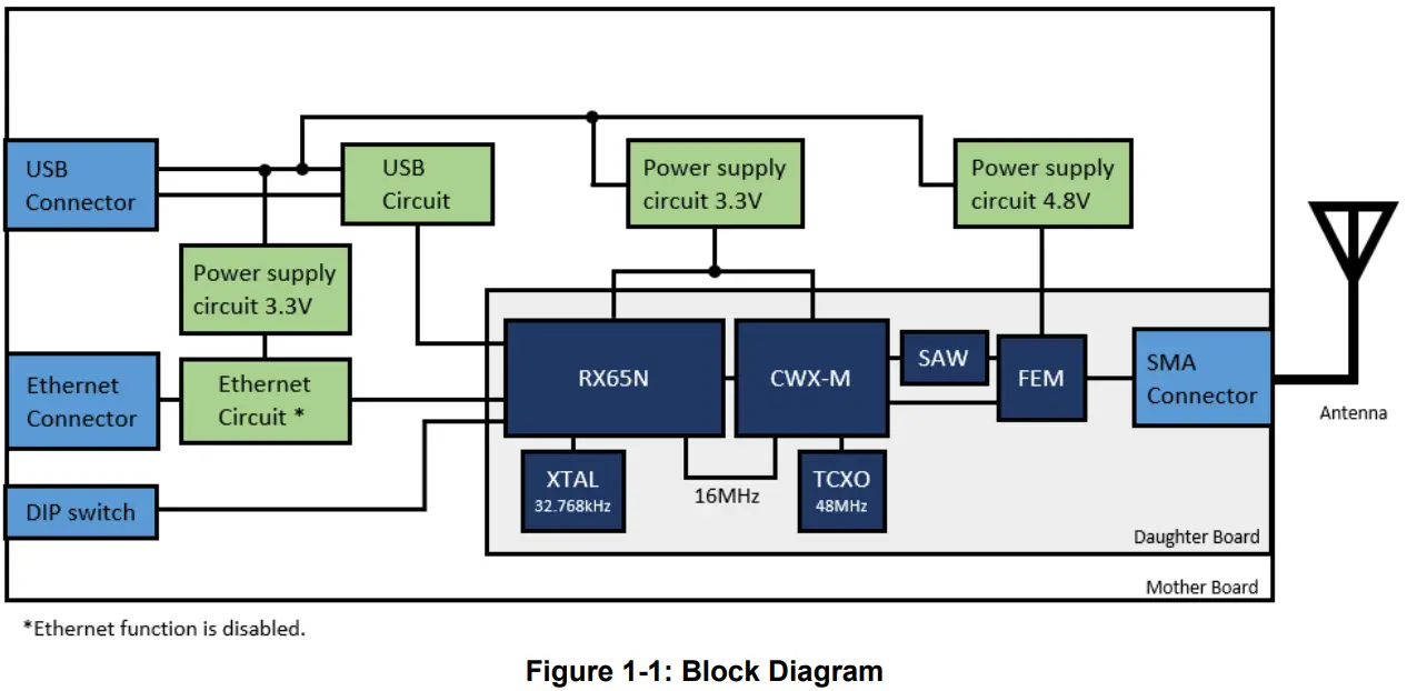
1.5 Block Diagram
Figure 1-1 shows the block diagram of this product.
External view
Figure 2-1 shows the external view of this product.
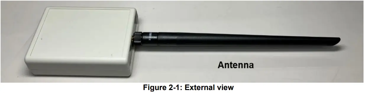
This product includes Sub-GHz wireless function.
The antenna of this product permanently glued with epoxy to the SMA connector and cannot be removed.
Note:
Never disassemble or remodel this product.
Never use an antenna other than the antenna provided with the product, as it violates the radio-related laws.
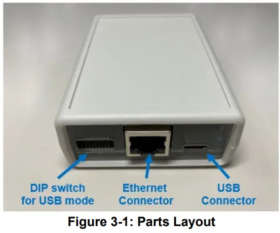
Parts Layout
Figure 3-1 shows the parts layout of this product.
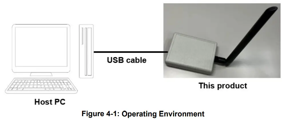
Operating Environment
Figure 4-1 shows the operating environment of this product. Install “Virtual COM Port USB Driver” on the host PC. In addition, install the serial terminal software as it will be used for wireless evaluation.
4.1 Virtual COM Port USB Driver
If your PC is connected to the Internet, Windows Update will automatically install the latest driver. Please wait until you see the following pop-up message: Your device is ready to use. If you have not yet installed the driver on your PC, Download and install the driver. Virtual COM port drivers can be downloaded from the FTDI website. FTDI manufactures USB chips embedded in this product.
FTDI website: http://www.ftdichip.com/Drivers/VCP.htm
4.2 Serial Terminal Software
The serial terminal software enables data to be input to and output from a serial console.
The serial terminal settings are as shown in Table 4-1.
Table 4-1: Serial Terminal Settings
| Setting item | Setting value |
| Baud rate | 500000 bps |
| Data | 8 bits |
| Parity | None |
| Stop bit | 1 bit |
| Flow control | Not used |
| Newline code | Reception: LF or AUTO Transmission: CR+LF or LF |
| Local echo | Enabled |
Note:
Windows does not come with serial terminal software. Please use the free terminal software of your choice.
User Circuits
5.1 DIP switch
Set the following when evaluating (normal mode).
Table 5-1: DIP switch Settings
| Mode | DIP switch Settings |
| Evaluation (normal mode) | 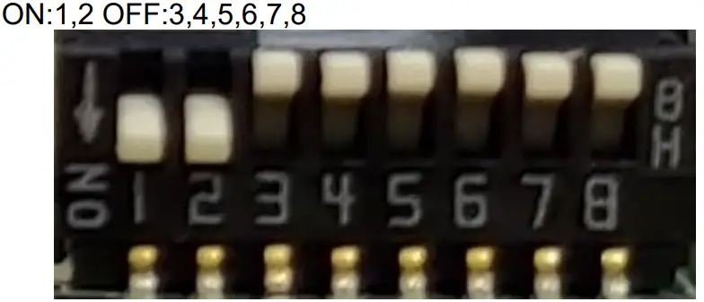 |
5.2 Connection of control MCU(RX65N) and wireless transceiver IC (CWX-M)
Table 5-2: Connection of control MCU(RX65N) and wireless transceiver IC (CWX-M)
| Control MCU(RX65N) | Transceiver IC (CWX-M) | Note |
| RSTB | P46 | CWX-M reset control |
| MODE | P47 | CWX-M operation mode control |
| INTOUT0 | PD5 | CWX-M GPIO0 |
| INTOUT1 | PD6 | CWX-M GPIO1 *1 |
| INTOUT2 | PD7 | CWX-M GPIO2 *1 |
| CLK | PD3 | SPI Serial clock *2 |
| SEN | PD4 | SPI Slave select *2 |
| SIN | PD1 | SPI MOSI(Master Out Slave In) *2 |
| SOUT | PD2 | SPI MISO(Master In Slave Out) *2 |
*1 Reserved for option use.
*2 RX65N is master device.
Wireless evaluation
6.1 Serial terminal software connection settings
- Connect the host PC and this product with a USB cable.
- Check which COM port the USB of this product is assigned to using the device manager.
- Start up the serial terminal software and set serial port.
6.2 Command specification
- When the sample program is started, it enters “command menu mode” and is ready to accept commands.Table 6-1 shows the command list of sample program.
- To execute the function of a command, enter the command and then press the return key. When the command has an argument, enter the command, a space and the argument, and then press the return key.
Table 6-1: Command list of sample program
| Command | Function | Argument |
| tboot | Renesas Sub-GHz transceiver bootstrapping | Boot mode |
| tinit | Test function initialization and reset Renesas Sub-GHz transceiver | (None) |
| tope | PHY operation mode setting | FSK/OFDM operation mode Prohibit the use in modes other than the following. tope FSK NA FSKwoFEC 1b 1 tope FSK NA FSKwoFEC 3 2 tope OFDM NA OFDMOP4 MCS6 1 tope OFDM NA OFDMOP3 MCS6 2 tope OFDM NA OFDMOP2 MCS6 4 tope OFDM NA OFDMOP1 MCS6 5 |
| tch | Channel number setting | Channel number |
| ttxpow | FSK and OFDM transmission output power setting | Transmission output power value (Index number) |
| ttxpowd | FSK and OFDM transmission output power setting (dBm) | Transmission output power value (dBm) |
| tftxpowd | FSK transmission output power setting (dBm) | FSK transmission output power value (dBm) |
| totxpowd | OFDM transmission output power setting (dBm) | OFDM transmission output power value (dBm) |
| trxgain | External gain setting for reception signal | External gain value for RF input signal |
| trxgaind | External gain setting for reception signal | External gain value for RF input signal(dBm) |
| tfrlen | Transmission packet length setting | Transmission packet length |
| ti | Continuous transmission interval time setting | Continuous transmission interval time setting |
| ttxopt | Transmission option setting | Transmission option |
| tsfd | FSK SFD mode setting | FSK SFD mode |
| tfpl | FSK Preamble length setting | FSK Preamble length |
| tdw | FSK Data whitening option setting | FSK Data whitening option |
| tffcs | FSK FCS length setting | FSK FCS length |
| tfscheme | FSK FEC scheme setting | FSK FEC Scheme |
| tffecrx | FSK Reception packet FEC setting | FSK FEC setting |
| tofcs | OFDM FCS length setting | FSK FCS length (CRC bit width) |
| tointl | OFDM Interleaving mode setting | Interleaving mode |
| toscr | OFDM Scrambler value setting | OFDM Scrambler value |
| tostf | OFDM STF length setting | OFDM STF length |
| tccam | CCA mode setting | CCA mode |
| tfcdr | CCA duration setting for FSK | CCA duration for FSK |
| tfccavt | CCA level threshold for FSK | CCA level threshold value for FSK |
| tfccavtd | CCA level threshold for FSK in dBm | CCA level threshold value (dBm) for FSK |
| tocdr | CCA duration setting for OFDM | CCA duration for OFDM |
| toccavt | CCA level threshold for OFDM | CCA level threshold value for OFDM |
| toccavtd | CCA level threshold for OFDM in dBm | CCA level threshold value (dBm) for OFDM |
| tgpios | GPIO terminal setting | GPIO terminal function |
| tgpio | Get the current settings of the GPIO terminal | (None) |
| tgpioo | GPIO output port voltage level setting | GPIO output port voltage level |
| tgpioi | Get the GPIO input port voltage level | GPIO port number |
| tberlen | Frame length for RX BER setting | Frame length for RX BER |
| tberpn9 | PN9 mode for BER setting | PN9 mode for BER |
| tffh | Frequency hopping transmission (FSK) | Setting for frequency hopping transmission |
| tofh | Frequency hopping transmission (OFDM) | Setting for frequency hopping transmission |
| ram | RAM read and write mode | read and write mode setting |
| reg | Register read and write mode | read and write mode setting |
| tftx | FSK Packet transmission | Number of transmissions |
| totx | OFDM Packet transmission | Number of transmissions |
| tfpn9 | FSK PN9 continuous modulated transmission | (None) |
| topn9 | OFDM PN9 continuous modulated transmission | (None) |
| tnmtx | Continuous unmodulated transmission | (None) |
| tfrx | FSK Packet reception | Reception option |
| torx | OFDM Packet reception | Reception option |
| te | ED measurement | (None) |
| tcca | CCA execution | (None) |
| tmstxs | Tx setting for Mode Switch & New Mode Frame | Setting option |
| tmstx | Mode Switch & New Mode Frame transmission | Number of transmissions |
| tmsrxs | Rx setting for Mode Switch & New Mode Frame | Setting option |
| tmsrx | Mode Switch & New Mode Frame reception | Reception options |
| tttl | Regulation mode setting (Tx Total Time Limit, Max Tx Duration and Min Pause Duration Setting) | Regulation mode and parameters |
| tantdv | Antenna diversity setting | Enable / Disable |
| tantnum | Setting the number of antennas to use | Number of antennas |
| tantsel | Setting the antenna number used for Tx / Rx | Antenna number |
| rst | Reset all (Test function, RF driver and Renesas Sub-GHz transceiver) | (None) |
| opt | Test function option setting | Display mode of Test function |
| val | Test function settings display | (None) |
| help | Command list display | (None) |
| tsleep | Sleep Mode Setting | (None) |
- The gray areas are commands not supported by this product.
- The transmission output power setting of R9A06G062GNP is fixed to the following settings. It cannot be changed by command.
FSK: 1.5 dBm OFDM: -2.0 dBm - Details on the command specification is explained in the application note ” RF Characteristic Evaluation Program for Renesas Sub-GHz Transceiver Operation Manual (R30AN0376)”. Obtain the latest version of this document from the Renesas website.
Hardware specifications
Table 7-1 shows the communication specifications of this product.
Table 7-1: Communication specifications
| Channel Spacing | Modulation | ||||
| Option | MCS | Data Rate/Modulation Index | |||
| North America Band 902 – 928 MHz | OFDM | 1200 KHz | Option 1 | MCS 6 | 2400 kbps |
| 800 KHz | Option 2 | MCS 6 | 1200 kbps | ||
| 400 KHz | Option 3 | MCS 6 | 600 kbps | ||
| 200KHz | Option 4 | MCS 6 | 300 kbps | ||
| FSK | 200KHz | Operating mode #1b | 50 kbps / m=1.0 | ||
| 400 KHz | Operating mode #3 | 150 kbps / m=0.5 | |||
7.1 North America Band
7.1.1 OFDM, Channel Spacing = 1200 KHz, Modulation = Option 1/MCS 6/2400 kbps
- Transmission output power at SMA connecter = +24 dBm
- Channel Number Setting: Chan Plan ID 5
Channel number Frequency [MH z] Channel number Frequency [MHz] Channel number Frequency [MHz] Channel number Frequency [MHz] 0 903.2 1 904.4 2 905.6 3 906.8 4 908.0 5 909.2 6 910.4 7 911.6 8 912.8 9 914.0 10 915.2 11 916.4 12 917.6 13 918.8 14 920.0 15 921.2 16 922.4 17 923.6 18 924.8 19 926.0 20 927.2
7.1.2 OFDM, Channel Spacing = 800 KHz, Modulation = Option 2/MCS 6/1200 kbps
- Transmission output power at SMA connecter = +24 dBm
- Channel Number Setting: Chan Plan ID 4
Channel number Frequency [MH z] Channel number Frequency [MHz] Channel number Frequency [MHz] Channel number Frequency [MHz] 0 902.8 1 903.6 2 904.4 3 905.2 4 906.0 5 906.8 6 907.6 7 908.4 8 909.2 9 910.0 10 910.8 11 911.6 12 912.4 13 913.2 14 914.0 15 914.8 16 915.6 17 916.4 18 917.2 19 918.0 20 918.8 21 919.6 22 920.4 23 921.2 24 922.0 25 922.8 26 923.6 27 924.4 28 925.2 29 926.0 30 926.8 31 927.6
7.1.3 OFDM, Channel Spacing = 400 KHz, Modulation = Option 3/MCS 6/600 kbps
- Transmission output power at SMA connecter = +24 dBm
- Channel Number Setting: Chan Plan ID 2
Channel number Frequency [MH z] Channel number Frequency [MHz] Channel number Frequency [MHz] Channel number Frequency [MHz] 0 902.4 1 902.8 2 903.2 3 903.6 4 904.0 5 904.4 6 904.8 7 905.2 8 905.6 9 906.0 10 906.4 11 906.8 12 907.2 13 907.6 14 908.0 15 908.4 16 908.8 17 909.2 18 909.6 19 910.0 20 910.4 21 910.8 22 911.2 23 911.6 24 912.0 25 912.4 26 912.8 27 913.2 28 913.6 29 914.0 30 914.4 31 914.8 32 915.2 33 915.6 34 916.0 35 916.4 36 916.8 37 917.2 38 917.6 39 918.0 40 918.4 41 918.8 42 919.2 43 919.6 44 920.0 45 920.4 46 920.8 47 921.2 48 921.6 49 922.0 50 922.4 51 922.8 52 923.2 53 923.6 54 924.0 55 924.4 56 924.8 57 925.2 58 925.6 59 926.0 60 926.4 61 926.8 62 927.2 63 927.6
7.1.4 OFDM, Channel Spacing = 200KHz, Modulation = Option 4/MCS 6/300 kbps
- Transmission output power at SMA connecter = +24 dBm
- Channel Number Setting: Chan Plan ID 1
Channel number Frequency [MH z] Channel number Frequency [MHz] Channel number Frequency [MHz] Channel number Frequency [MHz] 0 902.2 1 902.4 2 902.6 3 902.8 4 903.0 5 903.2 6 903.4 7 903.6 8 903.8 9 904.0 10 904.2 11 904.4 12 904.6 13 904.8 14 905.0 15 905.2 16 905.4 17 905.6 18 905.8 19 906.0 20 906.2 21 906.4 22 906.6 23 906.8 24 907.0 25 907.2 26 907.4 27 907.6 28 907.8 29 908.0 30 908.2 31 908.4 32 908.6 33 908.8 34 909.0 35 909.2 36 909.4 37 909.6 38 909.8 39 910.0 40 910.2 41 910.4 42 910.6 43 910.8 44 911.0 45 911.2 46 911.4 47 911.6 48 911.8 49 912.0 50 912.2 51 912.4 52 912.6 53 912.8 54 913.0 55 913.2 56 913.4 57 913.6 58 913.8 59 914.0 60 914.2 61 914.4 62 914.6 63 914.8 64 915.0 65 915.2 66 915.4 67 915.6 68 915.8 69 916.0 70 916.2 71 916.4 72 916.6 73 916.8 74 917.0 75 917.2 76 917.4 77 917.6 78 917.8 79 918.0 80 918.2 81 918.4 82 918.6 83 918.8 84 919.0 85 919.2 86 919.4 87 919.6 88 919.8 89 920.0 90 920.2 91 920.4 92 920.6 93 920.8 94 921.0 95 921.2 96 921.4 97 921.6 98 921.8 99 922.0 100 922.2 101 922.4 102 922.6 103 922.8 104 923.0 105 923.2 106 923.4 107 923.6 108 923.8 109 924.0 110 924.2 111 924.4 112 924.6 113 924.8 114 925.0 115 925.2 116 925.4 117 925.6 118 925.8 119 926.0 120 926.2 121 926.4 122 926.6 123 926.8 124 927.0 125 927.2 126 927.4 127 927.6 128 927.8
7.1.5 FSK, Channel Spacing = 200KHz, 50 kbps/m = 1.0
- Transmission output power at SMA connecter = +30 dBm
- Channel Number Setting: Chan Plan ID 1
Channel number Frequency [MH z] Channel number Frequency [MHz] Channel number Frequency [MHz] Channel number Frequency [MHz] 0 902.2 1 902.4 2 902.6 3 902.8 4 903.0 5 903.2 6 903.4 7 903.6 8 903.8 9 904.0 10 904.2 11 904.4 12 904.6 13 904.8 14 905.0 15 905.2 16 905.4 17 905.6 18 905.8 19 906.0 20 906.2 21 906.4 22 906.6 23 906.8 24 907.0 25 907.2 26 907.4 27 907.6 28 907.8 29 908.0 30 908.2 31 908.4 32 908.6 33 908.8 34 909.0 35 909.2 36 909.4 37 909.6 38 909.8 39 910.0 40 910.2 41 910.4 42 910.6 43 910.8 44 911.0 45 911.2 46 911.4 47 911.6 48 911.8 49 912.0 50 912.2 51 912.4 52 912.6 53 912.8 54 913.0 55 913.2 56 913.4 57 913.6 58 913.8 59 914.0 60 914.2 61 914.4 62 914.6 63 914.8 64 915.0 65 915.2 66 915.4 67 915.6 68 915.8 69 916.0 70 916.2 71 916.4 72 916.6 73 916.8 74 917.0 75 917.2 76 917.4 77 917.6 78 917.8 79 918.0 80 918.2 81 918.4 82 918.6 83 918.8 84 919.0 85 919.2 86 919.4 87 919.6 88 919.8 89 920.0 90 920.2 91 920.4 92 920.6 93 920.8 94 921.0 95 921.2 96 921.4 97 921.6 98 921.8 99 922.0 100 922.2 101 922.4 102 922.6 103 922.8 104 923.0 105 923.2 106 923.4 107 923.6 108 923.8 109 924.0 110 924.2 111 924.4 112 924.6 113 924.8 114 925.0 115 925.2 116 925.4 117 925.6 118 925.8 119 926.0 120 926.2 121 926.4 122 926.6 123 926.8 124 927.0 125 927.2 126 927.4 127 927.6 128 927.8
7.1.6 FSK, Channel Spacing = 400 KHz, 150 kbps/m = 0.5
- Transmission output power at SMA connecter = +30 dBm
- Channel Number Setting: Chan Plan ID 2
Channel number Frequency [MH z] Channel number Frequency [MHz] Channel number Frequency [MHz] Channel
numberFrequency [MHz] 0 902.4 1 902.8 2 903.2 3 903.6 4 904.0 5 904.4 6 904.8 7 905.2 8 905.6 9 906.0 10 906.4 11 906.8 12 907.2 13 907.6 14 908.0 15 908.4 16 908.8 17 909.2 18 909.6 19 910.0 20 910.4 21 910.8 22 911.2 23 911.6 24 912.0 25 912.4 26 912.8 27 913.2 28 913.6 29 914.0 30 914.4 31 914.8 32 915.2 33 915.6 34 916.0 35 916.4 36 916.8 37 917.2 38 917.6 39 918.0 40 918.4 41 918.8 42 919.2 43 919.6 44 920.0 45 920.4 46 920.8 47 921.2 48 921.6 49 922.0 50 922.4 51 922.8 52 923.2 53 923.6 54 924.0 55 924.4 56 924.8 57 925.2 58 925.6 59 926.0 60 926.4 61 926.8 62 927.2 63 927.6
Additional Information
Technical Support
For details on the Transceiver IC (CWX-M), refer to the R9A06G062GNP Sub-GHz Transceiver User’s Manual: Hardware.
The latest information is available from the Web page.
Technical Contact Details
General information on Renesas micro controllers can be found on the Renesas website at: https://www.renesas.com/
Note
- Do not install this product into your product.
- When using this product, be sure to use the antenna provided with the product.
- Never disassemble or modify this product.
- Do not use any firmware other than the dedicated firmware for this product during wireless evaluation.
Trademarks
All brand or product names used in this manual are trademarks or registered trademarks of their respective companies or organisations.
Copyright
This document may be, wholly or partially, subject to change without notice. All rights reserved. Duplication of this document, either in whole or part is prohibited without the written permission of Renesas Electronics Corporation.
© 2022 Renesas Electronics Corporation. All rights reserved.
Certification of Compliance
This product complies with the laws and regulations described below.
9.1 Radio-Related Laws
North America: FCC ID: 2AEMXCWXMRTK1BJ
FCC Regulatory
This device complies with part 15 of the FCC Rules. Operation is subject to the following two conditions:
- This device may not cause harmful interference, and
- This device must accept any interference received, including interference that may cause undesired operation.
FCC CAUTION
Changes or modifications not expressly approved by the party responsible for compliance could void the user’s authority to operate the equipment.
This transmitter must not be co-located or operated in conjunction with any other antenna or transmitter.
This equipment complies with FCC radiation exposure limits set forth for an uncontrolled environment and meets the FCC radio frequency (RF) Exposure Guidelines. This equipment has very low levels of RF energy that it deemed to comply without maximum permissive exposure evaluation (MPE). But it is desirable that it should be installed and operated keeping the radiator at least 20cm or more away from person’s body.
This equipment has been tested and meets the FCC RF exposure guidelines when used with the Renesas accessories supplied or designated for this product. Use of other accessories may not ensure compliance with FCC RF exposure guidelines.
This equipment must be used with the approved antenna included in the product.
The certified antenna include:
TERMINAL DIPOLE ANTENNA (Taoglas: TI.92.2113) with peak gain 2.14 dBi.
The antenna of this product permanently glued with epoxy to the SMA connector and cannot be removed.
| Revision History | RTK0EE0013D10001BJ User’s Manual |
| Rev. | Date | Description | |
| Page | Summary | ||
| 1.00 | 2022.12.31 | - | First Edition issued |
![]() Renesas Electronics Corporation
Renesas Electronics Corporation
www.renesas.com
R02UZ0004EJ0100
R9A06G062GNP
RTK0EE0013D10001BJ User’s Manual
Publication Date: Rev.1.00 Dec.31.22
Published by: Renesas Electronics Corporation
Rev.1.00 2022.12
© 2022 Renesas Electronics Corporation. All rights reserved.


