onsemi XGS X-Celerator Developer Kit
INTRODUCTION
The X−Celerator kit is designed to enable FPGA development around ON Semiconductor’s XGS image sensor family. The kit provides a sensor HiSpi receiver example as starting point to allow for a quicker and more easy integration to standard FPGA evaluation environments. The interface example was created for a Xilinx UltraScale architecture.
The headboard can feature ON Semiconductor XGS 5000, XGS 12000 or XGS 16000 image sensor integrated on a standard High−Speed Array VITA 57.1 FPGA Mezzanine Card (FMC) with onboard power management.
IP CORE ARCHITECTURE
Reference RTL code for the HiSpi receiver (see Figure 2) is available under NDA and structured as three modular IP core blocks (deserializer, decoder and remapper) that convert the XGS HiSpi output to an AXI4 video streaming standard. These blocks are written in a flexible and generic form that is easily modified and inserted in any FPGA vendor technology or design methodology. The X−Celerator contains a ready-to-use block diagram example solution for each of the sensor variants, designed for the Xilinx Kintex UltraScale architecture.
Although the RTL IP core blocks have been validated to work on Altera (Intel) development boards, active support for the HiSpi receiver on these systems is currently not yet available.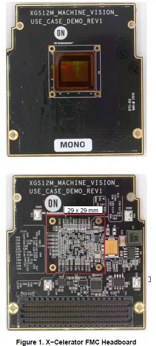
SYSTEM OVERVIEW
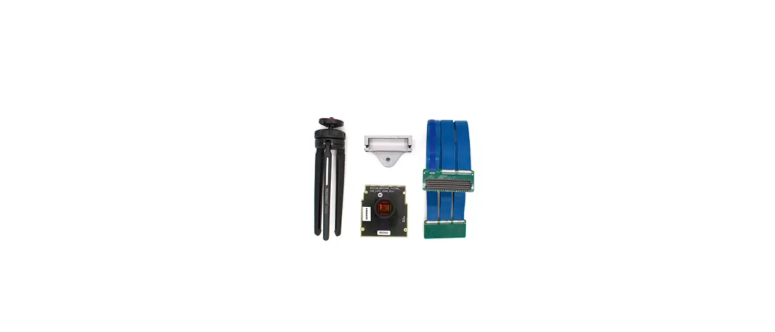
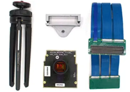
Figure 1 shows the stripped XGS 12000 X−Celerator FMC headboard (78.8 x 69 mm) with protective foil on the sensor, designed with a small form factor in mind (29 x 29 mm). This is the single part that changes between the different Orderable Part Numbers (OPN’s), provided in Table 1. The kit furthermore consists out of a lens mount, extension barrel, Low−pin Count (LPC) FMC cable, tripod mount and a tripod in order to enable a more user−friendly tripod configuration. The individual parts are discussed in more detail in the following subsections. Please note that these OPN’s do NOT include a lens or development board. 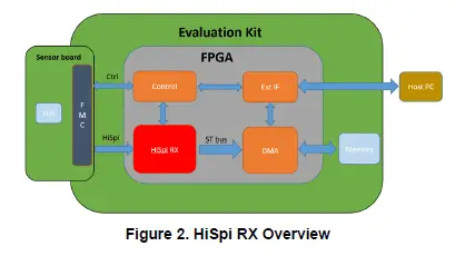
Table 1. ORDERABLE PART NUMBERS
| Part Number | Product Description |
| XCEL-NOIX4SE5000BL-GEVK | X−Celerator − XGS 5000 − color image sensor board, includes LPC FMC cable, lens mount, tri- pod mount and tripod. |
| XCEL-NOIX4SN5000BL-GEVK | X−Celerator − XGS 5000 − monochrome image sensor board, includes LPC FMC cable, lens mount, tripod mount and tripod. |
| XCEL-NOIX1SE012KBL-GEVK | X−Celerator − XGS 12000 − color image sensor board, includes LPC FMC cable, lens mount, tripod mount and tripod. |
| XCEL-NOIX1SN012KBL-GEVK | X−Celerator − XGS 12000 − monochrome image sensor board, includes LPC FMC cable, lens mount, tripod mount and tripod. |
| XCEL-NOIX1SE016KBL-GEVK | X−Celerator − XGS 16000 − color image sensor board, includes LPC FMC cable, lens mount, tripod mount and tripod. |
| XCEL-NOIX1SN016KBL-GEVK | X−Celerator − XGS 16000 − monochrome image sensor board, includes LPC FMC cable, lens mount, tripod mount and tripod. |
Image Sensor Board
This board features one of ON Semiconductor XGS image sensors implemented on an ANSI/VITA 57.1 single-width FMC standard module board with full channel (24 lanes for XGS 12000 and XGS 16000 and 16 lanes for XGS 5000) HiSpi video output, the necessary sensor control signals provided over SPI and a single 3.3 V power supply input. The ON Semiconductor’s NCP6914 Mini−PMIC provides all the necessary low-noise power supplies for image sensor operations.
Figure 3 and Table 2 show the board layout and the Bill of Materials (BOM) for the X−Celebrator. Detailed layout files and schematics are available under NDA. 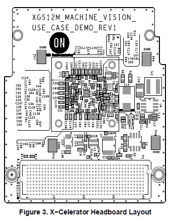
Low−pin Count (LPC) FMC Cable
Provided with the OPN’s comes a VITA 57.1 FMC Samtec LPC HDR Cable, as shown in Figure 4, to connect the headboard in its tripod configuration. Specifications on the usable cables can be found on the Samtec VITA family webpage.
The provided cable (HDR−169473−01) is the LPC variant of the FMC connection, chosen for improved flexibility, proof of concept and reduced costs. The HPC variant of this cable can be chosen just as well but is not provided in this development kit OPN.
More information on LPC vs HPC can be found in the section on FMC connection pins. 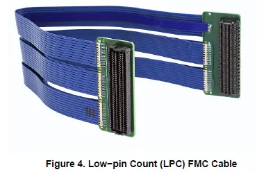
DIMENTIONS
EVBUM2676/D 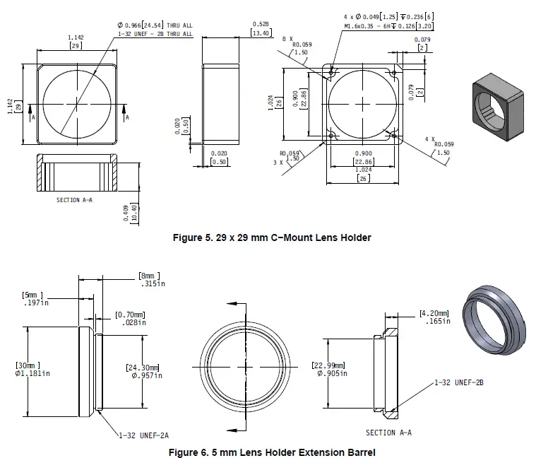
Lens Mount
The headboard comes with a standard C−mount lens holder that is screwed onto the board. The lens mount is made of black aluminum and fits in a 29 x 29 mm2 design, as shown in Figure 6.
The lens mount comes with a 5 mm C−Mount extender barrel, see Figure 6, to provide a focal distance of 17.4 mm to the sensor.
Tripod Mount
In order to mount the cable firmly to the provided headboard, two different aluminum mounting pieces are provided that serve a dual purpose. Both as tripod mount for the provided tripod, see Figure 7, and as FMC cable connector lock, see Figure 8, to secure your hardware connection. These pieces are connected by two M2.5 screws and nuts.
Tripod
The last part to make the development kit complete is a standard adjustable tripod to aim the image sensor in any direction that is desired.
Not Included: Lens and FPGA Development Platform
ON Semiconductor provides a suggested lens list compatible with the XGS products on the public product page. The development kit does not include a FPGA development platform as different needs require different platforms.
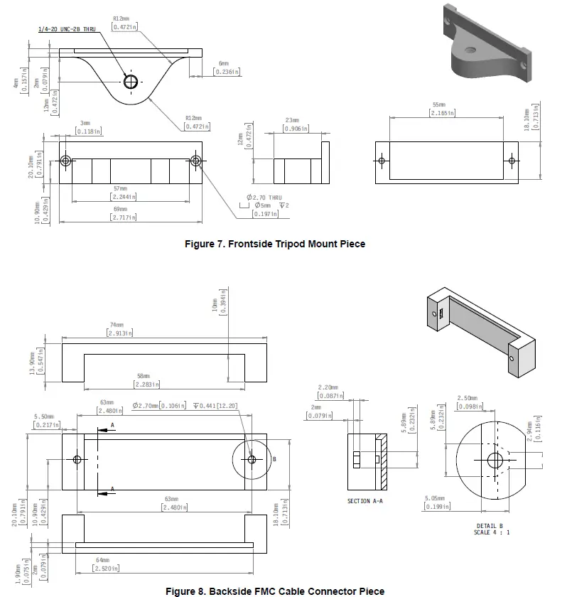
Table 2. X−CELERATOR BOM
| Item | Qty | Part Reference | Value | Package | Description | Manufacturer | Manufacturer Part Number |
| 1 | 8 | C1 C2 C3 C4 C7 C8 C28 C138 | 100 nF | 402 | CAP, CERAMIC, 100 nF, 16 V, X7R, 10%, 0402 | Murata | GRM155R71C104KA88D |
| 2 | 11 | C5 C9 C17 C33 C37 C41 C42 C69 C134 C135 C136 | 2.2 µF | 201 | CAP, CERAMIC, 2.2 µF, 10 V, X5R, 10%, 0201 | Murata | GRM033R61A225KE47D |
| 3 | 1 | C10 | 100 µF | 1210 | CAP, CERAMIC, 100 µF, 6.3 V, X5R, 20%, 1210 | Murata | GRM32ER60J107ME20L |
| 4 | 1 | C11 | 680 pF | 402 | CAP, CERAMIC, 680 pF, 25 V, X7R, 10%, 0402 | Panasonic | ECJ0EB1E681K |
| 5 | 1 | C12 | 12 nF | 402 | CAP, CERAMIC, 12 nF, 16 V, X7R, 10%, 0402 | Panasonic | ECJ0EB1C123K |
| 6 | 1 | C13 | 150 pF | 402 | CAP, CERAMIC, 150 pF, 25 V, X7R, 10%, 0402 | Panasonic | ECJ0EB1E151K |
| 7 | 1 | C14 | 10 nF | 402 | CAP, CERAMIC, 10 nF, 50 V, X6S, 10%, 0402 | TDK Corporation | C1005X6S1H103K |
| 8 | 1 | C15 | 100 µF | 7361−38 | CAP, TANTALUM CHIP, LOW ESR, 100 µ F, 25 V, 10%, 7361 | AVX | TPSV107K025R0100 |
| 9 | 27 | C16 C18 C19 C20 C21 C23 C24 C25 C27 C31 C49 C53 C68 C71 C80 C83 C84 C99 C100 C101 C102 C103 C104 C105 C113 C114 C130 | 10 µF | 402 | CAP, CERAMIC, 10 µF, 6.3 V, X5R, 20%, 0402 | Murata | GRM155R60J106ME15D |
| 10 | 6 | C22 C29 C39 C43 C45 C51 | 4.7 µF | 402 | CAP, CERAMIC, 4.7 µF, 6.3 V, X5R, 20%, 0402, Automotive AEC−Q200 | Taiyo Yuden | JMK105BBJ475MVHF |
| 11 | 64 | C26 C30 C32 C34 C35 C36 C38 C40 C44 C46 C47 C48 C50 C52 C54 C56 C57 C59 C60 C61 C62 C63 C64 C65 C66 C67 C79 C81 C82 C85 C86 C87 C88 C89 C90 C91 C92 C93 C94 C95 C96 C97 C98 C106 C107 C108 C109 C110 C111 C115 C116 C117 C118 C119 C120 C121 C122 C123 C124 C125 C126 C127 C128 C129 | 100 µF | 201 | CAP, CERAMIC, 100 nF, 10 V, X5R, 20%, 0201 | Panasonic | ECJZEB1A104M |
| 12 | 1 | FL1 | 1 µF | 603 | IND, EMI FILTER, CHIP, FERRITE BEAD, SMD, 1 µF, 2 A, 6.3 V, 0603 | Murata | NFM18PC105R0J3D |
| 13 | 1 | L1 | 1 µH | 98x79x35 | IND, POWER, MULTILAYER, SMD, 1.0 µH, 1.6 A, +/−20%, .098”L x .079”W x .035”H | Murata | LQM2HPN1R0MG0 |
| 14 | 1 | L3 | 5.6 µH | 254x262x240 | IND, POWER, SMD, 5.6 µH, 6.9 A, .254”L x .262”W x .240”H | Wurth ElectroniK | 74439346056 |
| 15 | 1 | P1 | HDR400−10×40−P | CONN, HEADER, SINGLE END ARRAY, 10×40, 400 PIN, 1.27 MM PITCH, ALGNMNT PINS, SMD | Samtec | ASP−134488−01 | |
| 16 | 1 | R2 | 24 K | 402 | RESISTOR, PRECISION THICK FILM CHIP, SMD, 24 K, 0.1 W, 1%, 0402, AEC−Q200 compliant | Panasonic | ERJ2RKF2402X |
| 17 | 2 | R3 R7 | 1 K | 402 | RESISTOR, PRECISION THICK FILM CHIP, SMD, 1 K, 0.1 W, 1%, 0402 , Automotive grade, AEC−Q200 compliant | Panasonic | ERJ−2RKF1001X |
| Item | Qty | Part Reference | Value | Package | Description | Manufacturer | Manufacturer Part Number |
| 18 | 1 | R4 | 14.7 K | 402 | RESISTOR, PRECISION THICK FILM CHIP, SMD, 14.7 KQ, 0.1 W, 1%, 0402, Automotive grade, AEC−Q200 compliant | Panasonic | ERJ−2RKF1472X |
| 19 | 1 | R5 | 8.06 K | 402 | RESISTOR, METAL THIN FILM CHIP, SMD, 8.06 K, 0.063 W, 0.1%, 0402 | Panasonic | ERA2AEB8061 |
| 20 | 1 | R6 | 0 | 603 | RESISTOR, THICK FILM CHIP, SMD, 0 Q JUMPER, 0.1 W, 5%, 0603, AEC−Q200 compliant | Panasonic | ERJ3GEY0R00V |
| 21 | 2 | R9 R10 | 10 K | 603 | RESISTOR, PRECISION THICK FILM CHIP, SMD, 10 K, 0.1 W, 1%, 0603 | Panasonic | ERJ3EKF1002V |
| 22 | 1 | R11 | 300 K | 402 | RESISTOR, PRECISION THICK FILM CHIP, SMD, 300 K, 0.1 W, 1%, 0402 | Panasonic | ERJ−2RKF3003 |
| 23 | 2 | R12 R13 | 0 | 402 | RESISTOR, PRECISION THICK FILM CHIP, SMD, 0 Q, 0.1 W, 1%, 0402, Automotive grade, AEC−Q200 compliant | Panasonic | ERJ2GE0R00X |
| 24 | 1 | R14 | 0 | 201 | RESISTOR, PRECISION THICK FILM CHIP, SMD, 0, 0.05 W, JUMPER, 0201, AEC−Q200 | Panasonic | ERJ1GN0R00C |
| 25 | 4 | R43 R44 R46 R47 | 100 | 201 | RESISTOR, PRECISION THICK FILM CHIP, SMD, 100 Q, 0.05 W, 1%, 0201 | Panasonic | ERJ1GEF1000C |
| 26 | 1 | R49 | 10 K | 402 | RESISTOR, THICK FILM CHIP, SMD, 10 K, 0.063 W, 5%, 0402, AEC−Q200 compliant | Panasonic | ERJ2GEJ103X |
| 27 | 2 | R50 R51 | 4.7 K | 402 | RESISTOR, THICK FILM CHIP, SMD, 4.7 K, 0.063 W, 5%, 0402 | Panasonic | ERJ2GEJ472X |
| 28 | 1 | R52 | 0 | 201 | RESISTOR, THICK FILM CHIP, SMD, 0 Q JUMPER, 0.05 W, 5%, 0201 | Panasonic | ERJ1GE0R00C |
| 29 | 4 | TP6 TP7 TP8 TP9 | TSTPT−5016 | CONN, TERMINAL, TEST POINT COMPACT, .015 THICK, SMT | Keystone Electronics | 5016 | |
| 30 | 1 | U1 | NOIX1SN012KB− LTI | LGA163 | IC, SENSOR, ACTIVE−PIXEL DIGITAL IMAGE, CMOS, XGS12M, LGA163 | ON Semiconductor | NOIX1SN012KB−LTI |
| 31 | 1 | U2 | CAT24C64 | SO8 | IC, SERIAL EEPROM, I2C, 64 Kbit, +1.7 V TO +5.5 V, −40°C to +85°C, SO8 Narrow | ON Semiconductor | CAT24C64WI−GT3 |
| 32 | 1 | U3 | NLSV8T244 | UDFN20 | IC, LEVEL TRANSLATOR, NON−INVERTING, DUAL SUPPLY, 8−BIT, 0.9 V TO 4.5 V, UDFN20 | ON Semiconductor | NLSV8T244MUTAG |
| 33 | 1 | U4 | NCP3170 | SO8 | IC, VOLTAGE REGULATOR, 500 kHz SYNCHRONOUS BUCK CONVERTER, 4.5 V TO 18 V IN, ADJUSTABLE OUT, 3 A, SO8 | ON Semiconductor | NCP3170ADR2G |
| 34 | 1 | U6 | NCP6914 | WLCSP20 | IC, PMIC, 5 CHANNEL, ONE DC-DC CONVERTER AND 4 LDOs, 2.3 V TO 5.5 V INPUT, WLCSP20 | ON Semiconductor | NCP6914AFCDT1G |
| Item | Qty | Part Reference | Value | Package | Description | Manufacturer | Manufacturer Part Number |
| 35 | 1 | U7 | PCA9654E | TSSOP16 | IC, I/O EXPANDER, I2C, 8−BIT, 1 MHz, 1.65 V TO 5.5 V, TSSOP16 | ON Semiconductor | PCA9654EDTR2G |
| 36 | 1 | U9 | 32 MHz | OSC, SPXO, 32 MHz, 50 ppm, SMD, 1.6 V − 3.6 V, 2.5 MM x 2.0 MM x 0.8 MM | SEIKO EPSON CORPORATION | SG−210STF 32.0000ML | |
| 37 | 1 | U10 | TMUX1104DGSR | VSSOP10 | IC, PRECISION MULTIPLEXER, 4:1, LOW LEAKAGE CURRENT, 1.08 V TO 5.5 V, VSSOP10 | Texas Instruments | TMUX1104DGSR |
| 38 | 1 | U11 | NLSV2T244 | UDFN8 | IC, LEVEL TRANSLATOR, NON−INVERTING, DUAL SUPPLY, 2−BIT, 0.9 V TO 4.5 V, UDFN8 | ON Semiconductor | NLSV2T244MUTAG |
FMC CONNECTION PINS
The High−pin Count (HPC) FMC connector, see Table 3, provides maximal compatibility for the X−Celebrator. This HPC connector is designed to mate with both LPC and HPC connectors on the carrier board. Table 4 demonstrates this by using only the C, D, G, H pin arrays for critical communication. Only 28 out of the 80 differential pairs on the HPC (34 on LPC) connector are being used to communicate with the sensor. The other pins are still available for additional development. For example, a display port module.
DELAWARE AS INTERFACING SOFTWARE LAYER
From DevWare version 6.0.38 onward, Delaware is able to recognize and interface with FPGA boards, that contain the latest X−Celerator bit files. With the RADON driver (found on MyON) installed, DevWare should automatically recognize the X−Celebrator on your FPGA board connected to the PC, the correct sensor INI file still needs to be selected (and downloaded from the image sensor portal) to load the latest register settings and demonstrate the best capabilities of the sensor.
Figure 9 shows a complete development platform setup using the X−Celerator development kit, an Edmund optics lens (not included) and a Xilinx Kintex UltraScale FPGA KCU105 evaluation kit. Please note that for most development needs this KCU105 evaluation kit is over−qualified and cheaper options are available.
Table 3. X−CELERATOR HPC FMC CONNECTOR
| Connector | Manufacturer | Part Number | Description |
| P1 | Samtec | ASP−134488−01 | CONN, HEADER, SINGLE END ARRAY, 10×40 400 PIN, 1.27 MM PITCH, ALGNMNT PINS, SMD |
Table 4. FMC CONNECTOR P1 PIN DESCRIPTION
| Pin No. | Dir | Function | Pin No. | Dir | Function |
| H16 | OUT | DATA_0_P | H17 | OUT | DATA_0_N |
| G15 | OUT | DATA_2_P | G16 | OUT | DATA_2_N |
| C14 | OUT | DATA_4_P | C15 | OUT | DATA_4_N |
| D14 | OUT | DATA_6_P | D15 | OUT | DATA_6_N |
| H13 | OUT | DATA_8_P | H14 | OUT | DATA_8_N |
| G12 | OUT | DATA_10_P | G13 | OUT | DATA_10_N |
| D11 | OUT | DATA_12_P | D12 | OUT | DATA_12_N |
| C10 | OUT | DATA_14_P | C11 | OUT | DATA_14_N |
| G9 | OUT | DATA_16_P | G10 | OUT | DATA_16_N |
| H10 | OUT | DATA_18_P | H11 | OUT | DATA_18_N |
| D8 | OUT | DATA_20_P | D9 | OUT | DATA_20_N |
| H7 | OUT | DATA_22_P | H8 | OUT | DATA_22_N |
| H31 | OUT | DATA_1_P | H32 | OUT | DATA_1_N |
| G30 | OUT | DATA_3_P | G31 | OUT | DATA_3_N |
| G27 | OUT | DATA_5_P | G28 | OUT | DATA_5_N |
| H28 | OUT | DATA_7_P | H29 | OUT | DATA_7_N |
| C26 | OUT | DATA_9_P | C27 | OUT | DATA_9_N |
| D26 | OUT | DATA_11_P | D27 | OUT | DATA_11_N |
| H25 | OUT | DATA_13_P | C26 | OUT | DATA_13_N |
| G24 | OUT | DATA_15_P | G25 | OUT | DATA_15_N |
| D23 | OUT | DATA_17_P | D24 | OUT | DATA_17_N |
| H22 | OUT | DATA_19_P | H23 | OUT | DATA_19_N |
| C22 | OUT | DATA_21_P | C23 | OUT | DATA_21_N |
| G21 | OUT | DATA_23_P | G22 | OUT | DATA_23_N |
| H4 | OUT | D_CLK_2_P | H5 | OUT | D_CLK_2_N |
| G2 | OUT | D_CLK_3_P | G3 | OUT | D_CLK_3_N |
| C35, C37 | PWR | 12 V FMC | C39, D36, D38, D40 | PWR | 3.3V FMC |
| F40, E39, G39, H40 | PWR | VADJ (for voltage convertor) | D32 | PWR | 3.3V_VAUX_FMC (EEPROM) |
| H1 | PWR | VREF_A_M2C | K1 | PWR | VREF_B_M2C |
| J39, K40 | PWR | VIO_B_M2C | H19 | IN | RESET_N_VADJ |
| H20 | IN | TRIGGER_INT_VADJ | G19 | IN | TRIGGER_RD_VADJ |
| D17 | IN | SCLK_VADJ | D18 | IN | SDATA_VADJ |
| C18 | IN | CS_N_VADJ | C19 | OUT | SDATAOUT_VADJ |
| C30 | IN | SCL (EEPROM) | C31 | IN / OUT | SDA (EEPROM) |
| C34 | IN | GA0 (EEPROM) | C35 | IN | GA1 (EEPROM) |
SPECIFICATIONS AND USEFUL REFERENCES
Detailed schematics, layout files, EEPROM bin content and FPGA bitfiles of the X−Celerator together with the sensor-specific DevWare software can be found under NDA on the image sensor portal.
The X−Celerator headboard outline was designed according to the ANSI/VITA 57.1 standard specifications. More information about this standard can be found at: https://www.samtec.com/standards/vita/fmc
The product page of ON Semiconductor XGS 5000, XGS 12000 and XGS 16000 image sensors contains the datasheet, lens list and other resources for these sensors.
More detailed technical information on the XGS 5000, XGS 12000 and XGS 16000 image sensors can be found in their respective developer guides, namely AND90031−D, AND9878−D and AND90029−D, which are also available on the image sensor portal under standard products → XGS. 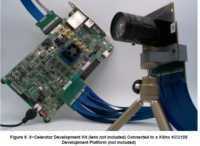
onsemi, , and other names, marks, and brands are registered and/or common law trademarks of Semiconductor Components Industries, LLC dba “onsemi” or its affiliates and/or subsidiaries in the United States and/or other countries. onsemi owns the rights to a number of patents, trademarks, copyrights, trade secrets, and other intellectual property. A listing of on semi’s product/patent coverage may be accessed at www.onsemi.com/site/pdf/Patent−Marking.pdf. onsemi is an Equal Opportunity/Affirmative Action Employer.
This literature is subject to all applicable copyright laws and is not for resale in any manner.
The evaluation board/kit (research and development board/kit) (hereinafter the “board”) is not a finished product and is not available for sale to consumers. The board is only intended for research, development, demonstration and evaluation purposes and will only be used in laboratory/development areas by persons with engineering/technical training and familiar with the risks associated with handling electrical/mechanical components, systems and subsystems. This person assumes full responsibility/liability for proper and safe handling. Any other use, resale or redistribution for any other purpose is strictly prohibited.
THE BOARD IS PROVIDED BY ONSEMI TO YOU “AS IS” AND WITHOUT ANY REPRESENTATIONS OR WARRANTIES WHATSOEVER. WITHOUT LIMITING THE FOREGOING, ONSEMI (AND ITS LICENSORS/SUPPLIERS) HEREBY DISCLAIMS ANY AND ALL REPRESENTATIONS AND WARRANTIES IN RELATION TO THE BOARD, ANY MODIFICATIONS, OR THIS AGREEMENT, WHETHER EXPRESS, IMPLIED, STATUTORY OR OTHERWISE, INCLUDING WITHOUT LIMITATION ANY AND ALL REPRESENTATIONS AND WARRANTIES OF MERCHANTABILITY, FITNESS FOR A PARTICULAR PURPOSE, TITLE, NON−INFRINGEMENT, AND THOSE ARISING FROM A COURSE OF DEALING, TRADE USAGE, TRADE CUSTOM OR TRADE PRACTICE.
onsemi reserves the right to make changes without further notice to any board.
You are responsible for determining whether the board will be suitable for your intended use or application or will achieve your intended results. Prior to using or distributing any systems that have been evaluated, designed or tested using the board, you agree to test and validate your design to confirm the functionality for your application. Any technical, applications or design information or advice, quality characterization, reliability data or other services provided by onsemi shall not constitute any representation or warranty by on semi, and no additional obligations or liabilities shall arise from onsemi having provided such information or services.
onsemi products including the boards are not designed, intended, or authorized for use in life support systems, or any FDA Class 3 medical devices or medical devices with a similar or equivalent classification in a foreign jurisdiction, or any devices intended for implantation in the human body. You agree to indemnify, defend and hold harmless onsemi, its directors, officers, employees, representatives, agents, subsidiaries, affiliates, distributors, and assigns, against any and all liabilities, losses, costs, damages, judgments, and expenses, arising out of any claim, demand, investigation, lawsuit, regulatory action or cause of action arising out of or associated with any unauthorized use, even if such claim alleges that onsemi was negligent regarding the design or manufacture of any products and/or the board.
This evaluation board/kit does not fall within the scope of the European Union directives regarding electromagnetic compatibility, restricted substances (RoHS), recycling (WEEE), FCC, CE or UL, and may not meet the technical requirements of these or other related directives.
FCC WARNING
This evaluation board/kit is intended for use for engineering development, demonstration, or evaluation purposes only and is not considered by onsemi to be a finished end product fit for general consumer use. It may generate, use, or radiate radio frequency energy and has not been tested for compliance with the limits of computing devices pursuant to part 15 of FCC rules, which are designed to provide reasonable protection against radio frequency interference. Operation of this equipment may cause interference with radio communications, in which case the user shall be responsible, at its expense, to take whatever measures may be required to correct this interference.
onsemi does not convey any license under its patent rights nor the rights of others.
LIMITATIONS OF LIABILITY:
onsemi shall not be liable for any special, consequential, incidental, indirect or punitive damages, including, but not limited to the costs of requalification, delay, loss of profits or goodwill, arising out of or in connection with the board, even if onsemi is advised of the possibility of such damages. In no event shall onsemi’s aggregate liability from any obligation arising out of or in connection with the board, under any theory of liability, exceed the purchase price paid for the board, if any.
The board is provided to you subject to the license and other terms per on semi’s standard terms and conditions of sale. For more information and documentation, please visit www.onsemi.com.
PUBLICATION ORDERING INFORMATION
LITERATURE FULFILLMENT:
Email Requests to: [email protected]
onsemi Website: www.onsemi.com
TECHNICAL SUPPORT
North American Technical Support:
Voice Mail: 1 800−282−9855 Toll-Free USA/Canada Phone: 011 421 33 790 2910
Europe, Middle East and Africa Technical Support:
Phone: 00421 33 790 2910
For additional information, please contact your local Sales Representative


