Suzhou Eiccomm Technology Turing Bluetooth Module
General Description
Turing Module is a SOC module developed based on the Telink TLSR8258F512ET chip. The Turing Module integrates a power-balanced 32-bit MCU, BLE/802.15.4/ 2.4GHz Radio, 64kB SRAM, 512kB internal Flash, 14bit ADC with PGA, analog and digital microphone input, stereo audio output, 6-channel PWM, one quadrature decoder (QDEC), abundant and flexible GPIO interfaces, and nearly all the peripherals needed for IoT (Internet of Things) and HID (Human Interface Devices) application development e.g. Bluetooth Low Energy and Zigbee/IEEE 802.15.4/RF4CE. The Turing Module supports standards and industrial alliance specifications including Bluetooth Low Energy up to Bluetooth 5, BLE Mesh, 6LoWPAN, Thread, Zigbee, RF4CE, HomeKit, ANT and 2.4GHz proprietary standard.
Block diagram
The TLSR8258 is designed to offer high integration, ultra-low power application capabilities. The system’s block diagram is as shown in following figure. 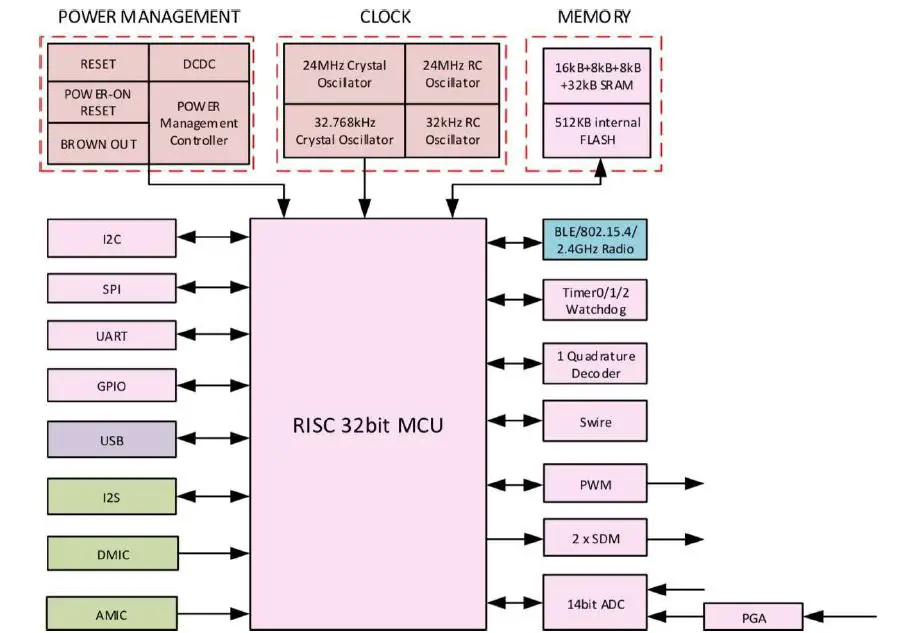 NOTE
NOTE
Modules marked with different colors belong to different power domains. Power state of each domain can be controlled independent of other power domains, for example, the audio module including I2S,DMIC,AMIC can be independently powered on or powered down irrespective of other modules such as power management module, clock, and etc. The BLE/802.15.4/2.4GHz Radio, USB and Audio I2S, DMIC, AMIC are powered down by default. The power management module and clock should be always powered on, even in deep sleep. In deep sleep, except for the power management and clock, all other modules should be powered down.
Key Features
- Bluetooth 5 Compliant, 1Mbps, 2Mbps, Long Range 125kbps and 500kbps
- IEEE802.15.4 compliant, 250kbps
- 2.4GHz proprietary 1Mbps/2Mbps/250kbps/500kbps mode with Adaptive
Frequency Hopping feature support
- 64kB on-chip SRAM with up to 32kB retention
- 512kB internal Flash
- A rich set of I/Os: SPI, I2C, USB, Single wire, up to 16 GPIOs, UART with hardware flow control,DMIC (Digital Mic) , AMIC (Analog Mic ),I2S, Stereo Audio output
- 6-channel PWM (Pulse Width Modulation) output
- 10-channel (only GPIO input), 14-bit SAR ADC with 10.5-bit ENOB
Electrical Specifications
The electrical characteristics currently listed in this section are target specifications and only supplied for reference. Some data may be updated according to actual test results.
Absolute Maximum Ratings
| Characteristics | Sym | Min | Max | Unit |
| Supply Voltage | VDD | -0.3 | 3.6 | V |
| Voltage on Input Pin | Vin | –0.3 | VDD+0.3 | V |
| Output Voltage | Vout | 0 | VDD | V |
| Storage Temperature Range | Tstr | -65 | 250 | ◦C |
| Soldering Temperature | slTd | 260 | ◦C |
CAUTION
Stresses above those listed in “Absolute Maximum Ratings” may cause permanent damage to the device. This is a stress only rating and operation of the device at these or any other conditions above those indicated in the operational sections of this specification is not implied
Recommended Operating Condition
| Item | Sym | Min | Typ | Max | Unit | Condition |
| Power supply Voltage | VDD | 1.8 | 3.3 | 3.6 | V | All AVDD,DVDD and VDD_IO pin must have the same voltage |
| Supply Rise Time from 1.6V to 1.8V | tR | 10 | ms | |||
| Operating Temperature Range | TOpr | -40 | 85 | ◦C | ET Version | |
| -40 | 125 | ◦C | AT Version |
DC characteristics
DC Characteristics (VDD=3.3V, T=25°C)
| Item | Sym | Min | Typ | Max | Unit | Condition |
| RX Current | IRx | 5.3 | mA | Whole Chip | ||
| TX Current | ITx | 4.8 | mA | Whole Chip@0dBm with DCDC | ||
| Deep Sleep with 8kB SRAM Retention | IDeep1 | 1 | uA | |||
| Deep Sleep with 16kB SRAM Retention | 1.2 | uA | ||||
| Deep Sleep with 32kB SRAM Retention | 1.4 | uA | ||||
| Deep Sleep without SRAM Retention | IDeep2 | 0.4 | uA |
RF Specifications
RF Performance
| Item | Sym | Min | Typ | Max | Unit | Condition |
| RF Frequency Range | 2380 | 2500 | MHz | Programmable in 1MHz Step | ||
| Date Rate | BLE/2.4G Proprietary 1Mbps, ±250kHz deviation BLE/2.4G Proprietary 2Mbps, ±500kHz deviation BLE 125kbps, ±250kHz deviation BLE 500kbps, ±250kHz deviation 802.15.4 250kbps, ±500kHz deviation 2.4G Proprietary 500kbps, ±125kHz deviation 2.4G Proprietary 250kbps, ±62.5kHz deviation | |||||
| Item | Sym | Min | Typ | Max | Unit | Condition |
| RX Sensitivity | 1Mbps | -96 | dBm | |||
| Frequency Offset Tolerance | -250 | +300 | kHz | |||
| TX power Maximum Setting | 10 | dBm | ||||
| TX power Minimum Setting | -45 | dBm | ||||
| Programmable output power range | 55 | Db | ||||
| Modulation 20dB Bandwidth | 2.5 | MHz | ||||
BLE 1Mbps performance (±250kHz deviation)
| Item | Sym | Min | Typ | Max | Unit | Condition |
| RX Sensitivity | 2Mbps | -93 | dBm | |||
| Frequency Offset Tolerance | -300 | +200 | kHz | |||
| TX power Maximum Setting | 10 | dBm | ||||
| TX power Minimum Setting | -45 | dBm | ||||
| Programmable output power range | 55 | Db | ||||
| Modulation 20dB Bandwidth | 1.4 | MHz | ||||
BLE 2Mbps performance (±500kHz deviation)
| Item | Sym | Min | Typ | Max | Unit | Condition |
| RX Sensitivity | 500kbps | -99 | dBm | |||
| Frequency Offset Tolerance | -150 | +50 | kHz | |||
| TX power Maximum Setting | 10 | dBm | ||||
| TX power Minimum Setting | -45 | dBm | ||||
| Programmable output power range | 55 | Db | ||||
| Modulation 20dB Bandwidth | 2.5 | MHz | ||||
BLE 500kbps performance (±250kHz deviation)
| Item | Sym | Min | Typ | Max | Unit | Condition |
| RX Sensitivity | 125kbps | -101 | dBm | |||
| Frequency Offset Tolerance | -150 | +50 | kHz | |||
| TX power Maximum Setting | 10 | dBm | ||||
| TX power Minimum Setting | -45 | dBm | ||||
| Programmable output power range | 55 | Db | ||||
| Modulation 20dB Bandwidth | 2.5 | MHz | ||||
BLE 125kbps performance (±250kHz deviation)
Hardware Design
Pin Definition
| Pin NO. | Pin Name | Type | Description |
| 1 | DVSS | GND | Digital LDO ground |
| 2 | SPI_CN/I2S_LR/PWM3/PD<2> | Digital I/O | SPI chip select (Active low) / I2S left right channel select / PWM3 output / GPIO PD[2] |
| 3 | PWM1_N/I2S_SDI/7816_TRX(UART_TX)/PD< 3> | Digital I/O | PWM1 inverting output / I2S serial data input / UART 7816 TRX(UART_TX) / GPIO PD[3] |
| 4 | SWM/I2S_SDO/PWM2_N/PD<4> | Digital I/O | Single wire master / I2S serial data output / PWM2 inverting output / GPIO PD[4] |
| 5 | SPI_CK/I2S_BCK/7816_TRX(UART_TX)/ PD<7> | Digital I/O | SPI clock(I2C_SCK) / I2S bit clock / UART 7816 TRX(UART_tx) / GPIIO PD[7] |
| 6 | DMIC_DI/PWM0_N/UART_RX/PA<0> | Digital I/O | DMIC data input / PWM0 inverting output / UART_RX / GPIO PA[0] |
| 7 | PWM4/UART_TX/Iccopmpain<1>/ saraio<1>/PB<1> | Digital I/O | PWM4 output / UART_TX / Low power comparator input / SAR ADC input / GPIO PB[1] |
| 8 | DVSS | GND | Digital LDO ground |
| 9 | SWS/UART_RTS/PA<7> | Digital I/O | Single wire slave/ UART_RTS / GPIO PA[7] |
| 10 | VDD_IO | PWR | External 3.3V power supply input for IO |
| 11 | SDM_P0/PWM4/lccompain<4>/ saraio<4>/PB<4> | Digital I/O | SDM positive output 0 / PWM4 output / Low power comparator input / SAR ADC input / GPIO PB[4] |
| 12 | SDM_N0/PWM5/lccomp_ain<5>/ saraio<5>/PB<5> | Digital I/O | SDM negative output 0 / PWM5 output / Low power comparator input / SAR ADC input / GPIO PB[5] |
| 13 | SDM_P1/SPI_DI/UART_RTS/ lccompain<6>/saraio<6>/ PB<6> | Digital I/O | SDM positive output 1 / SPI data input (I2C_SDA) / UART_RTS / Low power comparator input / SAR ADC input / GPIO PB[6] |
| 14 | SDM_N1/SPI_DO/UART_RX/ lccompain<7>/saraio<7>/ PB<7> | Digital I/O | SDM negative output 1 / SPI data output / UART_RX / Low power comparator input / SAR ADC input / GPIO PB[7] |
| 15 | I2C_SDA/PWM4_N/UART_RTS/
PGA_P0/PC<0> | Digital I/O | I2C serial data / PWM4 inverting output / UART_RTS /
PGA left channel positive input / GPIO PC[0] |
| 16 | I2C_SCK/PWM1_N/PWM0/ PGA_N0/PC<1> | Digital I/O | I2C serial clock / PWM1 inverting output / PWM0 output / PGA left channel negative input / GPIO PC[1] |
| 17 | PWM0/7816_TRX(UART_TX)/I2C_SDA/XC32K _O/PGA_P1/PC<2> |
Digital I/O | PWM0 output / UART 7816 TRX (UART_TX) / I2C serial data / (optional) 32kHz crystal output / PGA right channel positive input / GPIO PC[2] |
| 18 | PWM1/UART_RX/I2C_SCK/XC32K_ I/PGA_N1/PC<3> |
Digital I/O | PWM1 output / UART_RX / I2C serial clock / (optional) 32kHz crystal input / PGA right channel negative input / GPIO PC[3] |
| 19 | PWM2/UART_CTS/PWM0_N/ saraio<8>/PC<4> | Digital I/O | PWM2 output / UART_CTS / PWM0 inverting output / SAR ADC input / GPIO PC[4] |
| 20 | DVSS | GND | Digital LDO ground |
Pin Definition
- All digital IOs including PA<0> ~ PD<7> can be used as GPIOs and have configurable pull-up/pulldown resistor.
- SPI:
- PD<7>: SPI_CK, PB<6>: SPI_DI, PB<7>: SPI_DO, PD<2>: SPI_CN
- PA<2>: DO, PA<3>: DI, PA<4>: CK, PD<6>: CN 3
I2C:PC<0> ~ PC<3> can be used as I2C. PC<0>: I2C_SDA, PC<1>: I2C_SCK,PC<2>: I2C_SDA, PC<3>: I2C_SCK - I2C can also be multiplexed with SPI interface, i.e. I2C_SDA/I2C_SCK can be multiplexed with SPI_DI /SPI_CK respectively.
- Audio PGA/AMIC input: PC<0>~PC<3>. Any GPIO pin can be used as AMIC BIAS.
- DMIC: PA<0>: DMIC_DI, PA<1>: DMIC_CLK
- I2S: PD<7>: I2S_BCK, PA<1>: I2S_CLK, PD<2>: I2S_LR, PD<3>: I2S_SDI, PD<4>: I2S_SDO
- Stereo audio output: PB<4>: SDM_P0, PB<5>: SDM_N0, PB<6>: SDM_P1, PB<7>: SDM_N1
- UART: PA<0>: UART_RX, PA<2>: UART_TX, PB<0>: UART_RX, PB<1>: UART_TX, PB<7>: UART_RX, PC<3>: UART_RX PC<5>:UART_RX, PD<6>: UART_RX
- UART hardware flow control: PA<3>: UART_CTS, PA<4>: UART_RTS, PA<7>: UART_RTS, PB<2>: UART_CTS, PB<3>: UART_RTS, PB<6>:UART_RTS, PC<0>: UART_RTS, PC<4>: UART_CTS, PD<1>: UART_CTS
- UART 7816: PD<7>: 7816_TRX (UART_TX), PA<1>: 7816_CLK, PC<2>: 7816_TRX (UART_TX), PD<0>: 7816_TRX (UART_TX), PD<3>:7816_TRX (UART_TX)
- USB: PA<5>: DM
- PA<6>: DP
- Single Wire debug interface: PA<7>: SWS. SWS can also be multiplexed with DP PD<4>: SWM
- RX_CYC2LNA & TX_CYC2PA: PB<2>: RX_CYC2LNA, PB<3>: TX_CYC2PA, PC<6>: RX_CYC2LNA, PC<7>:TX_CYC2PA, PD<0>:RX_CYC2LNA, PD<1>: TX_CYC2PA
- RX_CYC2LNA/TX_CYC2PA serves to control enabling external PA/LNA.
- ATSEL0~2: PB<0>: ATSEL1, PB<1>: ATSEL2, PC<5>: ATSEL0, PC<6>: ATSEL1, PC<7>: ATSEL2, PD<6>: ATSEL0
- ATSEL0~2 serves to select one of up to eight external antennas connected to the antenna select component. The selected antenna channel is connected to the RF_IO pin.
- Low power comparator input: PB<1>~ PB<7>.
- ADC GPIO input: PB<0>~ PB<7>, PC<4>~ PC<5>
- For 24MHz crystal, the load capacitor range supported by design is 7.33pF~12.66pF. If the crystal needs load capacitor of 15pF, two external capacitors will be required.
- Do not use PC<7:5> for dynamic applications. It’s highly recommended to use these IOs in DC applications, e.g. as control or detect lines.
- Pin drive strength: PA<5:7> and PB<0:3> support drive strength up to 8mA (8mA when “DS”=1, 4mA when “DS”=0); PB<4:7> support drive strength up to 16mA (16mA when DS=1, 12mA when “DS”=0); other GPIOs (PA<0:4>, PC<0:7> and PD<0:7>) support drive strength up to 4mA (4mA when “DS”=1, 2mA when DS=0).
- DS configuration will take effect when the pin is used as output.
Reference Design
The latest schematic and design examples, bill of material, and layout file are available from original developer. Contact us for details.
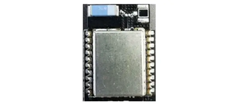
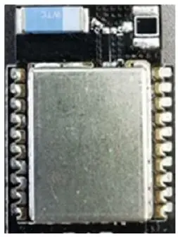
Appearance and Dimensions
The following picuture shows the appearance and dimensions of the module. The components and prominent structure are not allowed put in this size range.
Module Appearance
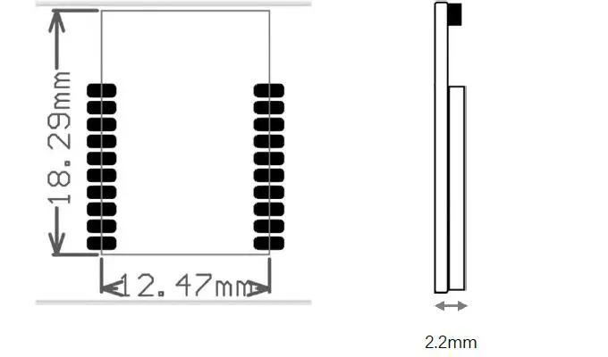
Module Dimensions
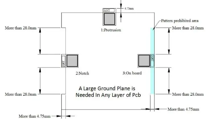
Layout Guideline
The layout on user PCB should be designed according to the following guide line.
Package
Module Packaging
Tray package.
Module Label
BLE module label on shield case combines QR code and plain text.
QR Code
There is a QR Code label in each product, which show device type and address infomation. QR code format:< mac address > # < module label >
Label demo shows in following picture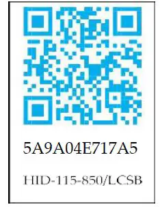
Welding Declare
The Turing module only supports one reflow soldering, and the module failure caused by multiple reflow soldering is not responsible.
Standard Operation Procedure (SOP)
This device complies with Part 15 of the FCC Rules. Operation is subject to the following two conditions this device may not cause harmful interference, and this device must accept any interference received, including interference that may cause undesired operation. Changes or modifications to this unit not expressly approved by the party responsible for compliance could void the user’s authority to operate the equipment.
NOTE
This equipment has been tested and found to comply with the limits for a Class B digital device, pursuant to Part 15 of the FCC Rules. These limits are designed to provide reasonable protection against harmful interference in a residential installation. This equipment generates, uses and can radiate radio frequency energy and, if not installed and used in accordance with the instructions, may cause harmful interference to radio communications. However, there is no guarantee that interference will not occur in a particular installation. If this equipment does cause harmful interference to radio or television reception, which can be determined by turning the equipment off and on, the user is encouraged to try to correct the interference by one or more of the following measures
- Reorient or relocate the receiving antenna.
- Increase the separation between the equipment and receiver.
- Connect the equipment into an outlet on a circuit different from that to which the receiver is connected.
- Consult the dealer or an experienced radio/TV technician for help.
This device and its antenna( must not be co-located or operation in conjunction with any other antenna or transmitter.
Radiation Exposure Statement
The device has been evaluated to meet general RF exposure requirement. in portable exposure condition without restriction.
Important Note
In the event that these conditions cannot be met (for example certain laptop configurations or co-location with another transmitter), then the FCC authorization is no longer considered valid and the FCC ID cannot be used on the final product. In these circumstances, the OEM integrator will be responsible for re-evaluating the end product (including the transmitter) and obtaining a separate FCC authorization. The OEM integrator has to be aware not to provide information to the end user regarding how to install or remove this RF module in the user’s manual of the end product which integrates this module.
Integration instructions for host product manufacturers according to KDB 996369 D03 OEM
List of applicable FCC rules
CFR 47 FCC PART 15 SUBPART C has been investigated. It is applicable to the modular.
Specific operational use conditions
This module is stand-alone modular. If the end product will involve the Multiple simultaneously transmitting condition or different operational conditions for a stand-alone modular transmitter in a host, host manufacturer have to consult with module manufacturer for the installation method in end system.
Limited module procedures
Not Applicable
Trace antenna designs
Not applicable
RF exposure considerations
The device has been evaluated to meet general RF exposure requirement. in portable exposure condition without restriction.
Antennas
This radio transmitter FCC ID: 2AXD8TURING has been approved by Federal Communications Commission to operate with the antenna types listed below, with the maximum permissible gain indicated. Antenna types not included in this list that have a gain greater than the maximum gain indicated for any type listed are strictly prohibited for use with this device.
| Internal Identification | Antenna Description | Antenna type and antenna number | Operate frequency band | Maximum antenna gain |
| Antenna 1 | Bluetooth Antenna | Chip Antenna | 2400 MHz – 2500 MHz | 0.92 dBi |
| Antenna 2 | Bluetooth Antenna | FPC Antenna | 2400 MHz – 2500 MHz | 1.65 dBi |
Label and compliance information
The final end product must be labeled in a visible area with the following Contains FCC ID: 2AXD8TURING
Information on test modes and additional testing requirements
Host manufacturer is strongly recommended to confirm compliance with FCC requirements for the transmitter when the module is installed in the host..
Additional testing, Part 15 Subpart B disclaimer
Host manufacturer is responsible for compliance of the host system with module installed with all other applicable requirements for the system.


