![]() USER MANUAL
USER MANUAL
T203PM100-MU
T203PM300-MU
T203PM600-MU
SINGLE-PHASE AC / DC TRUE RMS POWER METER
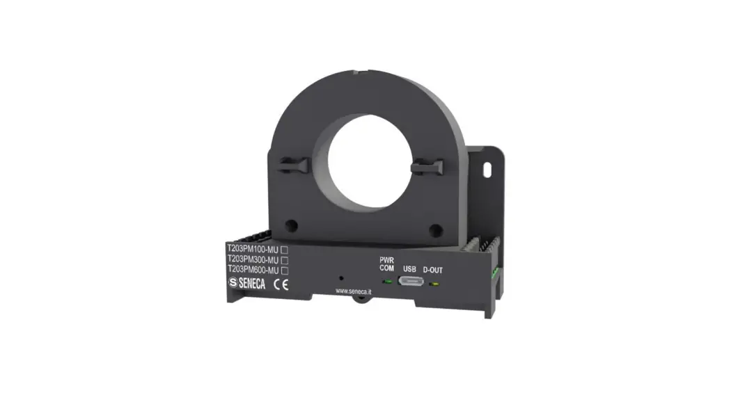
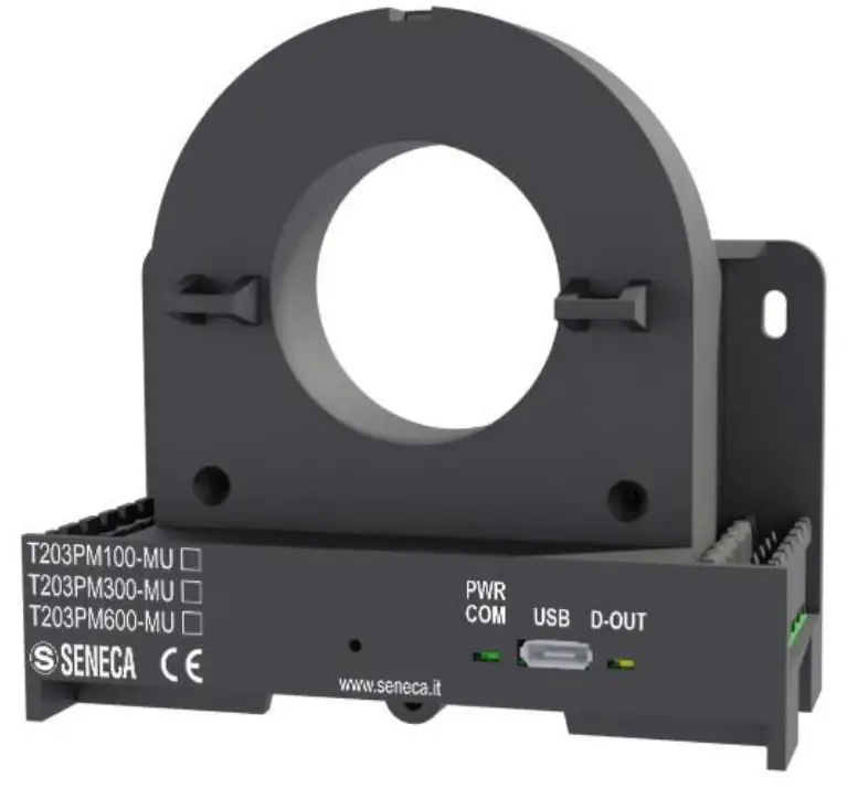
T203PM100-MU Single-Phase Ac / Dc True Rms Power Meter
WITH MODBUS RTU PROTOCOL AND ANALOGUE AND DIGITAL OUTPUTS
RIGINAL INSTRUCTIONS
The content of this documentation refers to products and technologies described in it.
All technical data contained in the document may be changed without notice.
The content of this documentation is subject to periodic review.
To use the product safely and effectively, read the following instructions carefully before use.
The product must be used only for the use for which it was designed and manufactured: any other use is under the full responsibility of the user.
Installation, programming and set-up are allowed only to authorized, physically and intellectually suitable operators.
Set-up must be performed only after correct installation and the user must follow all the operations described in the installation manual carefully.
Seneca is not responsible for failures, breakages and accidents caused by ignorance or failure to apply the stated requirements.
Seneca is not responsible for any unauthorized modifications.
Seneca reserves the right to modify the device, for any commercial or construction requirement, without the obligation to promptly update the reference manuals.
No liability for the contents of this document can be accepted.
Use the concepts, examples and other content at your own risk.
There may be errors and inaccuracies in this document that could damage your system, so proceed with caution, the author(s) will not take responsibility for it.
Technical specifications are subject to change without notice.
| CONTACT US | |
| Technical support | [email protected] |
| Product information | [email protected] |
This document is the property of SENECA srl. Copies and reproduction are prohibited unless authorised
Document revisions
| DATE | REVISION | NOTES | AUTHOR |
| 07/04/2021 | 0 | First revision | ET, MM |
| 25/06/2021 | 2 | Added Energy Counter Pulse info | ET, MM |
INTRODUCTION
![]() ATTENTION!
ATTENTION!
This user manual extends the information from the installation manual to the configuration of the device. Use the installation manual for more information.![]() ATTENTION!
ATTENTION!
In any case, SENECA s.r.l. or its suppliers will not be responsible for the loss of data/revenue or consequential or incidental damages due to negligence or bad/improper management of the device, even if SENECA is well aware of these possible damages. SENECA, its subsidiaries, affiliates, group companies, suppliers and distributors do not guarantee that the functions fully meet the customer’s expectations or that the device, firmware and software should have no errors or operate continuously.
1.1. DESCRIPTION
T203PM is a transducer for measuring AC/DC current and voltage in an isolated way (insulation relating to the communication ports and the analogue and digital output), aimed at measuring energy (bidirectionally) that can be installed on DIN 46277 rail.
| Model | Description | Communication protocols |
| T203PM-MU | ModBUS 1PH Power Meter with analogue and digital output | ModBUS RTU |
Measuring the voltage and current of the network, the instrument allows to measure the RMS values, instantaneous powers and energies of the devices to be monitored.
The 1.3kHz input measurement band guarantees the measurement of voltage and currents with harmonic components up to the twenty-first (at the mains frequency of 60 Hz). The use of this device is compatible with single-phase inverters.
The list of measurements made available by the tool is provided below:
- TRUE RMS AC VOLTAGE and CURRENT MEASUREMENTS (TRUE EFFECTIVE VALUE)
- DC VOLTAGE and BIPOLAR DC CURRENT MEASUREMENTS (the current can take on the +/- signs)
- MEASUREMENTS OF INSTANT POWER and ACTIVE, REACTIVE AND APPARENT ENERGY
- POWER FACTOR
- THD (AT NETWORK FREQUENCIES of 50 or 60 Hz)
- NETWORK FREQUENCY
The measured energies are stored in non-volatile memory cyclically once per second. For further information refer to the paragraph on ENERGY METERS
1.2. COMMUNICATION PORT SPECIFICATIONS
| RS485 COMMUNICATION PORTS | |
| Number | 1 |
| Baudrate | From 2400 to 115200 bit/s configurable |
| Parity, Data bit, Stop bit | Configurable |
| Protocol | ModBUS RTU Slave |
| USB COMMUNICATION PORT | |
| Number | 1 |
| Protocol | ModBUS RTU Slave |
| Use | For configuration with Easy-setup software and firmware update |
MEASURES AVAILABLE FROM SERIAL
2.1. CONVENTIONS
The device provides the measurement values of the powers on all 4 quadrants. The conventions for the signs of the measurements used in the product are summarized in the following image:
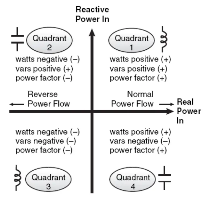
Where:
quadrant Q1 relates to an inductive load with imported (absorbed) active energy, classic use case.
quadrant Q2 relates to a capacitive load with exported (generated) active energy.
quadrant Q3 relates to an inductive load with exported (generated) active energy.
quadrant Q4 relates to a capacitive load with imported (absorbed) active energy.
2.2. INSTANTANEOUS VALUES PROVIDED and MINIMUM -MAXIMUM ABSOLUTE VALUES
The following table provides the list of instant measurements provided by the instrument; all instantaneous measurements have a minimum and maximum memory that can be reset via the ModBUS CLEAR MIN/MAX command (refer to the COMMAND register in the register list)
| Voltage | V |
| AC/DC (+/-) current | I |
| Active power (+/-) | P |
| Reactive power (+/-) | Q |
| Apparent power (+/-) | S |
| Power Factor | PF |
| Frequency | F (frequency measured on the mains voltage) |
| THD | % (measured on current) |
2.3. ENERGY METERS and INITIAL SETTINGS
The following table lists the 64-bit integer counters whose values are saved in Fe-RAM (memory writable an unlimited number of times):
| ACTIVE ENERGY [Wh/10] (TOTAL (+/-)) |
| REACTIVE ENERGY [VARh/10] (TOTAL (+/-)) |
| APPARENT ENERGY [VAh/10] (TOTAL (+/-)) |
To these 64-bit counters corresponds the value of the energies in 32-bit floating point value as shown in the following table (refer to the table of ModBUS registers at the end of the manual):
| MEASUREMENT | 64BIT INTEGER REGISTER | FLOAT32 REGISTER |
| ACTIVE ENERGY | EN_INT_ACTIVE [Wh/10] | MISEN_F_ACTIVE [Wh] |
| REACTIVE ENERGY | EN_INT_REACTIVE [VARh/10] | MISEN_F_REACTIVE [VARh] |
| APPARENT ENERGY | EN_INT_APPARENT [VAh/10] | MISEN_F_APPARENT [VAh] |
The ability to customize the 64-bit energy values is also made available to the user by following the following procedure which uses the sending of ModBUS commands to first unlock the write protection and then to finalize the writing in non-volatile memory:
- In the COMMAND register, send the ENABLE WRITE CUSTOM ENERGIES command
- Now the instrument no longer integrates the energies into memory; it is therefore possible to write the desired initial values in the 64bit integer registers relating to the ACTIVE / REACTIVE / APPARENT energies
- At this point it is possible to complete the writing using the ModBUS WRITE CUSTOM ENERGIES AND REBOOT command.
If, on the other hand, one only wishes to bring the values of these counters to zero, execute the ModBUS CLEAR ENERGIES command
Note:
- During normal operation, energies are saved in non-volatile memory once per second
- When customizing the energies, once the non-volatile write protection has been disabled, the device can return to normal operation using the ModBUS WRITE CUSTOM ENERGIES AND REBOOT or REBOOT commands.
EASUREMENT AND CALCULATION TIMES
3.1. SAMPLING TIMES
The sampling time of the current and voltage channels is 47000 samples per second.
The number of equivalent bits of the detected measurements is 13.5 bits
3.2. RESPONSE TIMES FOR RMS VALUES
We define the settling time as the time required for the RMS value to reach 99.5% of the full scale in response to an input from 0% to 100% of the full scale.
| DC measurements | AC measurements | |
| Settling time | 500 ms max | 1000 ms max |
| Rise time | <250ms | <250ms |
| Fall time | <250ms | <250ms |
3.3. RESPONSE TIMES OF THE ANALOGUE AND MODBUS OUTPUTS
Analogue Output Response Time: Typical 100ms (10-90%)
Modbus Response Time: Typical 5 ms
MEASUREMENT PRECISION AT 23°C
| Type of measurement | Precision at 23°C |
| Current RMS | 1% |
| RMS voltage | 1% |
| Powers / Energies | 1% |
| THD | 1% |
| Analogue output voltage | 0.2% +0.05V |
DEVICE CONFIGURATION
![]() ATTENTION!
ATTENTION!
TO CONFIGURE THE DEVICE USE THE EASY SETUP 2 SOFTWARE
Measurements provided by the device are subject to the user settings. The meaning of the device configuration registers that act on the electrical measurements performed is listed below (refer to the ModBUS registers at the end of the manual):
| MODBUS REGISTER | DESCRIPTION | DEFAULT VALUE |
| USR_MULTV | Set TV multiplication factor | 1 |
| USR_MULTI | Set TA multiplication factor | 1 |
| USR_TVRATIO | Set TV ratio factor | 1 |
| USR_AMPCUTOFF | Current cut-off value (zero = disabled) | 0 |
| USR_VOLTCUTOFF | Current cut-off value (zero = disabled) | 0 |
4.1. ANALOGUE AND DIGITAL OUTPUT
The analogue and digital outputs can be associated respectively to one of the instantaneous measurements provided between VOLTAGE / CURRENT / ACTIVE P. / REACTIVE P. / APPARENT P./ FREQUENCY / PF / THD. Below you can see the configuration details separately for the analogue and digital output.
4.1.1. Analogue output
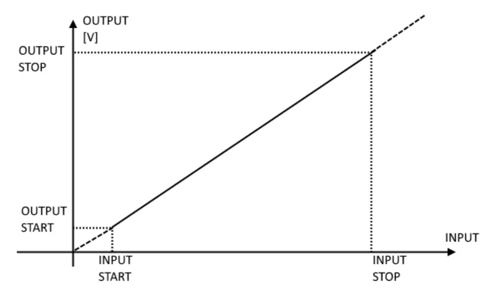
The analogue output is able to provide a voltage in the 0 ÷ 10V range; the analogue repetition of a measurement is performed by defining:
- A range of the input measurement (beginning and end of the measurement scale)
- A range of the output voltage to which the measurement will be associated (Start and end of the output scale)
The image below graphically illustrates the values described above
| MODBUS REGISTERS RELATING TO THE ANALOGUE OUTPUT | |
| MODBUS REGISTER | DESCRIPTION |
| USR_ALARMTYPE_AO DO | Select the type of measurement that can be combined [V, A, W, VAR, VA, Hz, PF, THD] |
| USRRO_AO_OUTPUTVOLTAGE | Value of the analogue voltage generated at the output |
| USR_AO_STARTINSCALE | Initial value of the measurement to be repeated [V, A, W, VAR, VA, Hz, PF, THD] |
| USR_AO_STOPINSCALE | Final value of the measurement to be repeated [V, A, W, VAR, VA, Hz, PF, THD] |
| USR_AO_STARTVOLTOUT | Minimum value of the output voltage associated with the start of the measurement scale |
| USR_AO_STOPVOLTOUT | Maximum value of the output voltage associated with the end of the measurement scale |
4.1.2. Digital output
The digital output is used for signalling alarms that may occur for a given measurement associated with it combined or for generating pulses related to the measured energy(*).
Below is a table with a brief description of the fields necessary to configure the digital output:
| MODBUS REGISTERS RELATING TO THE DIGITAL OUTPUT | |
| MODBUS REGISTER | DESCRIPTION |
| USR_ALARMTYPE_AO DO | Select the type of measurement that can be combined [V, A, W, VAR, VA, Hz, PF, THD] |
| USR_ALARM_DO_BEHAVIOUR | Behaviour of the alarm: NONE / MAX / MIN / INSIDE WINDOW/ OUTSIDE WINDOW / PULSES GENERATION: 1000 – 100 – 10 – 1 PULSES/kWh, 100 – 10 -1 PULSES/MWh (*) |
| USR_DO_ALNORMALLYHIGH | Set output as normally high or low |
| USR_DO_LOWVAL | Minimum alarm threshold of the measurement [V, A, W, VAR, VA, Hz, PF, THD] |
| USR_DO_HIGHVAL | Maximum alarm threshold of measurement [V, A, W, VAR, VA, Hz, PF, THD] |
| USR_DO_HIST | Hysteresis value of the min/max thresholds [V, A, W, VAR, VA, Hz, PF, THD] |
| USR_DO_TIMER10MS | Time spent in the alarm situation. The alarm is confirmed when this time is exceeded (multiples of 10ms) |
| USRRO_DO_ALSTATUS | Current alarm signalling: NO ALARM , MIN – MAX threshold PREALARM – INSIDE WINDOW – OUTSIDE WINDOW , MIN – MAX ALARM – INSIDE WINDOW – OUTSIDE WINDOW. (For numerical values refer to the list of ModBUS registers) |
(*): The pulse duration is 50ms ± 10ms, the pulse generation is relative to the active energy.
USB CONNECTION and CONFIGURATION RESET
The front USB port allows a simple connection to configure the device via the configuration software.
If it is necessary to restore the instrument’s initial configuration, use the configuration software.
FIRMWARE UPDATE
It is possible to update the firmware through the USB port (for more information refer to the Easy Setup 2 software)
MODBUS COMMUNICATION PROTOCOL
The supported communication protocol is:
- Modbus RTU Slave (from both the RS485 and USB ports)
For more information on these protocols, see the website: http://www.modbus.org/specs.php.
7.1. SUPPORTED MODBUS FUNCTION CODES
The following ModBUS functions are supported:
- Read Holding Register (function 3)
- Write Single Register (function 6)
- Write Multiple registers (function 16)
![]() ATTENTION!
ATTENTION!
All 32-bit values are contained in 2 consecutive registers![]() ATTENTION!
ATTENTION!
All 64-bit values are contained in 4 consecutive registers![]() ATTENTION!
ATTENTION!
Any registers with RW* (in flash memory) can be written up to about 10000 times The PLC/Master ModBUS programmer must not exceed this limit
MODBUS REGISTER TABLE
The following abbreviations are used in the register tables:
| MS | Most Significant |
| LS | Least Significant |
| MSBIT | Most Significant Bit |
| LSBIT | Least Significant Bit |
| MMSW | “Most” Most Significant Word (16bit ) |
| MSW | Most Significant Word (16bit ) |
| LSW | Least Significant Word (16bit) |
| LLSW | “Least” Least Significant Word (16bit) |
| RO | Read Only |
| RW* | Read-Write: REGISTERS IN FLASH MEMORY: WRITABLE ABOUT 10,000 TIMES MAXIMUM |
| RW** | Read-Write: REGISTERS THAT CAN BE WRITTEN ONLY AFTER WRITING THE “ENABLE WRITE CUSTOM ENERGIES = 49616” COMMAND |
| UNSIGNED 16 BIT | Integer register without sign that can take values from 0 to 65535 |
| SIGNED 16 BIT | Integer register with sign that can take values from -32768 to +32767 |
| UNSIGNED 32 BIT | Integer register without sign that can take values from 0 to 4294967296 |
| SIGNED 32 BIT | Integer register with sign that can take values from -2147483648 to 2147483647 |
| UNSIGNED 64 BIT | Integer register without sign that can take values from 0 to 18,446,744,073,709,551,615 |
| SIGNED 64 BIT | Integer register with sign that can assume values from -2^63 to 2^63-1 |
| FLOAT 32 BIT | 32-bit, single-precision floating-point register (IEEE54) https://en.wikipedia.org/wiki/IEEE_754 |
| BIT | Boolean register, which can take the values 0 (false) or 1 (true) |
8.1. NUMBERING OF “0-BASED” OR “1-BASED” MODBUS ADDRESSES
According to the ModBUS standard the Holding Registers are addressable from 0 to 65535, there are 2 different conventions for numbering the addresses: “0-BASED” and “1-BASED”. For greater clarity, Seneca shows its register tables in both conventions.
ATTENTION!
CAREFULLY READ THE DOCUMENTATION OF THE MODBUS MASTER DEVICE IN ORDER TO UNDERSTAND WHICH OF THE TWO CONVENTIONS THE MANUFACTURER HAS DECIDED TO USE
8.2. NUMBERING OF MODBUS ADDRESSES WITH “0-BASED” CONVENTION
The numbering is:
| HOLDING REGISTER MODBUS ADDRESS (OFFSET) | MEANING |
| 0 | FIRST REGISTER |
| 1 | SECOND REGISTER |
| 2 | THIRD REGISTER |
| 3 | FOURTH REGISTER |
| 4 | FIFTH REGISTER |
Therefore the first register is at address 0.
In the following tables, this convention is indicated with “ADDRESS OFFSET”.
8.3. NUMBERING OF MODBUS ADDRESSES WITH “1 BASED” CONVENTION (STANDARD)
The numbering is that established by the Modbus consortium and is of the type:
| HOLDING REGISTER MODBUS ADDRESS 4x | MEANING |
| 40001 | FIRST REGISTER |
| 40002 | SECOND REGISTER |
| 40003 | THIRD REGISTER |
| 40004 | FOURTH REGISTER |
| 40005 | FIFTH REGISTER |
In the following tables this convention is indicated with “ADDRESS 4x” since a 4 is added to the address so that the first Modbus register is 40001.
A further convention is also possible where the number 4 is omitted in front of the register address:
| HOLDING MODBUS ADDRESS WITHOUT 4x | MEANING |
| 1 | FIRST REGISTER |
| 2 | SECOND REGISTER |
| 3 | THIRD REGISTER |
| 4 | FOURTH REGISTER |
| 5 | FIFTH REGISTER |
8.4. BIT CONVENTION WITHIN A MODBUS HOLDING REGISTER
A Modbus Holding Register consists of 16 bits with the following convention:
| BIT 15 | BIT 14 | BIT 13 | BIT 12 | BIT 11 | BIT 10 | BIT 9 | BIT 8 | BIT 7 | BIT 6 | BIT 5 | BIT 4 | BIT 3 | BIT 2 | BIT 1 | BIT 0 |
For instance, if the value of the register in decimal is 12300
the value 12300 in hexadecimal is: 0x300C the hexadecimal 0x300C in binary value is: 11 0000 0000 1100
So, using the above convention, we get:
| BIT 15 | BIT 14 | BIT 13 | BIT 12 | BIT 11 | BIT 10 | BIT 9 | BIT 8 | BIT 7 | BIT 6 | BIT 5 | BIT 4 | BIT 3 | BIT 2 | BIT 1 | BIT 0 |
| 0 | 0 | 1 | 1 | 0 | 0 | 0 | 0 | 0 | 0 | 0 | 0 | 1 | 1 | 0 | 0 |
8.5. MSB and LSB BYTE CONVENTION WITHIN A MODBUS HOLDING REGISTER
A Modbus Holding Register consists of 16 bits with the following convention:
| BIT 15 | BIT 14 | BIT 13 | BIT 12 | BIT 11 | BIT 10 | BIT 9 | BIT 8 | BIT 7 | BIT 6 | BIT 5 | BIT 4 | BIT 3 | BIT 2 | BIT 1 | BIT 0 |
LSB Byte (Least Significant Byte) defines the 8 bits ranging from Bit 0 to Bit 7 included, we define MSB Byte (Most Significant Byte) the 8 bits ranging from Bit 8 to Bit 15 inclusive:
| BIT 15 | BIT 14 | BIT 13 | BIT 12 | BIT 11 | BIT 10 | BIT 9 | BIT 8 | BIT 7 | BIT 6 | BIT 5 | BIT 4 | BIT 3 | BIT 2 | BIT 1 | BIT 0 |
| BYTE MSB | BYTE LSB | ||||||||||||||
8.6. REPRESENTATION OF A 32-BIT VALUE IN TWO CONSECUTIVE MODBUS HOLDING REGISTERS
The representation of a 32-bit value in the ModBUS Holding Registers is made using 2 consecutive Holding Registers (a Holding Register is a 16-bit register). To obtain the 32-bit value it is therefore necessary to read two consecutive registers:
For example, if register 40064 contains the 16 most significant bits (MSW) while register 40065 contains the least significant 16 bits (LSW), the 32-bit value is obtained by composing the 2 registers:
| BIT 15 | BIT 14 | BIT 13 | BIT 12 | BIT 11 | BIT 10 | BIT 9 | BIT 8 | BIT 7 | BIT 6 | BIT 5 | BIT 4 | BIT 3 | BIT 2 | BIT 1 | BIT 0 |
| 40064 MOST SIGNIFICANT WORD | |||||||||||||||
| BIT 15 | BIT 14 | BIT 13 | BIT 12 | BIT 11 | BIT 10 | BIT 9 | BIT 8 | BIT 7 | BIT 6 | BIT 5 | BIT 4 | BIT 3 | BIT 2 | BIT 1 | BIT 0 |
| 40065 LEAST SIGNIFICANT WORD | |||||||||||||||
32 = + ( ∗ 65536)
In the reading registers it is possible to swap the most significant word with the least significant word, therefoit is possible to obtain 40064 as LSW and 40065 as MSW.
8.7. TYPE OF 32-BIT FLOATING POINT DATA (IEEE 754)
The IEEE 754 standard (https://en.wikipedia.org/wiki/IEEE_754) defines the format for representing floating point numbers.
As already mentioned, since it is a 32-bit data type, its representation occupies two 16-bit holding registers.
To obtain a binary / hexadecimal conversion of a floating point value it is possible to refer to an online converter at this address:
http://www.h-schmidt.net/FloatConverter/IEEE754.html
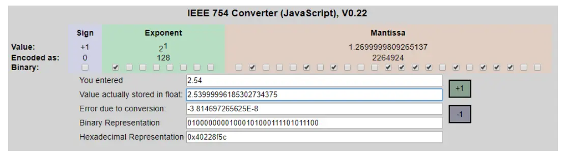
Using the last representation the value 2.54 is represented at 32 bits as: 0x40228F5C
Since we have 16-bit registers available, the value must be divided into MSW and LSW: 0x4022 (16418 decimal) are the 16 most significant bits (MSW) while 0x8F5C (36700 decimal) are the 16 least significant bits (LSW).
8.8. T-203PM-MU: MODBUS 4X HOLDING REGISTERS TABLE (FUNCTION CODE 3)
| ADDRESS (4x) | OFFSET | REGISTER | DESCRIPTION | W/R | TYPE | |
| 40001 | 0 | RESERVED | UNSIGNED 16 BIT | |||
| 40002 | 1 | ROM_FWREV | Device firmware revision | UNSIGNED 16 BIT | ||
| 40003 | 2 | USR_SLAVEID | Device slave ID | RW* | UNSIGNED 16 BIT | |
| 40004 | 3 | RESERVED | RO | UNSIGNED 16 BIT | ||
| 40005 | 4 | COMMAND | Register for command execution: REBOOT=49568 WRITE TO FLASH=49600 CLEAR ENERGIES=45505 CLEAR MIN/MAX=49612 ENABLE WRITE CUSTOM ENERGIES=49616 WRITE CUSTOM ENERGIES AND REBOOT=49617 | RO | UNSIGNED 16 BIT | |
| 40072 | 71 | USR_MULTV | MSW | Multiplier for voltage [> 0] | RW* | FLOAT 32 BIT |
| 40073 | 72 | LSW | ||||
| 40074 | 73 | USR_MULTI | MSW | Multiplier for current [> 0] | RW* | FLOAT 32 BIT |
| 40075 | 74 | LSW | ||||
| 40076 | 75 | USR_TVRATIO | MSW | Voltage transformation ratio [> 0] | RW* | FLOAT 32 BIT |
| 40077 | 76 | LSW | ||||
| 40078 | 77 | USR_AMPCUTOFF | MSW | current cutoff, 0 = disabled [A] | RW* | FLOAT 32 BIT |
| 40079 | 78 | LSW | ||||
| 40080 | 79 | USR_VOLTCUTOFF | MSW | voltage cutoff, 0 = disabled [V] | RW* | FLOAT 32 BIT |
| 40081 | 80 | LSW | ||||
| 40082 | 81 | USR_STOPBIT_PARITY_BAUDRATE | Bit [12] NR StopBit 0 = 1 stop bit 1 = 2 stop bit Bit [8-9] Parity 0=UART_PARITY_NONE 1=UART_PARITY_EVEN 2=UART_PARITY_ODD Bit [0-7] LSB Baudrate: 0=2400 1=4800 2=9600 3=19200 4=38400 5=57600 6=115200 | RW* | UNSIGNED 16 BIT |
| 40083 | 82 | USR_MEASURE | Selects the type of measure (0=AC or 1=DC) | RW* | UNSIGNED 16 BIT | ||||
|
40084 |
83 |
USR_ALARMTYPE_AO DO | Measure associated with the analog output AO (8 Bit MSB) and digital DO (8 Bit LSB). The selectable measures are: 0=NONE 1=VOLTAGE 2=CURRENT 3=ACTIVE P. 4=REACTIVE P. 5=APPARENT P. 6=FREQUENCY 7=PF 8=THD |
RW* |
NSIGNED 16 BIT | ||||
| 40085 | 84 | USR_ALARM_DO_BEHAVIOUR | Type of DO ALARMS: 0=NONE 1=MAX 2=MIN 3=INSIDE WINDOW 4=OUTSIDE WINDOW Pulses (PLS): 5=1000 PLS/kWh 6=100 PLS/kWh 7=10 PLS/kWh 8= 1 PLS/kWh 9=100 PLS/MWh 10=10 PLS/MWh 11=1 PLS/MWh | RW* | UNSIGNED 16 BIT | ||||
| 40086 | 85 | USR_AO_STARTINSCALE | MSW | Analog output: initial value of the input [V, A, W, VAR, VA, Hz, PF, THD] | RW* | FLOAT 32 BIT | |||
| 40087 | 86 | LSW | |||||||
| 40088 | 87 | USR_AO_STOPINSCALE | MSW | Analog output: final value of the input [V, A, W, VAR, VA, Hz, PF, THD] | RW* | FLOAT 32 BIT | |||
| 40089 | 88 | LSW | |||||||
| 40090 | 89 | USR_AO_STARTVOLTOUT | MSW | Analog output: minimum voltage [V] | RW* | FLOAT 32 BIT | |||
| 40091 | 90 | LSW | |||||||
| 40092 | 91 | USR_AO_STOPVOLTOUT | MSW | Analog output: maximum voltage [V] | RW* | FLOAT 32 BIT | |||
| 40093 | 92 | LSW | |||||||
| 40094 | 93 | USRRO_AO_OUTPUTVOLTAGE | MSW | Analog output: voltage generated at the output [V] | RO | FLOAT 32 BIT | |||
| 40095 | 94 | LSW | |||||||
| 40096 | 95 | USR_DO_ALNORMALLYHIGH | Digital output: alarm state, 1 = normally high 0 = normally low | RW* | UNSIGNED 16 BIT | ||||
| 40097 | 96 | USR_DO_LOWVAL | MSW | Digital output: lower alarm threshold [V, A, W, VAR, VA, Hz, PF, THD] | RW* | FLOAT 32 BIT | |||
| 40098 | 97 | LSW | |||||||
| 40099 | 98 | USR_DO_HIGHVAL | MSW | Digital output: upper alarm threshold [V, A, W, VAR, VA, Hz, PF, THD] | RW* | FLOAT 32 BIT | |||
| 40100 | 99 | LSW | |||||||
| 40101 | 100 | USR_DO_HIST | MSW | Digital output: alarm hysteresis value [V, A, W, VAR, VA, Hz, PF, THD] | RW* | FLOAT 32 BIT | |||
| 40102 | 101 | LSW | |||||||
| 40103 | 102 | USR_DO_TIMER10MS | Digital output: time filter applied to the alarm (multiples of 10ms) | RW* | UNSIGNED 16 BIT | ||||
| ALL RIGHTS RESERVED. NO PART OF THISPUBLICATION MAY BE REPRODUCED WITHOUT www.seneca.it PRIOR PERMISSION. | MI00571-1-EN | Page 21 | |||||||
| 40104 | 103 | USRRO_DO_ALSTATUS | Digital output: alarm status. 0=NONE 1=MAX_PREALARM 2=MIN_PREALARM 4=INTWIN_PRE_ALARM 8=EXTWIN_PRE_ALARM 256=MAX_ALARM 512=MIN_ALARM 1024=INTWIN_ALARM 2048=EXTWIN_ALARM |
RO |
UNSIGNED 16 BIT | |
| 40105 | 104 | MISRMS_F_V | MSW | RMS voltage measurement [V] | RO | FLOAT 32 BIT |
| 40106 | 105 | LSW | ||||
| 40107 | 106 | MISRMS_F_I | MSW | RMS current measurement [A] | RO | FLOAT 32 BIT |
| 40108 | 107 | LSW | ||||
| 40109 | 108 | MISPOW_F_ACTIVE | MSW | Active power measurement [W] | RO | FLOAT 32 BIT |
| 40110 | 109 | LSW | ||||
| 40111 | 110 | MISPOW_F_REACTIVE | MSW | Reactive power measurement [VAR] | RO | FLOAT 32 BIT |
| 40112 | 111 | LSW | ||||
| 40113 | 112 | MISPOW_F_APPARENT | MSW | Apparent power measurement [VA] | RO | FLOAT 32 BIT |
| 40114 | 113 | LSW | ||||
| 40115 | 114 | MISEN_F_ACTIVE | MSW | Active energy measurement [Wh] | RO | FLOAT 32 BIT |
| 40116 | 115 | LSW | ||||
| 40117 | 116 | MISEN_F_REACTIVE | MSW | Reactive energy measurement [VARh] | RO | FLOAT 32 BIT |
| 40118 | 117 | LSW | ||||
| 40119 | 118 | MISEN_F_APPARENT | MSW | Apparent energy measurement [VAh] | RO | FLOAT 32 BIT |
| 40120 | 119 | LSW | ||||
| 40121 | 120 | MISFREQ_F | MSW | Frequency measurement [Hz] | RO | FLOAT 32 BIT |
| 40122 | 121 | LSW | ||||
| 40123 | 122 | MISPF_F | MSW | PF measurement PF (±0..1) | RO | FLOAT 32 BIT |
| 40124 | 123 | LSW | ||||
| 40125 | 124 | MISTHD_F | MSW | THD measurement (0..100%) | RO | FLOAT 32 BIT |
| 40126 | 125 | LSW | ||||
| 40127 | 126 | RESERVED | UNSIGNED 32 BIT | |||
| 40128 | 127 | |||||
| 40129 | 128 | RESERVED | UNSIGNED 16 BIT | |||
| 40130 | 129 | RESERVED | FLOAT 32 BIT | |||
| 40131 | 130 | |||||
| 40132 | 131 | RESERVED | FLOAT 32 BIT | |||
| 40133 | 132 | |||||
| 40134 | 133 | RESERVED | FLOAT 32 BIT | |||
| 40135 | 134 | |||||
| 40136 | 135 | RESERVED | FLOAT 32 BIT |
| 40137 | 136 | |||||
| 40138 | 137 | RESERVED | FLOAT 32 BIT | |||
| 40139 | 138 | |||||
| 40140 | 139 | MIN_MISRMS_F_V | MSW | Minimum RMS voltage measurement [V] | RO | FLOAT 32 BIT |
| 40141 | 140 | LSW | ||||
| 40142 | 141 | MAX_MISRMS_F_V | MSW | Maximum RMS voltage measurement [V] | RO | FLOAT 32 BIT |
| 40143 | 142 | LSW | ||||
| 40144 | 143 | MIN_MISRMS_F_I | MSW | Minimum RMS current measurement [A] | RO | FLOAT 32 BIT |
| 40145 | 144 | LSW | ||||
| 40146 | 145 | MAX_MISRMS_F_I | MSW | Maximum RMS current measurement [A] | RO | FLOAT 32 BIT |
| 40147 | 146 | LSW | ||||
| 40148 | 147 | MIN_MISPOW_F_ACTIVE | MSW | Minimum active power measurement [W] | RO | FLOAT 32 BIT |
| 40149 | 148 | LSW | ||||
| 40150 | 149 | MAX_MISPOW_F_ACTIVE | MSW | Maximum active power measurement [W] | RO | FLOAT 32 BIT |
| 40151 | 150 | LSW | ||||
| 40152 | 151 | MIN_MISPOW_F_REACTIVE | MSW | Minimum reactive power measurement [VAR] | RO | FLOAT 32 BIT |
| 40153 | 152 | LSW | ||||
| 40154 | 153 | MAX_MISPOW_F_REACTIVE | MSW | Maximum reactive power measurement [VAR] | RO | FLOAT 32 BIT |
| 40155 | 154 | LSW | ||||
| 40156 | 155 | MIN_MISPOW_F_APPARENT | MSW | Minimum apparent power measurement [VA] | RO | FLOAT 32 BIT |
| 40157 | 156 | LSW | ||||
| 40158 | 157 | MAX_MISPOW_F_APPARENT | MSW | Minimum apparent power measurement [VA] | RO | FLOAT 32 BIT |
| 40159 | 158 | LSW | ||||
| 40160 | 159 | MIN_MISFREQ_F | MSW | Minimum frequency measurement [Hz] | RO | FLOAT 32 BIT |
| 40161 | 160 | LSW | ||||
| 40162 | 161 | MAX_MISFREQ_F | MSW | Maximum frequency measurement [Hz] | RO | FLOAT 32 BIT |
| 40163 | 162 | LSW | ||||
| 40164 | 163 | MIN_MISPF_F | MSW | Minimum PF measurement (±0..1) | RO | FLOAT 32 BIT |
| 40165 | 164 | LSW | ||||
| 40166 | 165 | MAX_MISPF_F | MSW | Maximum PF measurement (±0..1) | RO | FLOAT 32 BIT |
| 40167 | 166 | LSW | ||||
| 40168 | 167 | MIN_MISTHD_F | MSW | Minimum THD measurement (0..100%) | RO | FLOAT 32 BIT |
| 40169 | 168 | LSW | ||||
| 40170 | 169 | MAX_MISTHD_F | MSW | Maximum THD measurement (0..100%) | RO | FLOAT 32 BIT |
| 40171 | 170 | LSW | ||||
| 40172 | 171 | RESERVED | MSW | UNSIGNED 32 BIT | ||
| 40173 | 172 | LSW |
| 40174 | 173 | MISRMS_INT_V | RMS voltage measurement [V / 10]: (Example: 2300 -> 230.0 V) | RO | SIGNED 16 BIT | ||||
| 40175 | 174 | MISRMS_INT_I | RMS current measurement [A/10]: (Example: 1000 -> 100.0 A) | RO | SIGNED 16 BIT | ||||
| 40176 | 175 | MISPOW_INT_ACTIVE | MSW | Active power measurement [W/10]: (Example 1000 -> 100.0 W) | RO | SIGNED 32 BIT | |||
| 40177 | 176 | LSW | |||||||
| 40178 | 177 | MISPOW_INT_REACTIVE | MSW | Reactive power measurement [VAR/10]: (Example 1000 -> 100.0 VAR) | RO | SIGNED 32 BIT | |||
| 40179 | 178 | LSW | |||||||
| 40180 | 179 | MISPOW_INT_APPARENT | MSW | Apparent power measurement [VA/10]: (Example 1000 -> 100.0 VA) | RO | SIGNED 32 BIT | |||
| 40181 | 180 | LSW | |||||||
| 40182 | 181 | EN_INT_ACTIVE | MMSW | Active energy measurement [Wh/10]: (Example 1000 -> 100.0 Wh) | RW** | UNSIGNED 64 BIT | |||
| 40183 | 182 | MSW | |||||||
| 40184 | 183 | LSW | |||||||
| 40185 | 184 | LLSW | |||||||
| 40186 | 185 | EN_INT_REACTIVE | MMSW | Reactive energy measurement [VARh/10]: (Example 1000 -> 100.0 VARh) | RW** | UNSIGNED 64 BIT | |||
| 40187 | 186 | MSW | |||||||
| 40188 | 187 | LSW | |||||||
| 40189 | 188 | LLSW | |||||||
| 40190 | 189 | EN_INT_APPARENT | MMSW | Apparent energy measurement [VAh/10]: (Example 1000 -> 100.0 VAh) | RW** | UNSIGNED 64 BIT | |||
| 40191 | 190 | MSW | |||||||
| 40192 | 191 | LSW | |||||||
| 40193 | 192 | LLSW | |||||||
| 40194 | 193 | MIS_INT_FREQ | Frequency measurement [Hz/10]: (Example 500 -> 50.0 Hz) | RO | UNSIGNED 16 BIT | ||||
| 40195 | 194 | MIS_INT_PF | PF measurement [±0..1000]: (Example 755 -> 0.755) | RO | SIGNED 16 BIT | ||||
| 40196 | 195 | MIS_INT_THD | THD measurement [0..100% / 10]: (Example 800 -> 80%) | RO | SIGNED 16 BIT | ||||
| 40197 | 196 | MIN_MISRMS_INT_V | Minimum RMS voltage measurement [V/10]: (Example 2300 -> 230.0 V) | RO | SIGNED 16 BIT | ||||
| 40198 | 197 | MAX_MISRMS_INT_V | Maximum RMS voltage measurement [V/10]: (Example 2300 -> 230.0 V) | RO | SIGNED 16 BIT | ||||
| 40199 | 198 | MIN_MISRMS_INT_I | Minimum RMS current measurement [A/10]: (Example 1000 -> 100.0 A) | RO | SIGNED 16 BIT | ||||
| 40200 | 199 | MAX_MISRMS_INT_I | Maximum RMS current measurement [A/10]: (Example 1000 -> 100.0 A) | RO | SIGNED 16 BIT | ||||
| 40201 | 200 | MIN_MISPOW_INT_ACTIVE | MSW | Minimum active power | RO | SIGNED 32 BIT | |||
| ALL RIGHTS RESERVED. NO PART OF THIS PUBLICATION MAY BE REPRODUCED WITHOUT www.seneca.it PRIOR PERMISSION. | MI00571-1-EN | Page 24 | |||||||
| 40202 | 201 | LSW | measurement [W/10]: (Example 1000 -> 100.0 W) | |||
| 40203 | 202 | MAX_MISPOW_INT_ACTIVE | MSW | Maximum active power measurement [W/10]: (Example 1000 -> 100.0 W) | RO | SIGNED 32 BIT |
| 40204 | 203 | LSW | ||||
| 40205 | 204 | MIN_MISPOW_INT_REACTIVE | MSW | Minimum reactive power measurement [VAR/10]: (Example 1000 -> 100.0 VAR) | RO | SIGNED 32 BIT |
| 40206 | 205 | LSW | ||||
| 40207 | 206 | MAX_MISPOW_INT_REACTIVE | MSW | Maximum reactive power measurement [VAR/10]: (Example 1000 -> 100.0 VAR) | RO | SIGNED 32 BIT |
| 40208 | 207 | LSW | ||||
| 40209 | 208 | MIN_MISPOW_INT_APPARENT | MSW | Minimum apparent power measurement [VA/10]: (Example 1000 -> 100.0 VA) | RO | SIGNED 32 BIT |
| 40210 | 209 | LSW | ||||
| 40211 | 210 | MAX_MISPOW_INT_APPARENT | MSW | Maximum apparent power measurement [VA/10]: (Example 1000 -> 100.0 VA) | RO | SIGNED 32 BIT |
| 40212 | 211 | LSW | ||||
| 40213 | 212 | MIN_MIS_INT_FREQ | Minimum frequency measurement [Hz/10]: (Example 500 -> 50.0 Hz) | RO | SIGNED 16 BIT | |
| 40214 | 213 | MAX_MIS_INT_FREQ | Maximum frequency measurement [Hz/10]: (Example 500 -> 50.0 Hz) | RO | SIGNED 16 BIT | |
| 40215 | 214 | MIN_MIS_INT_PF | Minimum PF measurement [±0..1000]: (Example 755 -> 0.755) | RO | SIGNED 16 BIT | |
| 40216 | 215 | MAX_MIS_INT_PF | Maximum PF measurement [±0..1000]: (Example 755 -> 0.755) | RO | SIGNED 16 BIT | |
| 40217 | 216 | MIN_MIS_INT_THD | Minimum THD/10 measurement (0..100%): (Example 800 -> 80.0%) | RO | SIGNED 16 BIT | |
| 40218 | 217 | MAX_MIS_INT_THD | Maximum THD/10 measurement (0..100%): (Example 800 -> 80.0%) | RO | SIGNED 16 BIT |
By adding offset 1000 to the register it is possible to obtain the 32-bit swapped values, for example the floating point current measurement register:
| 40107 | 106 | MISRMS_F_I | MSW | Current measurement RMS [A] | RO | FLOAT 32 BIT |
| 40108 | 107 | LSW |
The same register can also be found at 41107-41108 swapped:
| 41107 | 1106 | MISRMS_F_I | LSW | Current measurement RMS [A] | RO | FLOAT 32 BIT |
| 41108 | 1107 | MSW |
ALL RIGHTS RESERVED. NO PART OF THIS PUBLICATION MAY BE REPRODUCED WITHOUT PRIOR PERMISSION.
![]() www.seneca.it
www.seneca.it
MI00571-1-EN
![]()
[email protected]
+52(33)-3823-4349


