![]()
TMD2635 Low Power Proximity Detection
User Manual
Application Note
AN000646
Minimizing Power Consumption with the TMD2635, TMD2636 and TMD2637
Introduction
![]() Information
Information
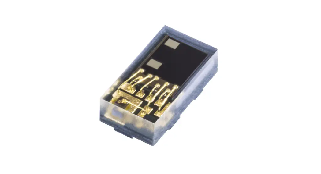
This document applies to the arms TMD2635, TMD2636, and TMD2637 devices. References to these devices will be abbreviated to “TMD2635/6/7” throughout.
The ams TMD2635/6/7 was developed for proximity sensing applications requiring small size, low power, and short-range operation. Example applications include battery-powered wearable products such as true wireless stereo earbuds, glasses, watches, etc.
Low power system designers need to strike a balance between competing requirements for optimal performance and minimal power consumption. The TMD2635/6/7 offers features that support low power operation but the application’s required proximity response will ultimately limit the degree to which these features can be leveraged. This application note will describe the settings of the TMD2635/6/7 that affect power consumption and demonstrate how to calculate power consumption based on the sensor’s configuration.
![]() Information
Information
For guidance on optimizing the sensor’s proximity response, refer to as application note AN000556 “Proximity Detection – Optimizing Proximity Parameters.”
Configuring the TMD2635/6/7 for low power operation requires an understanding of current consumed during all operating states and how to control the duration of those states. Knowing these two things, the “duty cycle” of the sensor can be adjusted. Duty cycle is defined as the fraction of one operating period in which the sensor is active; therefore a “low” duty cycle means that the sensor spends most of its time in a low power state. Ideally, the sensor should operate at full power only as long as is necessary to meet the application’s proximity response requirements.
Duty cycle control of the TMD2635/6/7 can be achieved in a couple of ways. The first and most basic is through the configuration of the sensor’s proximity cycle timing.
Proximity Cycle Timing & States
When the TMD2635/6/7is fully operating, it loops in a ‘proximity cycle’ whose timing is controlled by configuration register settings. A single proximity sample (Figure 1) consists of multiple user-programmable pulses (quantity “n”) which enable the IR light source (emitter) when high. In the case of the TMD2635/6/7, the IR emitter is called a “vertical-cavity surface-emitting laser” (VCSEL) and the IR detector is a photodiode. PRATE is the duration of the entire proximity sample.
Figure 1: Pulse Timing for a Single proximity Sample
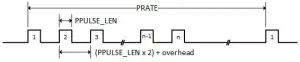
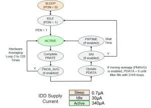
The proximity cycle state diagram (Figure 2) shows the sequence of operation and denotes the average amount of IDD current consumed during each state. The proximity ample pulsing shown above occurs entirely during the ACTIVE state. This state consumes the most power by far, drawing over 11× more average IDD current than IDLE states and 485× more than the SLEEP state.
IDD current is sourced from a 1.8 V supply and is consumed by the TMD2635/6/7’s digital circuitry.
During the ACTIVE state only, there is another current that is consumed by the TMD2635/6/7’s VCSEL IR emitter. This current is sourced from a VCSEL-dedicated 3.3 V supply and flows only during the high time of each drive pulse. The average value of this current is in the 3.5–15 mA¹ range. Although the drive pulses are narrow, the VCSEL becomes a more significant power consumer as the number and the width of these pulses increase. It is important that the 3.3 V power supply is capable of supporting pulses up to 15 mA in amplitude and 32 µs in duration.
IDD and VCSEL current combine during the ACTIVE state to create a major portion of the sensor’s overall power load to the system. Pulse length and the number of pulses should be minimized when configuring the sensor for the required proximity response.
¹VCSEL drive current is factory-trimmed to achieve a specific proximity response at a given PLDRIVE setting. The actual drive current can be as much as ± 50% of the value listed in the PLDRIVE bit field. This means the nominal 7–10 mA range can actually be 3.5–15 mA.
Figure 2: Proximity Cycle Simplified State Diagram
Configuration Register Settings
There is a specific set of register settings that directly affect both the timing and the power consumption of the proximity cycle.
The following bit fields configure the pulse train of a single proximity sample:
- PULSE (number of pulses, 1–64). Power consumption is directly proportional to the number of pulses.
- PPULSE_LEN (pulse length, 1–32 µs). Power consumption is directly proportional to the pulse length.
- PRATE (proximity sample duration, 88–22528 µs). Longer PRATE can reduce power consumption by decreasing the duty cycle of the proximity loop.
The following bit fields add optional wait time between proximity samples:
- PW TIMES (proximity wait time, 2.78–712 ms). Longer wait times can reduce power consumption by decreasing the duty cycle of the proximity loop.
- PWLONG (wait time 12× extension, 33.36–8544 ms). Longer wait times can reduce power consumption by decreasing the duty cycle of the proximity loop.
The following bit field averages multiple proximity samples into a single result:
- PROX_AVG (hardware averaging, 2–128 samples). Power consumption is directly proportional to the number of hardware averaging repetitions.
Note that the PMAVG bit field (proximity moving average, 2, 4, or 8 values) adds delay only at loop start-up and thereafter it has no effect on duty cycle or power consumption.
Although the following bit field does not affect loop timing, it does affect power consumption:
- PLDRIVE (VCSEL drive current, 7–10 mA). Power consumption is directly proportional to VCSEL drive strength
Once the optimal proximity response has been established, potential power savings can be explored by experimenting with reductions in duty cycle and drive current.
Application Software Control
The second level of duty cycle control exists at the application software level. The host processor can be programmed to cycle the sensor’s active/inactive states in either a “polled” or an “interrupt-driven” fashion.
A polling cycle consists of waking up the sensor, sampling data then putting the sensor back to sleep.
An interrupt-driven cycle consists of waking up the sensor, reading its previous sample then letting it free-run. When the next data event occurs, the sensor signals an interrupt to the host and automatically goes into a low power state.
The interrupt cycle described above employs the TMD2635/6/7 “Sleep after Interrupt” (SAI) feature. Referring to Figure 2, when the IDLE state is entered following an SAI-enabled interrupt, the oscillator is deactivated to reduce power consumption. The device can only be reactivated by clearing interrupt flags in the STATUS register.
TMD2635/6/7 interrupt events are programmable. Refer to the latest datasheets for a description of the following features that configure interrupt trigger conditions:
- Proximity High and Low Thresholds – Generate an interrupt when PDATA falls outside of the threshold range and the persistence filter value is reached. See the PILTL, PILTH, PIHTL, and PIHTH register descriptions in the TMD2635/6/7 datasheets.
- Persistence Filter – Counts consecutive occurrences of PDATA values that fall outside of the threshold range. See the PERS register description in the TMD2635/6/7 datasheets.
- Proximity Interrupt Mode (PIM) – Qualifies interrupt assertion based on the threshold crossing’s level or state change. See the INTENAB register description and Figure 43 in the TMD2635/6/7 datasheets.
Timing in the interrupt-driven scenario is less deterministic than in a polled scenario. Event-driven duty cycles depend on host response time and the changing stimulus in the sensor’s field of view that trigger interrupts based on the register configuration described above. This timing variability makes accurate power calculation difficult unless simplifying assumptions are made. Bench characterization is the best way to accurately assess power consumption under such dynamic conditions.
Assuming that the host will service interrupts promptly, the sensor will spend a majority of its time in states that draw idle current (30 µA average) while free-running, waiting for the next interrupt trigger event to drive it into a low power state. This interrupt-driven approach will not be able to conserve power as well as a polled design that purposely maximizes the time spent in SLEEP state drawing 0.7 µA average current.
Power Calculation Examples
Proximity Cycle Power Calculations
The TMD2635/6/7 datasheets provide all of the information needed to calculate the average current consumed during the sensor’s proximity cycle. For example, consider a sensor configured as follows:
Figure 3: Device Configuration Proximity Cycle
| Device Configuration | Inputs | Units | Range. Notes |
| VDD3 Voltage | 3.0 | V | 2.9 V to 3.6 V |
| VDD Voltage | 2. | V | 1.7 Vto2.0V |
| IDD Current SLEEP state | 0.7 | µA | SLEEP state occurs when PON = 0 and PC bus Is idle. If SLEEP state has been entered as the result of operational flow. SAI = 1 and PON will remain high. |
| IDD Current IDLE state | 30 | µA | The IDLE state occurs when PON = 1 and the device Is not in the ACTIVE state. |
| IDD Current ACTIVE state | 340 | µA | The ACTIVE state occurs when PON = 1 and the device is actively integrating. |
| VCSEL Current (PLDRIVE) | 7 | mA | 7 mA to 10 mA |
| Number of Pulses (PULSE) | 4 | x | 1 to 64 |
| Pulse Length (PPULSE_LEN) | 16 | µs | 1/2/4/8/12/16/24/32 ps |
| Wait Time (PWTIME) | 2780 | µs | 2.78 ms to 712 ms or 33.36 ms to 8544 ms when PWLONG=1, ((PVVTIME=0..255)+1)*2.78 ms |
| PRATE | 2816 | µs | 88 ps to 22528 ps, ((PRATE=0..255)+1)*88 ps, If PRATE is programmed to a value that is less than the time required for the selected number of pulses, then it is ignored and the proximity cycle duration is extended to allow for the full number of pulses programmed. |
| Hardware Averaging (PROX_AVG) | 1 | x | 1/2/4/8/16/32/64/128 (set to 1 if disabled) |
Based on the sensor configuration above, duty cycle time calculations can be made.
Figure 4: Loop Calculations Proximity Cycle
| Per Loop Time Calculations | Outputs | Units | Formula |
| Active Time per Proximity Cycle | 406.75 | µs | = (7 x PPULSE_LEN) + (PPULSE x ((2 x PPULSE_LEN) + 22 ps)) + 78.75 ps |
| Total Active Time per Loop | 406.75 | µs | = (Active Time per Proximity Cycle) x (PROX_AVG) |
| Idle Time (all-time except active) | 5189.25 | µs | = (PVVTIME) + [If PRATE > (Active Time per Proximity Cycle), then ((PRATE — (Active Time per Proximity Cycle)) x (PROX_AVG)), else 0] |
| Total Loop Time | 5596 | µs | = (Total Active Time per Loop) + (Idle Time) |
Applying the duty cycle time calculations above to the appropriate power supplies will determine the average current drawn from each source.
Figure 5: Power Calculations Proximity Cycle
| Power Calculations | Outputs | Units | Formula |
| Average VCSEL Current | 80.06 | µW | = (PLDRIVE x 1000) x ((PPULSE x PPULSE_LEN x PROX_AVG) / (Total Loop Time)) |
| Average VCSEL Power | 240.17 | µW | = (Average VCSEL Current) x (VDD3 Voltage) |
| Average IDD Current | 52.53 | . µW | . = [(IDD Current ACTIVE state) x ((Total Active Time per Loop) / (Total Loop Time))] + [(IDD Current IDLE state) x ((Idle Time) / (Total Loop Time))) |
| Average IDD Power | 94.56 | µW | = (Average IDD Current) x (VDD Voltage) |
| Total Average Power Consumption | 334.73 | µW | = (Average IDD Power) + (Average VCSEL Power) |
The calculations demonstrated above are made based on the proximity cycle of the sensor while it is fully operational and free-running.
Polling Cycle Power Calculations
The following example calculates the average power consumed by a hypothetical polling cycle that consists of waking up the sensor, collecting a single data sample from 1 proximity cycle than putting the sensor back to sleep. Consider the following sensor configuration with software-controlled duty cycle timing:
Figure 6: Device Configuration Polling Cycle
| Device Configuration | Inputs | Units | Range, Notes |
| VDD3 Voltage | 3 | V | 2.9 V to 3.6 V |
| VDD Voltage | 1.8 | V | 1.7 V to 2.0 V |
| IDD Current -SLEEP state | 0.7 | µA | SLEEP state occurs when PON = 0 and PC bus Is Idle. If SLEEP state has been entered as the result of operational flow, SAI = 1 and PON will remain high. |
| IDD Current – IDLE state | 30 | µA | The IDLE state occurs when PON = 1 and the device is not in the ACTIVE state. |
| IDD Current – ACTIVE state | 340 | µA | The ACTIVE state occurs when PON = 1 and the device is actively Integrating. |
| VCSEL Current | 7 | mA | 7 mA to 10 mA |
| Number of Pulses (PULSE) | 4 | x | 1 to 64 |
| Pulse Length (PPULSE_LEN) | 16 | µs | 112/4/6/12/16/24/32 ps |
| Time Between Proximity Samples | 250 | ms | Controlled by a software routine |
| Wakeup Time | 100 | µs | |
| Time Post Active Until Sleep | 500 | µs | Controlled by a software routine |
Based on the sensor configuration above, duty cycle time calculations can be made.
Figure 7: Time Calculations Polling Cycle
| Per Loop Time Calculations | Outputs | Units | Formula |
| Active Time | 406.75 | µs | = (7 x PPULSE_LEN) + PPULSE x (2 x PPULSE_LEN + 22 μs) + 78.75 μs |
| Idle Time (wakeup + post active time) | 600 | µs | = (Wakeup Time) + (Time Post Active Until Sleep) |
| Sleep Time | 248993.3 | µs | = (Time Between Proximity Samples x 1000) – (Active Time) – (Idle Time) |
| Total Loop Time | 250000 | µs | = (Active Time) + (Idle Time) + (Sleep Time) |
In the polling cycle described above, the host interaction with the sensor generates bus activity that consumes system current through the I²C bus pull-up resistors. This power can be accounted for in the sensor’s total power calculation.
To analyze I²C bus activity, consider the following assumptions about the steps taken by the polling software routine, including the number of 9-bit bytes transferred during each transaction
- Write the ENABLE register to wake up the sensor (3 bytes)
- Wait at least (Wakeup Time + Active Time) for a proximity cycle to occur
- Read the PDATAL and PDATAH registers (5 bytes)
- Write the ENABLE register to put the sensor to sleep (3 bytes)
This short routine generates 11 bytes of bus activity.
Consider the following I²C bus parameters:
Figure 8: I²C Bus Parameters
| I²C Bus Parameters | Outputs | Units | Notes |
| I²C Bus Voltage | 1.8 | V | |
| Pull Up Resistance | 2200 | Ohms | Value-based on the I²C bus voltage, system bus speed and trace capacitance |
| I²C Bus Speed | 200000 | Hz | Assume 50% SCL duty cycle |
| Number of Bytes per Cycle | 11 |
Applying the duty cycle time calculations above to the appropriate power supplies will determine the average current drawn from each source. Using the I²C bus parameters above, bus current and power consumed during each polling cycle can be estimated.
More details on I²C read and write transactions can be found in the TMD2635/6/7 datasheets.
Figure 9: Power Calculations Polling Cycles
| Power Calculations | Outputs | Units | Formula |
| Average VCSEL Current | 1.79 | µA | = (VCSEL Current x 1000) x (PPULSE x PPULSE_LEN) /(Total Loop Time) |
| Average VCSEL Power | 5.38 | µW | = (Average VCSEL Current) x (VDD3 Voltage) |
| Average IDD Current | 1.32 | µA | = (IDD Current ACTIVE State) x (Active Time / Total Loop Time) + (IDD Current SLEEP State) x (Sleep Time / Total Loop Time) + (IDD Current IDLE State) x (Idle Time / Total Loop Time) |
| Average IDD Power | 2.38 | µW | = (Average IDD Current) x (VDD Voltage) |
| I²C Bus Curren per Polling Cycle (1) | 0.41 | µA | = [(( Bus Voltage) / (Pull up resistance)) x 1e6] x [((Number of Bytes per Cycle) x (9 bits per Byte)) x (1 / (Bus Speed))] |
| I²C Bus Power per Polling Cycle | 0.73 | µW | = (I²C Bus Current per Polling Cycle) x ( Bus Voltage) |
| Total Power Consumption | 8.49 | µW | = (Average VCSEL Power) + (Average IDD Power) + (I²C Bus Power) |
Using the full bit period in the current calculation accounts for both the SCL and SDA lines assuming that they both maintain a 50% duty cycle and that half of the data bits are low during each bus transaction. Actual bus power will vary with data value
Summary
Implementing proximity detection in a low-power system should begin by optimizing the sensor response according to the system detect/release requirements. Power savings can then be explored by experimenting with changes in the proximity cycle timing, emitter drives current, and duty cycling at the application software level. A polled sensor design will provide more predictable duty cycle control that can achieve lower average power consumption than an interrupt-driven approach. Calculation of TMD2635/6/7 average power consumption can be made using the techniques outlined in this document.
References
![]() For further information, please refer to the following documents:
For further information, please refer to the following documents:
- TMD2635 Datasheet
- TMD2636 Datasheet
- TMD2637 Datasheet
- AN000556 Proximity Detection – Optimizing Proximity Parameters
Revision Information
| Changes from previous version to current revision v3-00 | Page |
| Changed TMD2635/6 to TMD2635/6/7 | 3,4,7,8,11,13 |
| Added TMD2637 datasheet to References | 14 |
- Page and figure numbers for the previous version may differ from page and figure numbers in the current revision.
- Correction of typographical errors is not explicitly mentioned.
Legal Information
Copyrights & Disclaimer
Copyright ams AG, Tobelbader Strasse 30, 8141 Premstaetten, Austria-Europe. Trademarks Registered. All rights reserved.
The material herein may not be reproduced, adapted, merged, translated, stored, or used without the prior written consent of the copyright owner.
Information in this document is believed to be accurate and reliable. However, ams AG does not give any representations or warranties, expressed or implied, as to the accuracy or completeness of such information and shall have no liability for the consequences of use of such information.
Applications that are described herein are for illustrative purposes only. ams AG makes no representation or warranty that such applications will be appropriate for the specified use without further testing or modification. ams AG takes no responsibility for the design, operation and testing of the applications and end-products as well as assistance with the applications or end-product designs when using ams AG products. ams AG is not liable for the suitability and fit of ams AG products in applications and end-products planned.
ams AG shall not be liable to recipient or any third party for any damages, including but not limited to personal injury, property damage, loss of profits, loss of use, interruption of business or indirect, special, incidental or consequential damages, of any kind, in connection with or arising out of the furnishing, performance or use of the technical data or applications described herein. No obligation or liability to recipient or any third party shall arise or flow out of ams AG rendering of technical or other services.
ams AG reserves the right to change information in this document at any time and without notice.
RoHS Compliant & ams Green Statement
RoHS Compliant: The term RoHS compliant means that ams AG products fully comply with current RoHS directives. Our semiconductor products do not contain any chemicals for all 6 substance categories plus additional 4 substance categories (per amendment EU 2015/863), including the requirement that lead not exceed 0.1% by weight in homogeneous materials. Where designed to be soldered at high temperatures, RoHS compliant products are suitable for use in specified lead-free processes.
ams Green (RoHS compliant and no Sb/Br/Cl): ams Green defines that in addition to RoHS compliance, our products are free of Bromine (Br) and Antimony (Sb) based flame retardants (Br or Sb do not exceed 0.1% by weight in homogeneous material) and do not contain Chlorine (Cl does not exceed 0.1% by weight in homogeneous material).
Important Information: The information provided in this statement represents ams AG’s knowledge and belief as of the date that it is provided. AMS AG bases its knowledge and belief on information provided by third parties and makes no representation or warranty as to the accuracy of such information. Efforts are underway to better integrate information from third parties. ams AG has taken and continues to take reasonable steps to provide representative and accurate information but may not have conducted destructive testing or chemical analysis on incoming materials and chemicals. ams AG and ams AG suppliers consider certain information to be proprietary, and thus CAS numbers and other limited information may not be available for release.
Headquarters
ams AG
Tobelbader Strasse 30
8141 Premstaetten
Austria, Europe
Tel: +43 (0) 3136 500 0
Please visit our website at www.ams.com
Buy our products or get free samples online at www.ams.com/Products
Technical Support is available at www.ams.com/Technical-Support
Provide feedback about this document at www.ams.com/Document-Feedback
For sales offices, distributors and representatives go to www.ams.com/Contact
For further information and requests, e-mail us at [email protected]
Application Note • PUBLIC
AN000646 • v3-00 • 2021-Mar-26


