
F-Tile JESD204C Intel FPGA IP Design Example
About the F-Tile JESD204C Intel® FPGA IP Design Example User Guide
This user guide provides the features, usage guidelines, and detailed description about the design examples for the F-Tile JESD204C Intel® FPGA IP using Intel Agilex™ devices.
Intended Audience
This document is intended for:
- Design architect to make IP selection during system level design planning phase
- Hardware designers when integrating the IP into their system level design
- Validation engineers during system level simulation and hardware validation phase
Related Documents
The following table lists other reference documents which are related to the F-Tile JESD204C Intel FPGA IP.
Table 1. Related Documents
| Reference | Description |
| F-Tile JESD204C Intel FPGA IP User Guide | Provides information about the F-Tile JESD204C Intel FPGA IP. |
| F-Tile JESD204C Intel FPGA IP Release Notes | Lists the changes made for the F-Tile JESD204C F-Tile JESD204C in a particular release. |
| Intel Agilex Device Data Sheet | This document describes the electrical characteristics, switching characteristics, configuration specifications, and timing for Intel Agilex devices. |
Acronyms and Glossary
Table 2. Acronym List
| Acronym | Expansion |
| LEMC | Local Extended Multiblock Clock |
| FC | Frame clock rate |
| ADC | Analog to Digital Converter |
| DAC | Digital to Analog Converter |
| DSP | Digital Signal Processor |
| TX | Transmitter |
| RX | Receiver |
| Acronym | Expansion |
| DLL | Data link layer |
| CSR | Control and status register |
| CRU | Clock and Reset Unit |
| ISR | Interrupt Service Routine |
| FIFO | First-In-First-Out |
| SERDES | Serializer Deserializer |
| ECC | Error Correcting Code |
| FEC | Forward Error Correction |
| SERR | Single Error Detection (in ECC, correctable) |
| DERR | Double Error Detection (in ECC, fatal) |
| PRBS | Pseudorandom binary sequence |
| MAC | Media Access Controller. MAC includes protocol sublayer, transport layer, and data link layer. |
| PHY | Physical Layer. PHY typically includes the physical layer, SERDES, drivers, receivers and CDR. |
| PCS | Physical Coding Sub-layer |
| PMA | Physical Medium Attachment |
| RBD | RX Buffer Delay |
| UI | Unit Interval = duration of serial bit |
| RBD count | RX Buffer Delay latest lane arrival |
| RBD offset | RX Buffer Delay release opportunity |
| SH | Sync header |
| TL | Transport layer |
| EMIB | Embedded Multi-die Interconnect Bridge |
Table 3. Glossary List
| Term | Description |
| Converter Device | ADC or DAC converter |
| Logic Device | FPGA or ASIC |
| Octet | A group of 8 bits, serving as input to 64/66 encoder and output from the decoder |
| Nibble | A set of 4 bits which is the base working unit of JESD204C specifications |
| Block | A 66-bit symbol generated by the 64/66 encoding scheme |
| Line Rate | Effective data rate of serial link Lane Line Rate = (Mx Sx N’x 66/64 x FC) / L |
| Link Clock | Link Clock = Lane Line Rate/66. |
| Frame | A set of consecutive octets in which the position of each octet can be identified by reference to a frame alignment signal. |
| Frame Clock | A system clock which runs at the frame’s rate, that must be 1x and 2x link clock. |
| Term | Description |
| Samples per frame clock | Samples per clock, the total samples in frame clock for the converter device. |
| LEMC | Internal clock used to align the boundary of the extended multiblock between lanes and into the external references (SYSREF or Subclass 1). |
| Subclass 0 | No support for deterministic latency. Data should be immediately released upon lane to lane deskew on receiver. |
| Subclass 1 | Deterministic latency using SYSREF. |
| Multipoint Link | Inter-device links with 2 or more converter devices. |
| 64B/66B Encoding | Line code that maps 64-bit data to 66 bits to form a block. The base level data structure is a block that starts with 2-bit sync header. |
Table 4. Symbols
| Term | Description |
| L | Number of lanes per converter device |
| M | Number of converters per device |
| F | Number of octets per frame on a single lane |
| S | Number of samples transmitted per single converter per frame cycle |
| N | Converter resolution |
| N’ | Total number of bits per sample in the user data format |
| CS | Number of control bits per conversion sample |
| CF | Number of control words per frame clock period per link |
| HD | High Density user data format |
| E | Number of multiblock in an extended multiblock |
F-Tile JESD204C Intel FPGA IP Design Example Quick Start Guide
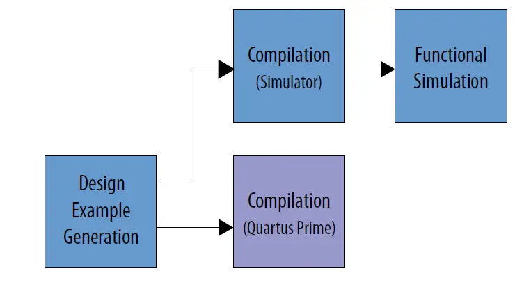
The F-Tile JESD204C Intel FPGA IP design examples for Intel Agilex devices features a simulating testbench and a hardware design that supports compilation and hardware testing.
You can generate the F-Tile JESD204C design examples through the IP catalog in the Intel Quartus® Prime Pro Edition software.
Figure 1. Development Stages for the Design Example
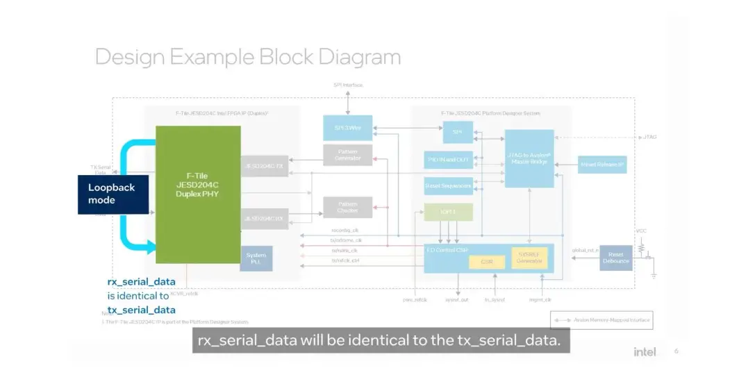
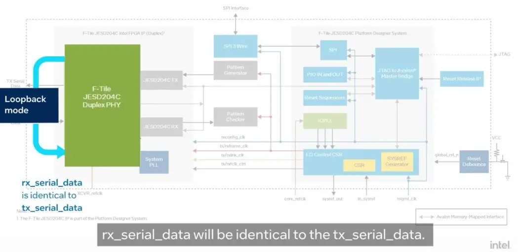
Design Example Block Diagram
Figure 2. F-Tile JESD204C Design Example High-level Block Diagram
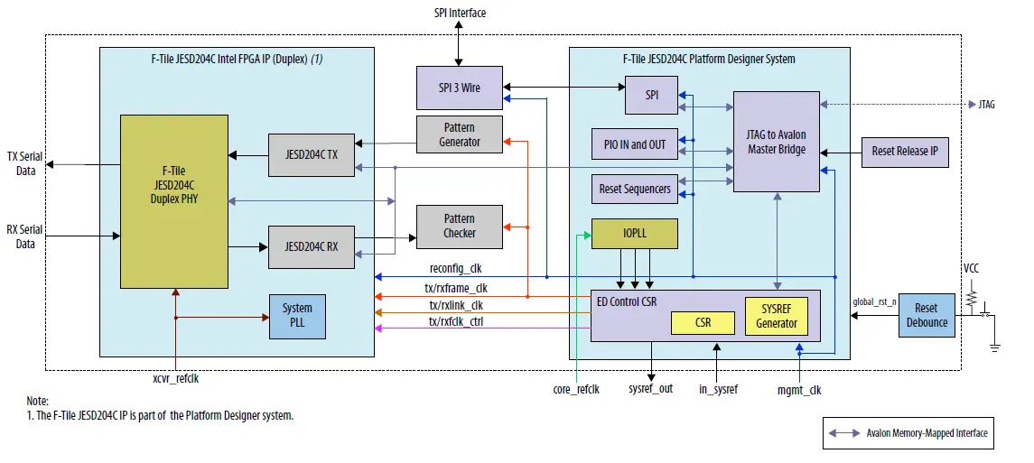
The design example consists of the following modules:
- Platform Designer system
- F-Tile JESD204C Intel FPGA IP
- JTAG to Avalon Master bridge
- Parallel I/O (PIO) controller
- Serial Port Interface (SPI)—master module— IOPLL
- SYSREF generator
- Example Design (ED) Control CSR
- Reset sequencers
- System PLL
- Pattern generator
- Pattern checker
Table 5. Design Example Modules
| Components | Description |
| Platform Designer system | The Platform Designer system instantiates the F-Tile JESD204C IP data path and supporting peripherals. |
| F-Tile JESD204C Intel FPGA IP | This Platform Designer subsystem contains the TX and RX F-Tile JESD204C IPs instantiated together with the duplex PHY. |
| JTAG to Avalon Master bridge | This bridge provides system console host access to the memory-mapped IP in the design through the JTAG interface. |
| Parallel I/O (PIO) controller | This controller provides a memory-mapped interface for sampling and driving general purpose I/O ports. |
| SPI master | This module handles the serial transfer of configuration data to the SPI interface on the converter end. |
| SYSREF generator | The SYSREF generator uses the link clock as a reference clock and generates SYSREF pulses for the F-Tile JESD204C IP. Note: This design example uses the SYSREF generator to demonstrate the duplex F-Tile JESD204C IP link initialization. In the F-Tile JESD204C subclass 1 system level application, you must generate the SYSREF from the same source as the device clock. |
| IOPLL | This design example uses an IOPLL to generate a user clock for transmitting data into the F-Tile JESD204C IP. |
| ED Control CSR | This module provides SYSREF detection control and status, and test pattern control and status. |
| Reset sequencers | This design example consists of 2 reset sequencers:
|
| System PLL | Primary clock source for the F-tile hard IP and EMIB crossing. |
| Pattern generator | The pattern generator generates a PRBS or ramp pattern. |
| Pattern checker | The pattern checker verifies the PRBS or ramp pattern received, and flags an error when it finds a mismatch of data sample. |
Software Requirements
Intel uses the following software to test the design examples in a Linux system:
- Intel Quartus Prime Pro Edition software
- Questa*/ModelSim* or VCS*/VCS MX simulator
Generating the Design
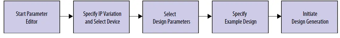 To generate the design example from the IP parameter editor:
- Create a project targeting Intel Agilex F-tile device family and select the desired device.
- In the IP Catalog, Tools ➤ IP Catalog, select F-Tile JESD204C Intel FPGA IP.
- Specify a top-level name and the folder for your custom IP variation. Click OK. The parameter editor adds the top-level .ip file to the current project automatically. If you are prompted to manually add the .ip file to the project, click Project ➤ Add/ Remove Files in Project to add the file.
- Under the Example Design tab, specify the design example parameters as described in Design Example Parameters.
- Click Generate Example Design.
The software generates all design files in the sub-directories. These files are required to run simulation and compilation.
Design Example Parameters
The F-Tile JESD204C Intel FPGA IP parameter editor includes the Example Design tab for you to specify certain parameters before generating the design example.
Table 6. Parameters in the Example Design Tab
| Parameter | Options | Description |
| Select Design |
| Select the system console control to access the design example data path through the system console. |
| Simulation | On, Off | Turn on for the IP to generate the necessary files for simulating the design example. |
| Synthesis | On, Off | Turn on for the IP to generate the necessary files for Intel Quartus Prime compilation and hardware demonstration. |
| HDL format (for simulation) |
| Select the HDL format of the RTL files for simulation. |
| HDL format (for synthesis) | Verilog only | Select the HDL format of the RTL files for synthesis. |
| Parameter | Options | Description |
| Generate 3- wire SPI module | On, Off | Turn on to enable 3-wire SPI interface instead of 4-wire. |
| Sysref mode |
| Select whether you want the SYSREF alignment to be a one-shot pulse mode, periodic, or gapped periodic, based on your design requirements and timing flexibility.
|
| Select board | None | Select the board for the design example.
|
| Test Pattern |
| Select pattern generator and checker test pattern.
|
| Enable internal serial loopback | On, Off | Select internal serial loopback. |
| Enable Command Channel | On, Off | Select command channel pattern. |
Directory Structure
The F-Tile JESD204C design example directories contain generated files for the design examples.
Figure 3. Directory Structure for F-Tile JESD204C Intel Agilex Design Example
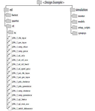 Table 7. Directory Files
| Folders | Files |
| ed/rtl |
|
| simulation/mentor |
|
| simulation/synopsys |
|
Simulating the Design Example Testbench
The design example testbench simulates your generated design.
Figure 4. Procedure
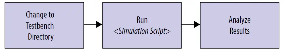 To simulate the design, perform the following steps:
- Change the working directory to <example_design_directory>/simulation/<Simulator>.
- In the command line, run the simulation script. The table below shows the commands to run the supported simulators.
| Simulator | Command |
| Questa/ModelSim | vsim -do modelsim_sim.tcl |
| vsim -c -do modelsim_sim.tcl (without Questa/ ModelSim GUI) | |
| VCS | sh vcs_sim.sh |
| VCS MX | sh vcsmx_sim.sh |
The simulation ends with messages that indicate whether the run was successful or not.
Figure 5. Successful Simulation
This figure shows the successful simulation message for VCS simulator.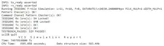
Compiling the Design Example
To compile the compilation-only example project, follow these steps:
- Ensure compilation design example generation is complete.
- In the Intel Quartus Prime Pro Edition software, open the Intel Quartus Prime Pro Edition project <example_ design_ directory>/ed/quartus.
- On the Processing menu, click Start Compilation.
Detailed Description for the F-Tile JESD204C Design Example
The F-Tile JESD204C design example demonstrates the functionality of data streaming using loopback mode.
You can specify the parameters settings of your choice and generate the design example.
The design example is available only in duplex mode for both Base and PHY variant. You can choose Base only or PHY only variant but the IP would generate the design example for both Base and PHY.
Note: Some high data rate configurations may fail timing. To avoid timing failure, consider specifying lower frame clock frequency multiplier (FCLK_MULP) value in the Configurations tab of the F-Tile JESD204C Intel FPGA IP parameter editor.
System Components
The F-Tile JESD204C design example provides a software-based control flow that uses the hard control unit with or without system console support.
The design example enables an auto link up in internal and external loopback modes.
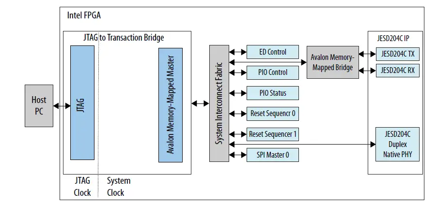
JTAG to Avalon Master Bridge
The JTAG to Avalon Master Bridge provides a connection between the host system to access the memory-mapped F-Tile JESD204C IP and the peripheral IP control and status registers through the JTAG interface.
Figure 6. System with a JTAG to Avalon Master Bridge Core
Note: System clock must be at least 2X faster than the JTAG clock. The system clock is mgmt_clk (100MHz) in this design example.
 Parallel I/O (PIO) Core
The parallel input/output (PIO) core with Avalon interface provides a memory-mapped interface between an Avalon memory-mapped slave port and general purpose I/O ports. The I/O ports connect either to on-chip user logic, or to I/O pins that connect to devices external to the FPGA.
Figure 7. PIO Core with Input Ports, Output Ports, and IRQ Support
By default, the Platform Designer component disables the Interrupt Service Line (IRQ).
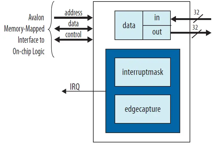 The PIO I/O ports are assigned at the top level HDL file ( io_ status for input ports, io_ control for output ports).
The table below describes the signal connectivity for the status and control I/O ports to the DIP switch and LED on the development kit.
Table 8. PIO Core I/O Ports
| Port | Bit | Signal |
| Out_port | 0 | USER_LED SPI programming done |
| 31:1 | Reserved | |
| In_port | 0 | USER_DIP internal serial loopback enable Off = 1 On = 0 |
| 1 | USER_DIP FPGA-generated SYSREF enable Off = 1 On = 0 | |
| 31:2 | Reserved. |
SPI Master
The SPI master module is a standard Platform Designer component in the IP Catalog standard library. This module uses the SPI protocol to facilitate the configuration of external converters (for example, ADC, DAC, and external clock generators) via a structured register space inside these devices.
The SPI master has an Avalon memory-mapped interface that connects to the Avalon master (JTAG to Avalon master bridge) via the Avalon memory-mapped interconnect. The SPI master receives configuration instructions from the Avalon master.
The SPI master module controls up to 32 independent SPI slaves. The SCLK baud rate is configured to 20 MHz (divisible by 5).
This module is configured to a 4-wire, 24-bit width interface. If the Generate 3-Wire SPI Module option is selected, an additional module is instantiated to convert the 4-wire output of the SPI master to 3-wire.
IOPLL
The IOPLL generates the clock required to generate frame_clk and link_clk. The reference clock to the PLL is configurable but limited to the data rate/factor of 33.
- For design example that supports data rate of 24.33024 Gbps, the clock rate for frame_clk and link_clk is 368.64 MHz.
- For design example that supports data rate of 32 Gbps, the clock rate for frame_clk and link_clk is 484.848 MHz.
SYSREF Generator
SYSREF is a critical timing signal for data converters with F-Tile JESD204C interface.
The SYSREF generator in the design example is used for the duplex JESD204C IP link initialization demonstration purpose only. In the JESD204C subclass 1 system level application,you must generate SYSREF from the same source as the device clock.
For the F-Tile JESD204C IP, the SYSREF multiplier (SYSREF_MULP) of the SYSREF control register defines the SYSREF period, which is n-integer multiple of the E parameter.
You must ensure E*SYSREF_MULP ≤16. For example, if E=1, the legal setting for SYSREF_MULP must be within 1–16, and if E=3, the legal setting for SYSREF_MULP must be within 1–5.
Note: If you set an out-of-range SYSREF_MULP, the SYSREF generator will fix the setting to SYSREF_MULP=1.
You can select whether you want the SYSREF type to be a one-shot pulse, periodic, or gapped periodic through the Example Design tab in the F-Tile JESD204C Intel FPGA IP parameter editor.
Table 9. Examples of Periodic and Gapped Periodic SYSREF Counter
| E | SYSREF_MULP | SYSREF PERIOD (E*SYSREF_MULP* 32) | Duty Cycle | Description |
| 1 | 1 | 32 | 1..31 (Programmable) | Gapped Periodic |
| 1 | 1 | 32 | 16 (Fixed) | Periodic |
| 1 | 2 | 64 | 1..63 (Programmable) | Gapped Periodic |
| 1 | 2 | 64 | 32 (Fixed) | Periodic |
| 1 | 16 | 512 | 1..511 (Programmable) | Gapped Periodic |
| 1 | 16 | 512 | 256 (Fixed) | Periodic |
| 2 | 3 | 19 | 1..191 (Programmable) | Gapped Periodic |
| 2 | 3 | 192 | 96 (Fixed) | Periodic |
| 2 | 8 | 512 | 1..511 (Programmable) | Gapped Periodic |
| 2 | 8 | 512 | 256 (Fixed) | Periodic |
| 2 | 9 (Illegal) | 64 | 32 (Fixed) | Gapped Periodic |
| 2 | 9 (Illegal) | 64 | 32 (Fixed) | Periodic |
Table 10. SYSREF Control Registers
You can dynamically reconfigure the SYSREF control registers if the register setting is different than the setting you specified when you generated the design example. Configure the SYSREF registers before the F-Tile JESD204C Intel FPGA IP is out of reset. If you select the external SYSREF generator through the
sysref_ctrl[7] register bit, you can ignore the settings for SYSREF type, multiplier, duty cycle and phase.
| Bits | Default Value | Description |
| sysref_ctrl[1:0] |
| SYSREF type. The default value depends on the SYSREF mode setting in the Example Design tab in the F-Tile JESD204C Intel FPGA IP parameter editor. |
| sysref_ctrl[6:2] | 5’b00001 | SYSREF multiplier. This SYSREF_MULP field is applicable to periodic and gapped-periodic SYSREF type. You must configure the multiplier value to ensure the E*SYSREF_MULP value is between 1 to 16 before the F-Tile JESD204C IP is out of reset. If the E*SYSREF_MULP value is out of this range, the multiplier value defaults to 5’b00001. |
| sysref_ctrl[7] |
| SYSREF select. The default value depends on the data path setting in the Example Design tab in the F-Tile JESD204C Intel FPGA IP parameter editor.
|
| sysref_ctrl[16:8] | 9’h0 | SYSREF duty cycle when SYSREF type is periodic or gapped periodic. You must configure the duty cycle before the F-Tile JESD204C IP is out of reset. Maximum value = (E*SYSREF_MULP*32)-1 For example: 50% duty cycle = (E*SYSREF_MULP*32)/2 The duty cycle defaults to 50% if you do not configure this register field, or if you configure the register field to 0 or more than the maximum value allowed. |
| sysref_ctrl[17] | 1’b0 | Manual control when SYSREF type is one-shot.
You need to write a 1 then a 0 to create a SYSREF pulse in one-shot mode. |
| sysref_ctrl[31:18] | 22’h0 | Reserved. |
Reset Sequencers
This design example consists of two reset sequencers:
- Reset Sequence 0—Handles the reset to TX/RX Avalon streaming domain, Avalon memory-mapped domain, core PLL, TX PHY, TX core, and SYSREF generator.
- Reset Sequence 1—Handles the reset to RX PHY and RX Core.
3-Wire SPI
This module is optional to convert SPI interface to 3-wire.
System PLL
F-tile has three on-board system PLLs. These system PLLs are the primary clock source for hard IP (MAC, PCS, and FEC) and EMIB crossing. This means that, when you use the system PLL clocking mode, the blocks are not clocked by the PMA clock and do not depend on a clock coming from the FPGA core. Each system PLL only generates the clock associated with one frequency interface. For example, you need two system PLLs to run one interface at 1 GHz and one interface at 500 MHz. Using a system PLL allows you to use every lane independently without a lane clock change affecting a neighboring lane.
Each system PLL can use any one of eight FGT reference clocks. System PLLs can share a reference clock or have different reference clocks. Each interface can choose which system PLL it uses, but, once chosen, it is fixed, not reconfigurable using dynamic reconfiguration.
Related Information
F-tile Architecture and PMA and FEC Direct PHY IP User Guide
More information about the system PLL clocking mode in Intel Agilex F-tile devices.
Pattern Generator and Checker
The pattern generator and checker are useful for creating data samples and monitoring for testing purposes.
Table 11. Supported Pattern Generator
| Pattern Generator | Description |
| PRBS pattern generator | The F-Tile JESD204C design example PRBS pattern generator supports the following degree of polynomials:
|
| Ramp pattern generator | The ramp pattern value increments by 1 for every subsequent sample with the generator width of N, and rolls over to 0 when all bits in the sample are 1. Enable the ramp pattern generator by writing a 1 to bit 2 of the tst_ctl register of the ED control block. |
| Command channel ramp pattern generator | The F-Tile JESD204C design example supports command channel ramp pattern generator per lane. The ramp pattern value increments by 1 per 6 bits of command words. The starting seed is an increment pattern across all lanes. |
Table 12. Supported Pattern Checker
| Pattern Checker | Description |
| PRBS pattern checker | The scrambling seed in the pattern checker is self- synchronized when the F-Tile JESD204C IP achieves deskew alignment. The pattern checker requires 8 octets for the scrambling seed to self-synchronize. |
| Ramp pattern checker | The first valid data sample for each converter (M) is loaded as the initial value of the ramp pattern. Subsequent data samples values must increase by 1 in each clock cycle up to the maximum and then roll over to 0. |
| Pattern Checker | Description |
| For example, when S=1, N=16 and WIDTH_MULP = 2, the data width per converter is S * WIDTH_MULP * N = 32. The maximum data sample value is 0xFFFF. The ramp pattern checker verifies that identical patterns are received across all converters. | |
| Command channel ramp pattern checker | The F-Tile JESD204C design example supports command channel ramp pattern checker. The first command word (6 bits) received is loaded as the initial value. Subsequent command words in the same lane must increment up to 0x3F and roll over to 0x00. The command channel ramp pattern checker checks for ramp patterns across all lanes. |
F-Tile JESD204C TX and RX IP
This design example allows you to configure each TX/RX in simplex mode or duplex mode.
Duplex configurations allow IP functionality demonstration using either internal or external serial loopback. CSRs within the IP are not optimized away to allow for IP control and status observation.
F-Tile JESD204C Design Example Clock and Reset
The F-Tile JESD204C design example has a set of clock and reset signals.
Table 13.Design Example Clocks
| Clock Signal | Direction | Description |
| mgmt_clk | Input | LVDS differential clock with frequency of 100 MHz. |
| refclk_xcvr | Input | Transceiver reference clock with frequency of data rate/factor of 33. |
| refclk_core | Input | Core reference clock with the same frequency as refclk_xcvr. |
| in_sysref | Input | SYSREF signal. Maximum SYSREF frequency is data rate/(66x32xE). |
| sysref_out | Output | |
| txlink_clk rxlink_clk | Internal | TX and RX link clock with frequency of data rate/66. |
| txframe_clk rxframe_clk | Internal |
|
| tx_fclk rx_fclk | Internal |
|
| spi_SCLK | Output | SPI baud rate clock with frequency of 20 MHz. |
When you load the design example into an FPGA device, an internal ninit_done event ensures that the JTAG to Avalon Master bridge is in reset as well as all the other blocks.
The SYSREF generator has its independent reset to inject intentional asynchronous relationship for the txlink_clk and rxlink_clk clocks. This method is more comprehensive in emulating the SYSREF signal from an external clock chip.
Table 14. Design Example Resets
| Reset Signal | Direction | Description |
| global_rst_n | Input | Push button global reset for all blocks, except the JTAG to Avalon Master bridge. |
| ninit_done | Internal | Output from Reset Release IP for the JTAG to Avalon Master bridge. |
| edctl_rst_n | Internal | The ED Control block is reset by JTAG to Avalon Master bridge. The hw_rst and global_rst_n ports do not reset the ED Control block. |
| hw_rst | Internal | Assert and deassert hw_rst by writing to the rst_ctl register of the ED Control block. mgmt_rst_in_n asserts when hw_rst is asserted. |
| mgmt_rst_in_n | Internal | Reset for Avalon memory-mapped interfaces of various IPs and inputs of reset sequencers:
|
| sysref_rst_n | Internal | Reset for SYSREF generator block in the ED Control block using the reset sequencer 0 reset_out2 port. The reset sequencer 0 reset_out2 port deasserts the reset if the core PLL is locked. |
| core_pll_rst | Internal | Resets the core PLL through the reset sequencer 0 reset_out0 port. The core PLL resets when mgmt_rst_in_n reset is asserted. |
| j204c_tx_avs_rst_n | Internal | Resets the F-Tile JESD204C TX Avalon memory- mapped interface through reset sequencer 0. The TX Avalon memory-mapped interface asserts when mgmt_rst_in_n is asserted. |
| j204c_rx_avs_rst_n | Internal | Resets the F-Tile JESD204C TX Avalon memory- mapped interface through reset sequencer 1. The RX Avalon memory-mapped interface asserts when mgmt_rst_in_n is asserted. |
| j204c_tx_rst_n | Internal | Resets the F-Tile JESD204C TX link and transport layers in txlink_clk, and txframe_clk, domains. The reset sequencer 0 reset_out5 port resets j204c_tx_rst_n. This reset deasserts if the core PLL is locked, and the tx_pma_ready and tx_ready signals are asserted. |
| j204c_rx_rst_n | Internal | Resets the F-Tile JESD204C RX link and transport layers in, rxlink_clk,and rxframe_clk domains. |
| Reset Signal | Direction | Description |
| The reset sequencer 1 reset_out4 port resets j204c_rx_rst_n. This reset deasserts if the core PLL is locked, and the rx_pma_ready and rx_ready signals are asserted. | ||
| j204c_tx_rst_ack_n | Internal | Reset handshakes signal with j204c_tx_rst_n. |
| j204c_rx_rst_ack_n | Internal | Reset handshakes signal with j204c_rx_rst_n. |
Figure 8. Timing Diagram for the Design Example Resets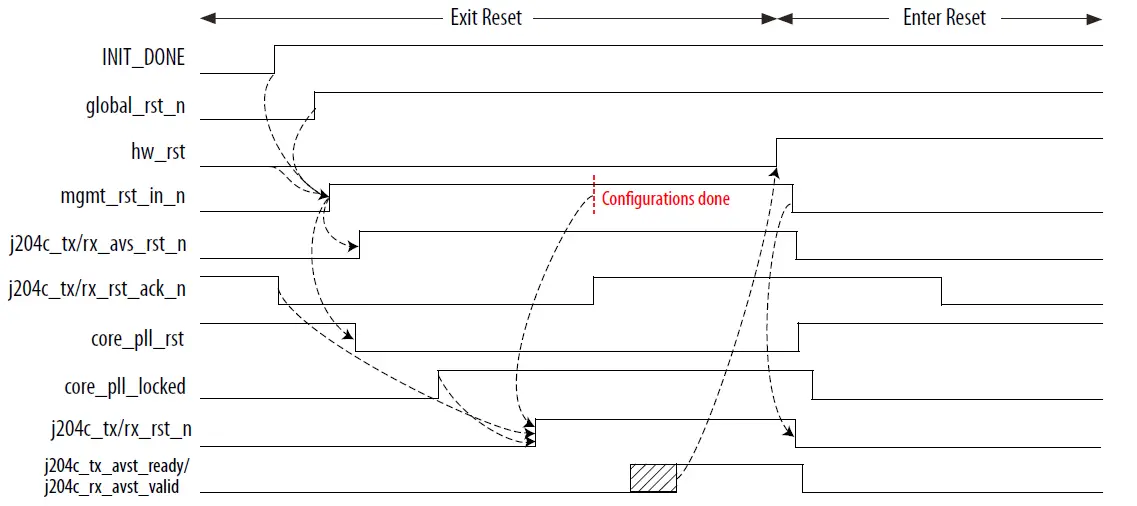
F-Tile JESD204C Design Example Signals
Table 15. System Interface Signals
| Signal | Direction | Description |
| Clocks and Resets | ||
| mgmt_clk | Input | 100 MHz clock for system management. |
| refclk_xcvr | Input | Reference clock for F-tile UX QUAD and System PLL. Equivalent to data rate/factor of 33. |
| refclk_core | Input | Core PLL reference clock. Applies the same clock frequency as refclk_xcvr. |
| in_sysref | Input | SYSREF signal from external SYSREF generator for JESD204C Subclass 1 implementation. |
| sysref_out | Output | SYSREF signal for JESD204C Subclass 1 implementation generated by the FPGA device for design example link initialization purpose only. |
| Signal | Direction | Description |
| SPI | ||
| spi_SS_n[2:0] | Output | Active low, SPI slave select signal. |
| spi_SCLK | Output | SPI serial clock. |
| spi_sdio | Input/Output | Output data from the master to external slave. Input data from external slave to master. |
| Signal | Direction | Description |
| Note:When Generate 3-Wire SPI Module option is enabled. | ||
| spi_MISO Note: When Generate 3-Wire SPI Module option is not enabled. | Input | Input data from external slave to the SPI master. |
| spi_MOSI Note: When Generate 3-Wire SPI Module option is not enabled. | Output | Output data from SPI master to the external slave. |
| Signal | Direction | Description |
| ADC/DAC | ||
| tx_serial_data[LINK*L-1:0] | Output | Differential high speed serial output data to DAC. The clock is embedded in the serial data stream. |
| tx_serial_data_n[LINK*L-1:0] | ||
| rx_serial_data[LINK*L-1:0] | Input | Differential high speed serial input data from ADC. The clock is recovered from the serial data stream. |
| rx_serial_data_n[LINK*L-1:0] | ||
| Signal | Direction | Description |
| General Purpose I/O | ||
| user_led[3:0] |
Output | Indicates the status for the following conditions:
|
| user_dip[3:0] | Input | User mode DIP switch input:
|
| Signal | Direction | Description |
| Out-of-band (OOB) and Status | ||
| rx_patchk_data_error[LINK-1:0] | Output | When this signal is asserted, it indicates pattern checker has detected error. |
| rx_link_error[LINK-1:0] | Output | When this signal is asserted, it indicates JESD204C RX IP has asserted interrupt. |
| tx_link_error[LINK-1:0] | Output | When this signal is asserted, it indicates JESD204C TX IP has asserted interrupt. |
| emb_lock_out | Output | When this signal is asserted, it indicates JESD204C RX IP has achieved EMB lock. |
| sh_lock_out | Output | When this signal is asserted, it indicates JESD204C RX IP sync header is locked. |
| Signal | Direction | Description |
| Avalon Streaming | ||
| rx_avst_valid[LINK-1:0] | Input | Indicates whether the converter sample data to the application layer is valid or invalid.
|
| rx_avst_data[(TOTAL_SAMPLE*N)-1:0 ] | Input | Converter sample data to the application layer. |
F-Tile JESD204C Design Example Control Registers
The F-Tile JESD204C design example registers in the ED Control block use byte-addressing (32 bits).
Table 16. Design Example Address Map
These 32-bit ED Control block registers are in the mgmt_clk domain.
| Component | Address |
| F-Tile JESD204C TX IP | 0x000C_0000 – 0x000C_03FF |
| F-Tile JESD204C RX IP | 0x000D_0000 – 0x000D_03FF |
| SPI Control | 0x0102_0000 – 0x0102_001F |
| PIO Control | 0x0102_0020 – 0x0102_002F |
| PIO Status | 0x0102_0040 – 0x0102_004F |
| Reset Sequencer 0 | 0x0102_0100 – 0x0102_01FF |
| Reset Sequencer 1 | 0x0102_0200 – 0x0102_02FF |
| ED Control | 0x0102_0400 – 0x0102_04FF |
| F-Tile JESD204C IP transceiver PHY Reconfig | 0x0200_0000 – 0x023F_FFFF |
Table 17. Register Access Type and Definition
This table describes the register access type for Intel FPGA IPs.
| Access Type | Definition |
| RO/V | Software read-only (no effect on write). The value may vary. |
| RW |
|
| RW1C |
|
Table 18. ED Control Address Map
| Offset | Register Name |
| 0x00 | rst_ctl |
| 0x04 | rst_sts0 |
| continued… | |
| Offset | Register Name |
| 0x10 | rst_sts_detected0 |
| 0x40 | sysref_ctl |
| 0x44 | sysref_sts |
| 0x80 | tst_ctl |
| 0x8c | tst_err0 |
Table 19. ED Control Block Control and Status Registers
| Byte Offset | Register | Name | Access | Reset | Description |
| 0x00 | rst_ctl | rst_assert | RW | 0x0 | Reset control. [0]: Write 1 to assert reset. (hw_rst) Write 0 again to deassert reset. [31:1]: Reserved. |
| 0x04 | rst_sts0 | rst_status | RO/V | 0x0 | Reset status. [0]: Core PLL locked status. [31:1]: Reserved. |
| 0x10 | rst_sts_dete cted0 | rst_sts_set | RW1C | 0x0 | SYSREF edge detection status for internal or external SYSREF generator. [0]: Value of 1 Indicates a SYSREF rising edge is detected for subclass 1 operation. Software may write 1 to clear this bit to enable new SYSREF edge detection. [31:1]: Reserved. |
| 0x40 | sysref_ctl | sysref_contr ol | RW | Duplex datapath
| SYSREF control. Refer to Table 10 on page 17 for more information about the usage of this register. |
| Periodic: | Note: The reset value depends on | ||||
| 0x00081 | the SYSREF type and F-Tile | ||||
| Gapped- periodic: | JESD204C IP data path parameter settings. | ||||
| 0x00082 | |||||
| TX or RX data | |||||
| path | |||||
| One-shot: | |||||
| 0x00000 | |||||
| Periodic: | |||||
| 0x00001 | |||||
| Gapped- | |||||
| periodic: | |||||
| 0x00002 | |||||
| 0x44 | sysref_sts | sysref_statu s | RO/V | 0x0 | SYSREF status. This register contains the latest SYSREF period and duty cycle settings of the internal SYSREF generator. Refer to Table 9 on page 16 for the legal value of the SYSREF period and duty cycle. |
| continued… | |||||
| Byte Offset | Register | Name | Access | Reset | Description |
[8:0]: SYSREF period.
| |||||
| 0x80 | tst_ctl | tst_control | RW | 0x0 | Test control. Use this register to enable different test patterns for the pattern generator and checker. [1:0] = Reserved field [2] = ramp_test_ctl
[31:3]: Reserved. |
| 0x8c | tst_err0 | tst_error | RW1C | 0x0 | Error flag for Link 0. When the bit is 1’b1, it indicates an error has happened. You should resolve the error before writing 1’b1 to the respective bit to clear the error flag. [0] = Pattern checker error [1] = tx_link_error [2] = rx_link_error [3] = Command pattern checker error [31:4]: Reserved. |
Document Revision History for the F-Tile JESD204C Intel FPGA IP Design Example User Guide
| Document Version | Intel Quartus Prime Version | IP Version | Changes |
| 2021.10.11 | 21.3 | 1.0.0 | Initial release. |


 Agilex Fpga Ip Design Example User Guide")


