HOLTEK Bestcomm RFs BCE-GENTrxN-00z Development Board User Guide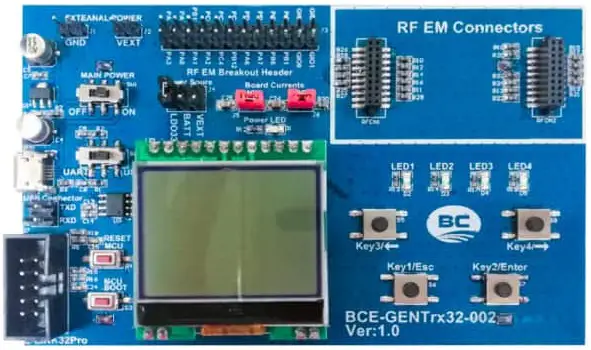
Abstract
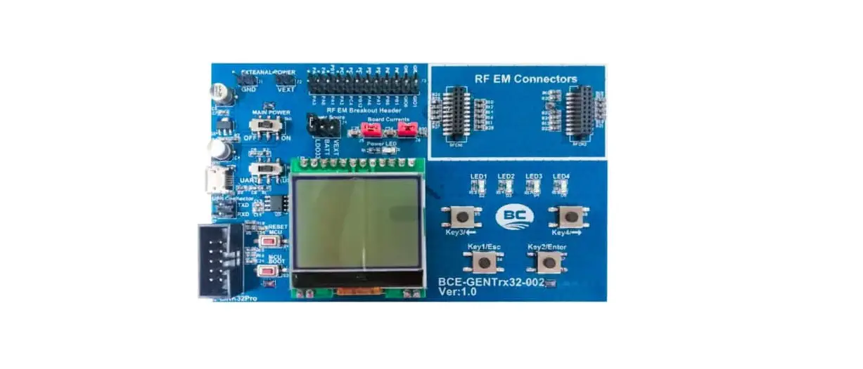
Bestcomm RF’s BCE-GENTrxN-00z development board is divided into three types (without MCU and with HT8, HT32) for users to evaluate and develop wireless products.
| PN | Description |
| BCE-GENTrx0-00z | Without MCU |
| BCE-GENTRX8-00z | With HT8 MCU (8-bit) |
| BCE-GENTRX32-00z | With HT32 MCU (32-bit) |
Note:
Z : Version
N: Type
System diagram
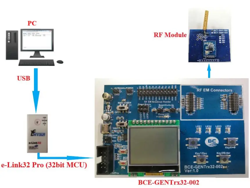
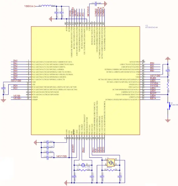
The following figure shows the system architecture of the development board. The main control chip of the development board is HT32F52352。Users can use e-Link32 Pro (32-bit MCU) development tools for programming and development according to different types of RF modules.
Hardware diagram
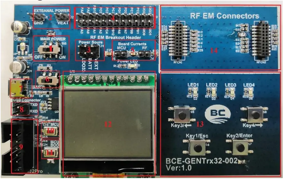
- Power switch(ON/OFF):
This is the system power switch。 - External power input port:
User can directly supply power to the whole system through this pin. If an external power supply is required, the power source selection pin (vext) needs to be set. - System power selection (Jump)
The system power source selection (Jump) can choose VEXT (external power port), LDO33 (LDO output), BATT (AAx2 series battery) four kinds - I/O interface
Connect the pin what want to use - CU and RF module power supply port(Jump):
When the MCU needs power supply, this port needs to be shorted and this port can also be used as the measurement point of the operating current loop. When the RF module needs power supply, this port needs to be shorted and this port can also be used as the measurement point of the operating current loop. - Serial port selector switch
User can through this switch select the micro USB interface to connect directly to the USB data bus of HT32 (select USB) or connect to the USB to serial bridge IC, then to HT32 (select UART). - USB interface
The Micro-USB interface can be used as the input source of the LDO and can also be used to directly supply power to the development board and also supports COM communication. - UART interface
This pin is the UART out port on the development board. This interface is used to lead out the USB data bus of ht32 (the serial port selection switch selects USB) and the TXD/RXD pins of JTAG - Emulation/programming interface:
This interface can be used with e-Link32 Pro emulation and programming and can also be connected to E-Writer32 programming. - System reset button
This button is used for MCU reset. - MCU start mode Key
Press this key when 32-bit MCU needs to be started by boot loader 32Bit Mcu need - LCM Module:
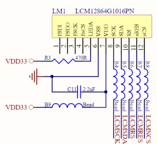
This LCM model is SN74LVC8T245 (128×64 display)。 - LEDs x 4 Buttons x4
Used as GPIO output(indication) and input function. - Module interface
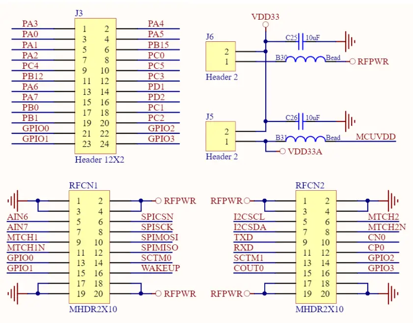
Supports BM2302-0X-1、BM3602-0X-1、BM5602-60-1 RF modules.
Schematic diagram
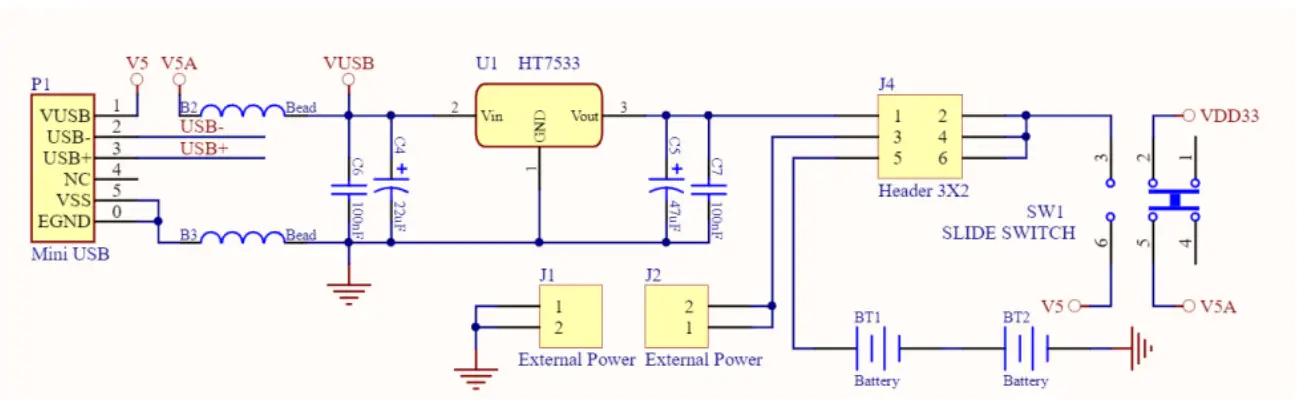
- Power circuit:

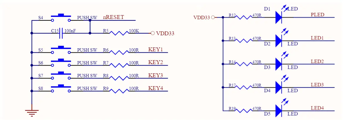
- LED & Button circuit:

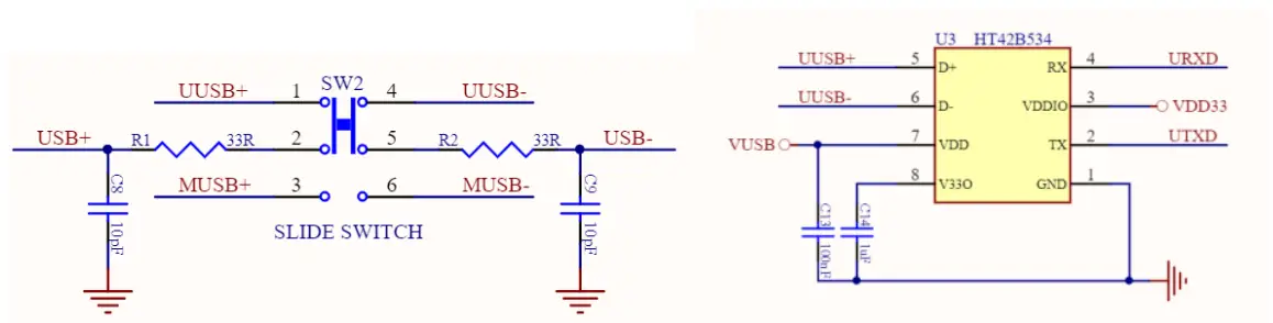
- Serial switch and USB to TTL Interface circuit:

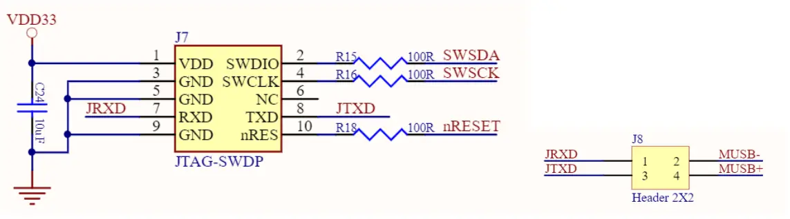
- JTAG(E-LINK32Pro) Interface & USB 2.0 Interface

- LCM interface circuit

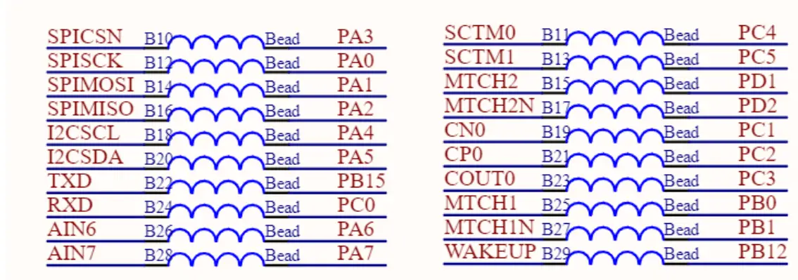
- I/O and RF Module interface circuit


- MCU system circuit