intel AN 496 Using the Internal Oscillator IP Core
Using the Internal Oscillator IP Core
The supported Intel® devices offer a unique internal oscillator feature. As shown in the design examples described in this application note, internal oscillators make an excellent choice to implement designs that require clocking, thereby saving on-board space and costs associated with external clocking circuitry.
Related Information
- Design Example for MAX® II
- Provides the MAX® II design files for this application note (AN 496).
- Design Example for MAX® V
- Provides the MAX® V design files for this application note (AN 496).
- Design Example for Intel MAX® 10
- Provides the Intel MAX® 10 design files for this application note (AN 496).
Internal Oscillators
Most designs require a clock for normal operation. You can use the internal oscillator IP core for clock source in user design or debug purposes. With an internal oscillator, the supported Intel devices do not require external clocking circuitry. For example, you can use the internal oscillator to meet the clocking requirement of an LCD controller, system management bus (SMBus) controller, or any other interfacing protocol, or to implement a pulse width modulator. This helps minimize component count, board space, and reduces the total cost of the system. You can instantiate the internal oscillator without instantiating the user flash memory (UFM) by using the supported Intel devices’ oscillator IP core in the Intel Quartus® Prime software for MAX® II and MAX V devices. For Intel MAX 10 devices, the oscillators are separate from the UFM. The oscillator’s output frequency, osc, is one-fourth of the undivided frequency of the internal oscillator.
Frequency Range for Supported Intel Devices
| Devices | Output Clock from Internal Oscillator (1) (MHz) |
| MAX II | 3.3 – 5.5 |
| MAX V | 3.9 – 5.3 |
| Intel MAX 10 | 55 – 116 (2), 35 – 77 (3) |
- The output port for internal oscillator IP core is osc in MAX II and MAX V devices, and clkout in all other supported devices.
| Devices | Output Clock from Internal Oscillator (1) (MHz) |
| Cyclone® III (4) | 80 (max) |
| Cyclone IV | 80 (max) |
| Cyclone V | 100 (max) |
| Intel Cyclone 10 GX | 100 (max) |
| Intel Cyclone 10 LP | 80 (max) |
| Arria® II GX | 100 (max) |
| Arria V | 100 (max) |
| Intel Arria 10 | 100 (max) |
| Stratix® V | 100 (max) |
| Intel Stratix 10 | 170 – 230 |
- The output port for internal oscillator IP core is osc in MAX II and MAX V devices, and clkout in all other supported devices.
- For 10M02, 10M04, 10M08, 10M16, and 10M25.
- For 10M40 and 10M50.
- Supported in the Intel Quartus Prime software version 13.1 and earlier.
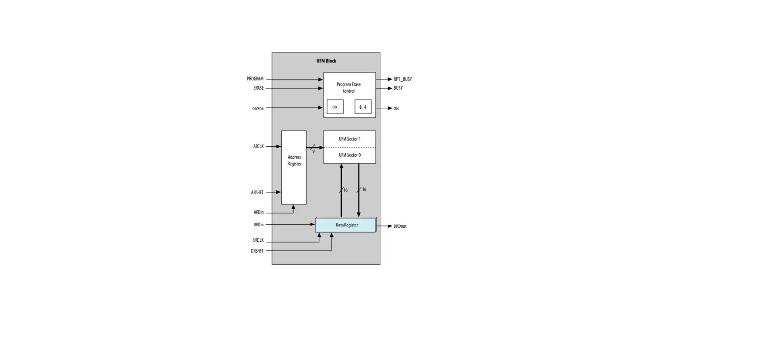
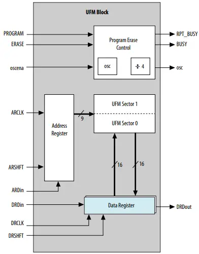
Internal Oscillator as Part of the UFM for MAX II and MAX V Devices
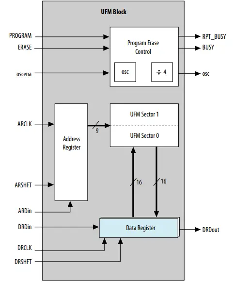
The internal oscillator is part of the Program Erase Control block, which controls the programming and erasing of the UFM. The data register holds the data to be sent or retrieved from the UFM. The address register holds the address from which data is retrieved or the address to which the data is written. The internal oscillator for the UFM block is enabled when the ERASE, PROGRAM, and READ operation is executed.
Pin Description for the Internal Oscillator IP Core
| Signal | Description |
| oscena | Use to enable the internal oscillator. Input high to enable the oscillator. |
| osc/clkout (5) | Output of the internal oscillator. |
Using the Internal Oscillator in MAX II and MAX V Devices
The internal oscillator has a single input, oscena, and a single output, osc. To activate the internal oscillator, use oscena. When activated, a clock with the frequency is made available at the output. If oscena is driven low, the output of the internal oscillator is a constant high.
To instantiate the internal oscillator, follow these steps
- On the Tools menu of the Intel Quartus Prime software, click IP Catalog.
- Under the Library category, expand the Basic Functions and I/O.
- Select MAX II/MAX V oscillator and after clicking Add, the IP Parameter Editor appears. You can now select the oscillator output frequency.
- In Simulation Libraries, the model files that must be included are listed. Click Next.
- Select the files to be created. Click Finish. The selected files are created and can be accessed from the output file folder. After the instantiation code is added to the file, the oscena input must be made as a wire and assigned as a logic value of “1” to enable the oscillator.
Using the Internal Oscillator in All Supported Devices (except MAX II and MAX V devices)
The internal oscillator has a single input, oscena, and a single output, osc. To activate the internal oscillator, use oscena. When activated, a clock with the frequency is made available at the output. If oscena is driven low, the output of the internal oscillator is a constant low.
To instantiate the internal oscillator, follow these steps
- On the Tools menu of the Intel Quartus Prime software, click IP Catalog.
- Under the Library category, expand the Basic Functions and Configuration Programming.
- Select Internal Oscillator (or Intel FPGA S10 Configuration Clock for Intel Stratix 10 devices) and after clicking Add, the IP Parameter Editor appears.
- In the New IP Instance dialog box:
- Set the top-level name of your IP.
- Select the Device family.
- Select the Device.
- Click OK.
- To generate the HDL, click Generate HDL.
- Click Generate.
The selected files are created and can be accessed from the output file folder as specified in the output directory path. After the instantiation code is added to the file, the oscena input must be made as a wire and assigned as a logic value of “1” to enable the oscillator.
Implementation
You can implement these design examples with MAX II, MAX V, and Intel MAX 10 devices, all of which have the internal oscillator feature. Implementation involves demonstration of the internal oscillator function by assigning the oscillator output to a counter and driving the general purpose I/O (GPIO) pins on MAX II, MAX V, and Intel MAX 10 devices.
Design Example 1: Targeting a MDN-82 Demo Board (MAX II Devices)
Design Example 1 is made to drive the LEDs to create a scrolling effect, thereby demonstrating the internal oscillator using the MDN-82 demo board.
EPM240G Pin Assignments for Design Example 1 Using the MDN-82 Demo Board
| EPM240G Pin Assignments | |||
| Signal | Pin | Signal | Pin |
| d2 | Pin 69 | d3 | Pin 40 |
| d5 | Pin 71 | d6 | Pin 75 |
| d8 | Pin 73 | d10 | Pin 73 |
| d11 | Pin 75 | d12 | Pin 71 |
| d4_1 | Pin 85 | d4_2 | Pin 69 |
| d7_1 | Pin 87 | d7_2 | Pin 88 |
| d9_1 | Pin 89 | d9_2 | Pin 90 |
| sw9 | Pin 82 | — | — |
Assign the unused pins As input tri-stated in the Intel Quartus Prime software.
To demonstrate this design on the MDN-B2 demo board, follow these steps
- Turn on the power to the demo board (using slide switch SW1).
- Download the design onto the MAX II CPLD through the JTAG header JP5 on the demo board and a conventional programming cable (Intel FPGA Parallel Port Cable or Intel FPGA Download Cable). Keep SW4 on the demo board pressed before and during the start of the programming process. After it completes, turn off the power and remove the JTAG connector.
- Observe the scrolling LED sequence on the red LEDs and the bi-color LEDs. Pressing SW9 on the demo board disables the internal oscillator and the scrolling LEDs will freeze at their current positions.
Design Example 2: Targeting a MAX V Device Development Kit
In Design Example 2, the oscillator output frequency is divided by 221 before clocking a 2-bit counter. The output of this 2-bit counter is used to drive the LEDs, thereby demonstrating the internal oscillator on the MAX V device development kit.
5M570Z Pin Assignments for Design Example 2 Using the MAX V Device Development Kit
| 5M570Z Pin Assignments | |||
| Signal | Pin | Signal | Pin |
| pb0 | M9 | LED[0] | P4 |
| osc | M4 | LED[1] | R1 |
| clk | P2 | — | — |
To demonstrate this design on the MAX V development kit, follow these steps
- Plug in the USB cable into the USB Connector to power up the device.
- Download the design onto the MAX V device through the embedded Intel FPGA Download Cable.
- Observe the blinking LEDs (LED[0] and LED[1]). Pressing pb0 on the demo board disables the internal oscillator and the blinking LEDs will freeze at their current state.
Document Revision History for AN 496: Using the Internal Oscillator IP Core
| Date | Version | Changes |
| November 2017 | 2017.11.06 |
|
| November 2014 | 2014.11.04 | Updated the frequency for undivided internal oscillator and output clock from internal oscillator frequency values for MAX 10 devices in the Frequency Range for Supported Altera Devices table. |
| September 2014 | 2014.09.22 | Added MAX 10 devices. |
| January 2011 | 2.0 | Updated to include MAX V devices. |
| December 2007 | 1.0 | Initial release. |
ID: 683653
Version: 2017.11.06


