tuya VWRK4 AVS Smart Audio Installation Guide
Product Abstract
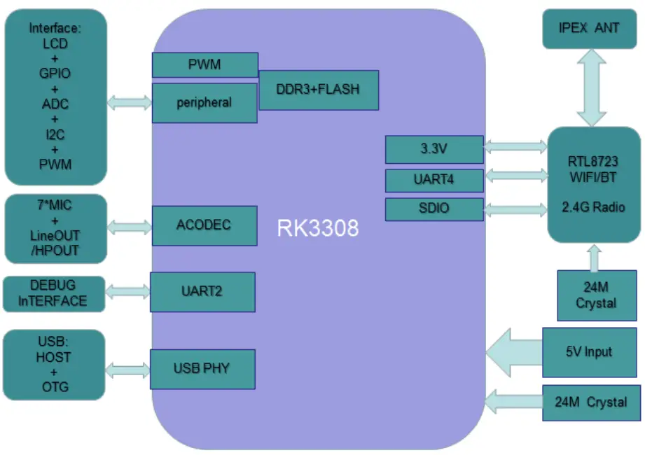
Tuya AVS voice module VWRK4 is based on the powerful RockChip 3308 IC which integrated with 4-Core 64 bit A35 ARM Core. The Module is integrated with voice wake & noise cancellation algorithm and which can be applied in the IoT device/gateway/smart speaker. The CPU RK3308’s frequency is 1.3GHz, which can provide powerful computing ability. Also, the module is integrated with the RF chip RTL8723DS which contains WiFi Sing-band 1X1+BluetoothBR/EDR/BLE4.0 This can make it easy to connect to the Tuya IoT platform.
Features
- High powerful ARM 4-Core 64 bit A35 RochChip 3308 CPU
- Frequency: 1.3GHz
- Work voltage: 4.2-5.5V(5V default)
- Peripheral: 2*Uart,7*MIC,RGB666,1*SPI,2*I2C 2*USB, GPIOs,3*ADC,
- Antenna: IPEX
- Sampling Rate: 16K/16bit
- Audio Feature
- 4 ways mic pickup, stereo playback.
- 6 ways mic pickup, single channel playback.
- Audio output: stereo HPOUT and stereo LINEOUT
- Audio AUX IN: support
- Entertainment:
Approved: amazon music, audible, iHeartRadio, TuneIn - Skill: All the skills contains in Alexa. For example:
Newest arrivals, Business & finance, Connected Car,Education & Reference, Food &Drink, Game & Trivia, Health & Fitness, kids, lifestyle, local, Movies & TV, Music & Audio, News, Novelty & Humor, Productivity, Shopping, Smart Home, Sports, Travel & Transportation, Utilities,Weather.
Applications
- Smart household and home appliances
- Smart Device
- Net Gateway Control
- Voice Control Panel
Module Interfaces
Dimensions and Footprint
The Module has four rows of pins with 1mm Pin Width and 1.5mm pin spacing,the total number of pins is 82,and its dimensions is 35mm*35mm*3.2mm (W*L*H),Figure 2-1 shows the Dimension views.
Note:
The default dimensional tolerance is ±0.35mm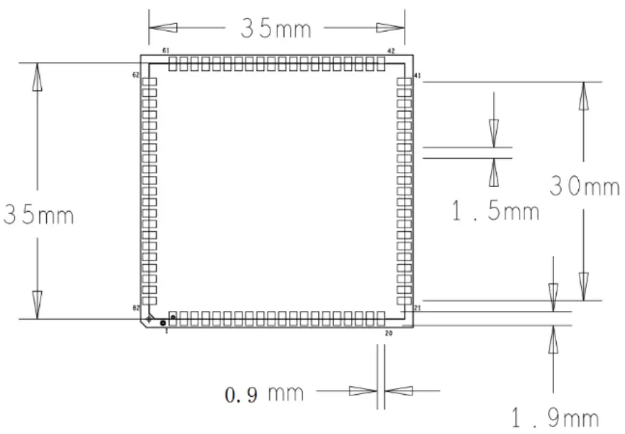
Figure 2-1 Dimensions of VWRK4
The total pins is 82 and the opposite side has the same number pins, one side is 20 and the other is 21. Figure 2-2 shows the footprint views.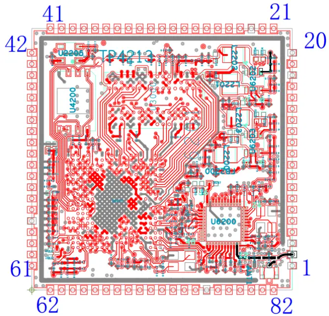
Figure 2-2 Footprint of VWRK4
Circuit Diagram
Table 2-1 Hardware Feature
| MCU | RK3308 | 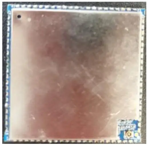 |
| Flash | 128 MByte | |
| DDR | 128 MByte | |
| Mic | 2/4 mic array | |
| BT | BluetoothBR/EDR/BLE4.0 | |
| WIFI | IEEE 802.11b/g/n (channel 1-14) | |
| Power Interface | MicroUSB 5V1A | |
| Antenna | IPEX Antenna | |
| Audio | MIC/HPOUT/LINEOUT | |
| LCD | LCD Interface | |
| Interface | Reserved UART/IIC/PWM/GPIO/USB interface | |
- Circuit Diagram of VWRK4 voice kit

Figure 2-3 Circuit Diagram of VWRK4
Pin Definition
Table 2-2 Pin Definition of VWRK4
Pin No. | Pin Name | Pad Type | Function |
| 1 | GND | P | Power Supply reference ground pin |
| 2 | ANT | O | The RF ANT Interface |
| 3 | GND | P | Power Supply reference ground pin |
| 4 | ADC_KEY_IN2 | AI | Analog of ADC Input |
| 5 | SAR_ADC_IN3 | AI | Analog of ADC Input |
| 6 | UNO_RX | I/O | Debug UART RX |
| 7 | UNO_TX | I/O | Debug UART TX |
| 8 | USB_HOST_DM | I/O | USB Data PIN for Host |
| 9 | USB_HOST_DP | I/O | USB Data PIN for Host |
| 10 | USB_OTG_ID | I/O | USB ID PIN for OTG |
| 11 | USB_OTG_DM | I/O | USB Data PIN for OTG |
| 12 | USB_OTG_DP | I/O | USB Data PIN for OTG |
| 13 | PHONE_CTRL | I/O | The General I/O Pin |
| 14 | PHONE_DET | I/O | The General I/O Pin |
| 15 | AUX_IN_CTRL | I/O | Selection of HPout or Lineout/ General I/O |
| 16 | SPK_MUTE | I/O | Speaker mute Control Pin /The General I/O Pin |
| 17 | MIC_LED | I/O | Control of Led Peripherals/ General I/O |
| 18 | GND | P | Power Supply reference ground pin |
| 19 | VCC-IO_OUT | P | Power supply pin for Peripherals |
| 20 | GND | P | Power Supply reference ground pin |
| 21 | VCC-5V | P | Power supply pin(5V) |
| 22 | VCC-5V | P | Power supply pin(5V) |
| 23 | GND | P | Power Supply reference ground pin |
| 24 | IR_RX | I/O | IR Receive Pin / General IO Pin |
| 25 | IR_TX | I/O | IR Tranmit Pin / General IO Pin |
| 26 | I2C_SDA | I/O | I2C SDA for Peripherals |
| 27 | I2C_CLK | I/O | I2C CLK for Peripherals |
| 28 | LCD_PWR | I/O | LCD Power Control Pin |
| 29 | LCD_BL | I/O | LCD Back light / General IO Pin/PWM |
| 30 | LCD_RST | I/O | LCD Reset Pin / General IO Pin |
| 31 | LCD_DEN | I/O | LCD Data Enable/ General IO Pin |
| 32 | LCD_HS | I/O | LCD Horizontal sync PIN/ General IO Pin |
| 33 | LCD_VS | I/O | LCD Vertical sync PIN/ General IO Pin |
| 34 | LCD_CLK | I/O | LCD Clk Pin / General IO Pin |
| 35 | LCD_D0 | I/O | LCD Data Pin / General IO Pin |
| 36 | LCD_D1 | I/O | LCD Data Pin / General IO Pin |
| 37 | LCD_D2 | I/O | LCD Data Pin / General IO Pin |
| 38 | LCD_D3 | I/O | LCD Data Pin / General IO Pin |
| 39 | LCD_D4 | I/O | LCD Data Pin / General IO Pin |
| 40 | LCD_D5 | I/O | LCD Data Pin / General IO Pin |
| 41 | LCD_D6 | I/O | LCD Data Pin / General IO Pin |
| 42 | LCD_D11 | I/O | LCD Data Pin / General IO Pin |
| 43 | LCD_D10 | I/O | LCD Data Pin / General IO Pin |
| 44 | LCD_D8 | I/O | LCD Data Pin / General IO Pin |
| 45 | LCD_D7 | I/O | LCD Data Pin / General IO Pin |
| 46 | LCD_D13 | I/O | LCD Data Pin / General IO Pin |
| 47 | LCD_D14 | I/O | LCD Data Pin / General IO Pin |
| 48 | LCD_D9 | I/O | LCD Data Pin / General IO Pin |
| 49 | LCD_D17 | I/O | LCD Data Pin / General IO Pin |
| 50 | LCD_D12 | I/O | LCD Data Pin / General IO Pin |
| 51 | LCD_D15 | I/O | LCD Data Pin / General IO Pin |
| 52 | LCD_D16 | I/O | LCD Data Pin / General IO Pin |
| 53 | LCD_SPI_RX | I/O | SPI Data Pin for LCD / General IO Pin |
| 54 | LCD_SPI_CLK | I/O | SPI CLk Pin for LCD / General IO Pin |
| 55 | LCD_SPI_CS | I/O | SPI CS Pin for LCD / General IO Pin |
| 56 | LCD_SPI_TX | I/O | SPI Data Pin for LCD / General IO Pin |
| 57 | GND | P | Power Supply reference ground pin |
| 58 | HPOUT_R | AO | Headphone output Right |
| 59 | HPOUT_L | AO | Headphone output Left |
| 60 | LINEOUT_R | O | Line output Right |
| 61 | LINEOUT_L | O | Line output Left |
| 62 | MIC2N | AI | The Audio Analog input |
| 63 | MIC2P | AI | The Audio Analog input |
| 64 | MIC3N | AI | The Audio Analog input |
| 65 | MIC3P | AI | The Audio Analog input |
| 66 | MIC4N | AI | The Audio Analog input |
| 67 | MIC4P | AI | The Audio Analog input |
| 68 | MIC5N | AI | The Audio Analog input |
| 69 | MIC5P | AI | The Audio Analog input |
| 70 | MIC6N | AI | The Audio Analog input |
| 71 | MIC6P | AI | The Audio Analog input |
| 72 | MIC7N | AI | The Audio Analog input |
| 73 | MIC7P | AI | The Audio Analog input |
| 74 | MIC8N | AI | The Audio Analog input |
| 75 | MIC8P | AI | The Audio Analog input |
| 76 | GND | P | Power Supply reference ground pin |
| 77 | AP_CTS | I/O | UART1 CTS PIN / General IO Pin |
| 78 | AP_RTS | I/O | UART1 RTS PIN / General IO Pin |
| 79 | AP_RX | I/O | UART1 RX PIN / General IO Pin |
| 80 | AP_TX | I/O | UART1 TX PIN / General IO Pin |
| 81 | RST | O | The System HardWare Reset Pin |
| 82 | ADC_KEY_IN1 | AI | Analog of ADC Input |
Note:
- P indicates power supply pins, I/O indicates input/output pins, and AI indicates analog input pins, AO indicates analog output pins.
- RST is only a hardware reset pin.
- UNO_TX/RX are user-side serial interface pins,can be used for debug the system.
Electrical Parameters
Absolute Electrical Parameters
Table 3-1 Absolute Electrical Parameters
| Parameter | Description | Minimum Value | Maximum Value | Unit |
| Ts | Storage Temperature | -40 | 70 | ℃ |
| VCC | Power Supply Voltage | -0.3 | 5.5 | V |
| ESD (HBM) | TAMB-25℃ | N/A | 2000 | V |
| ESD (MM) | TAMB-25℃ | N/A | 500 | V |
Electrical Conditions
Table 3-2 Normal Electrical Conditions
| Parameter | Description | Minimum Value | Typical Value | Maximum Value | unit |
| Ta | Working temperature | -20 | NA | 60 | ℃ |
| VCC | Power Supply Voltage | 4.2 | 5 | 5.5 | V |
| Vil | IO Low-level input | NA | NA | 0.8 | V |
| Vih | IO high-level input | 2 | NA | 3.3+0.3 | V |
| Vol | IO Low-level output | NA | NA | 0.4 | V |
| Voh | IO high-level output | 2.9 | 3.3 | – | V |
| Imax | IO Drive Current | – | 2 | 8 | mA |
Working Current
Table 3-3 Power Consumption during working mode
| Working Mode | Status (Ta=25℃,VCC=5V) | Typical Value | Peak Value | Unit |
| EZ | In EZ mode and wifi indicator blinks quickly | 193 | 876 | mA |
| Connected and idle | The module is connected to the network and wifi indicator is steady on | 145 | 788 | mA |
| Connected and Communicate | The module is connected to the network and the wifi is transmit data | 239 | 892 | mA |
Note: the power consumption is tested at the supply voltage is 5V.
Transmit power
WIFI transmit power
Table 3-4 WIFI transmit Power Consumption
Wifi TX | Parameter | Typical | Unit | ||
Mode | Rate | Transmit Power | |||
| IRF | 11b | 11Mbps | +17dBm | 267.2 | mA |
| 11g | 54Mbps | +14.5dBm | 272.0 | mA | |
| 11n/HT20 | MCS7 | +13.5dBm | 246.0 | mA | |
| 11n/HT40 | MCS7 | +13.5dBm | 246.0 | mA | |
Note: working condition, VBAT=5V,VDD_ANA=1.8V,internal TOP LDO supply
WIFI Receive Power
Table 3-5 WIFI Receive Power Consumption
WIFI RX | Parameter | Typical | Unit |
| ACTIVE | 1M DSSS | 72 | mA |
| 54M OFDM | 84 | mA | |
| DEEP SLEEP | 11b | 55 | mA |
| 11g | – | mA |
Note: working condition, VBAT=5V,VDD_ANA=1.8V,internal TOP LDO supply.
Bluetooth Receive Power
Table 3-7 Bluetooth Receive Power Consumption
BT TX | Parameter | Typical | Unit | ||
Mode | Rate | Transmit Power | |||
| IRF | BR | 1Mbps | 9dBm | 267.2 | mA |
| EDR | 3Mbps | 8dBm | 272.0 | mA | |
| BLE | 1Mbps | +8.5dBm | 246.0 | mA | |
Note: VBAT=5V, VDD_ANA=1.8V,internal TOP LDO supply.
RF Features
Basic RF characteristics
Parameter | description |
| Work frequency | 2.400~2.484GHz |
| Wi-Fi standard | IEEE802.11b/g/n20/n40(channel 1-14) |
| BLE standard | BRV2.0/EDR/BLEV4.0 |
| WIFI modulation type | 802.11b: CCK, DQPSK, DBPSK 802.11g: 64-QAM,16-QAM, QPSK, BPSK 802.11n: 64-QAM,16-QAM, QPSK, BPSK |
| BLE modulation type | 8DPSK, π /4 DQPSK, GFSK |
| WIFI data transfer rate | 11b:1,2,5.5,11(Mbps) 11g:6,9,12,18,24,36,48,54(Mbps) 11n:HT20MCS0~7 11n:HT40MCS0~7 |
| BLE data transfer rate | Basic Rate: 1 Mbps BLE: 1Mbps Enhanced Data Rate(EDR): 2Mbps/3 Mbps |
| Antenna type | Support IPEX external antenna/ on board antenna connect |
Output Power(TX continuous transmit power,VBAT=5V)
WIFI transmit power
Parameter | Min | Typical | Max | Unit | |
| RF average output power, 802.11bCCKMode | 11M | – | 17 | – | dBm |
| RF average output power, 802.11gOFDMMode | 54M | – | 14.5 | – | dBm |
| RF average output power, 802.11n/20M Mode | MCS7 | – | 13.5 | – | dBm |
| RF average output power, 802.11n/40M Mode | MCS7 | – | 13.5 | – | dBm |
| Frequency error | -20 | – | 20 | ppm | |
BLE transmit power
Parameter | Min | Typical | Max | Unit | |
| RF average output power, BR Mode | 1M | – | +5.5 | – | dBm |
| RF average output power,EDR Mode | 3M | – | +5.5 | – | dBm |
| RF average output power,BLE Mode | 1M | – | +5.5 | – | dBm |
| Frequency error | -10 | – | 10 | ppm | |
Receive sensitivity (RX sensitivity,VBAT=5V)
WIFI Receive Sensitivity
Parameter | Min | Typical | Max | Unit | |
| RF average output power, 802.11b Mode | 1M | -92 | – | dBm | |
| RF average output power, 802.11bCCKMode | 11M | -86 | – | dBm | |
| RF average output power, 802.11gOFDMMode | 54M | -74 | – | dBm | |
| RF average output power, 802.11nOFDMMode | MCS7 | -72 | – | dBm | |
| RF average output power, 802.11n/40M Mode | MCS7 | – | -72 | – | dBm |
BLE receive sensitivity
Symbol | Parameter | Unit | ||
Mode | Rate | Typical | ||
| IRF | BR | DH1 | -91 | dBm |
| IRF | DH5 | -91 | dBm | |
| IRF | EDR | 2Mbps | -90 | dBm |
| IRF | 3Mbps | -84 | dBm | |
| IRF | BLE | 1Mbps | -95 | dBm |
Antenna Information
Antenna type
VWRK4 module uses the on board IPEX connector to connect with the external FPC antenna.
Reduce Antenna Interference
For a better performance, some suggestions to the users:
- A. The distance between the module antenna and other metal parts must be at least 15mm.
- B. If you use the IPEX Antenna, The Following options are some advice you should pay attention.

IPEX ANT interface
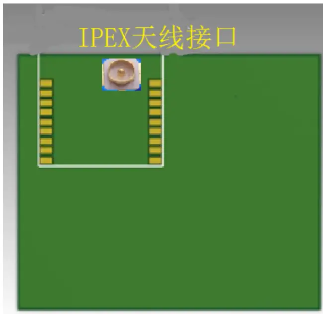
- Place the IPEX interface near the outline of the board.
- No shield should cover on the IPEX interface.
These suggestions are for the extend ANT interface pin used for IPEX ANT.
FPC Antenna
VWRK4 module can use an external IPEX antenna by the on board IPEX connector.
The FPC antenna is designed by Tuya cooperation,and manufacture by Dongguan UB electronic company.
The FPC Antenna is together with the VWRK4 module. if the costumer use their own new Antenna, the FCC should be tested with the new Antenna.
The following table is the main technical specifications of the FPC Antenna.
Items | Main technical specifications |
| Manufacturer | UB |
| Product model | UB01C07F3D1388A |
| Frequency Range (MHZ) | 2400~2500 |
| Impedance(Ω) | 50 |
| AVG Gain(dBi) | 2.13 |
| VSWR | ≤1.92 |
| Admitted Power | 1W |
| Polarization | Line |
| Connector Type | RF Cable+Terminal |
| Antenna Base | FPC |
| Operating Temp | -20℃~+70℃ |
| Storage Temp | -20℃~+70℃ |
The Figure 5-5 is the Picture of the FPC antenna. All the features of the FPC antenna can be reviewed from the “The Specification of the FPC antenna”.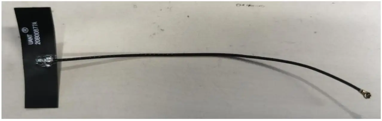
Figure 5-5 The FPC Antenna
Packaging Information
Mechanical Dimensions
The following is the mechanical dimensions of the VWRK4 module, the width and the length are 35mm*35mm.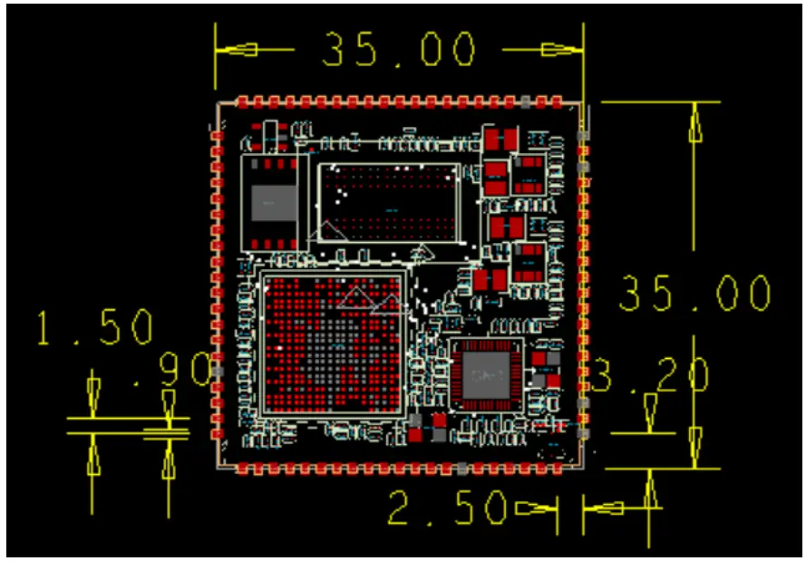
Figure 6-1 VWRK4 mechanical dimensions of top side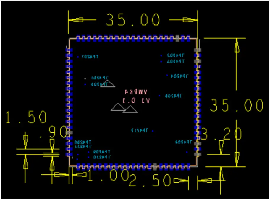
Figure 6-1 VWRK4 mechanical dimensions of bottom side
Note: The Pads beyond the dimensions are cutted and half left,if you want to design the package of the VWRK4, be careful of the pad dimensions.
Product instructions
Appendix: Statement
Federal Communications Commission (FCC) Declaration of Conformity
FCC Caution: Any changes or modifications not expressly approved by the party responsible for compliance could void the user’s authority to operate this equipment.
This device complies with Part 15 of the FCC Rules. Operation is subject to the following two conditions:
- This device may not cause harmful interference, and
- This device must accept any interference received, including interference that may cause undesired operation.
Note: This equipment has been tested and found to comply with the limits for a Class B digital device, pursuant to part 15 of the FCC Rules. These limits are designed to provide reasonable protection against harmful interference in a residential installation. This equipment generates, uses and can radiate radio frequency energy and, if not installed and used in accordance with the instructions, may cause harmful interference to radio communications. However, there is no guarantee that interference will not occur in a particular installation. If this equipment does cause harmful interference to radio or television reception, which can be determined by turning the equipment off and on, the user is encouraged to try to correct the interference by one or more of the following measures:
- Reorient or relocate the receiving antenna.
- Increase the separation between the equipment and receiver.
- Connect the equipment into an outlet on a circuit different from that to which the receiver is connected.
- Consult the dealer or an experienced radio/TV technician for help.
Radiation Exposure Statement
This equipment complies with FCC radiation exposure limits set forth for an uncontrolled rolled environment. This equipment should be installed and operated with minimum distance 20cm between the radiator and your body.
Important Note
This radio module must not installed to co-locate and operating simultaneously with other radios in host system except in accordance with FCC multi-transmitter product procedures. Additional testing and equipment authorization may be required to operating simultaneously with other radio.
The availability of some specific channels and/or operational frequency bands are country dependent and are firmware programmed at the factory to match the intended destination. The firmware setting is not accessible by the end user.
The host product manufacturer is responsible for compliance to any other FCC rules that apply to the host not covered by the modular transmitter grant of certification. The final host product still requires Part 15 Subpart B compliance testing with the modular transmitter installed.
The end user manual shall include all required regulatory information/warning as shown in this manual, including: This product must be installed and operated with a minimum distance of 20 cm between the radiator and user body.
This device have got a FCC ID: 2ANDL-VWRK4.The final end product must be labeled in a visible area with the following: “Contains Transmitter Module FCC ID:2ANDL-VWRK4”
This device is intended only for OEM integrators under the following conditions:
- The antenna must be installed such that 20cm is maintained between the antenna and users, and
- The transmitter module may not be co-located with any other transmitter or antenna.
As long as 2 conditions above are met, further transmitter test will not be required. However, the OEM integrator is still responsible for testing their end-product for any additional compliance requirements required with this module installed.
Declaration of Conformity European notice
 Hereby, Hangzhou Tuya Information Technology Co., Ltd declares that this module product is in compliance with essential requirements and other relevant provisions of Directive 2014/53/EU,2011/65/EU.A copy of the Declaration of conformity can be found at https://www.tuya.com
 This product must not be disposed of as normal household waste, in accordance with EU directive for waste electrical and electronic equipment (WEEE- 2012/19/EU). Instead,it should be disposed of by returning it to the point of sale, or to a municipal recycling collection point.
The device could be used with a separation distance of 20cm to the human body.


