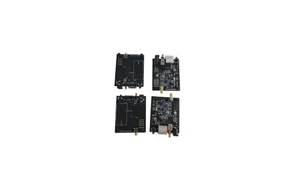
Lite On Technology WSG300NRC Wi-Fi HaLow 802.11ah Module User Manual
Overview
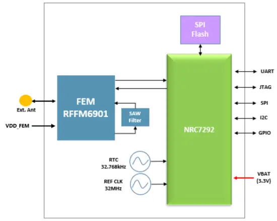
IEEE 802.11ah is a new Wi-Fi standard operating in the Sub 1GHz license-exempt band, offering longer range and lower power connectivity necessary for internet of things (IoT) applications. WSG300NRC contains external RF front end module (FEM) which can increase transmission power up to 23 dBm. Onboard serial flash can be used for OTA software development and with internal 32KB cache memory, it can support execution in place (XIP) feature.
Module features
The main features are represented as follows:
- Standard
- IEEE Std 802.11ahTM-2016 compliant
- 1/2/4 MHz channel bandwidth support
- WPA2 PSK support
- 150 kbps ~ 15 Mbps data rate
- AP and STA role support
- Radio frequency
- -109 dBm minimum receive sensitivity
- +23 dBm transmit power
- 920.5~924.5 MHz frequency band (By replacing RF SAW filter, other frequency band can be supported within 750~950 MHz)
- CPU
- ARM Cortex-M3 for application
- ARM Cortex-M0 for IEEE 802.11ah WLAN
- Clock frequencies for both processor (32/48 MHz)
- Host interface
- UART and SPI support for host interface
- Peripherals
- GPIO, ADC, PWM and timers
- I2C, SPI and UART
- Temperature range
- -40°C to +125°C
Applications
Low to high data rate can be applied in various IoT applications like:
- Wearable
- Home automation
- Healthcare
- Industrial automation
- Safety and security
- Smart grid
Multimedia streaming
Block Diagram
Pin Description
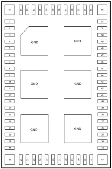
| Part no. | Name | Direction | Volt | Description |
| 1 | GROUND | GND | ||
| 2 | GROUND | GND | ||
| 3 | GROUND | GNO | ||
| 4 | GROUND | GND | ||
| 5 | VDD FEM | P | Module power input for FEM | |
| 6 | VBAT_33V | P | Module power input for SYS | |
| 7 | GROUND | GND | ||
| 8 | GROUND | GND | ||
| 9 | MODE 00 | I | SW define (When ROM BOOT) 11: Internal SRAM BOOT | |
| 10 | MODE 01 | I | ||
| 11 | MODE 02 | I | 0: ROM BOOT 1: )0P BOOT | |
| 12 | MODE 03 | I | 0: Cortex-MO Mater 1: Cortex-M3 Mater | |
| 13 | MODE 04 | I | 0: Two CPU 1: One CPU | |
| 14 | GROUND | GND | ||
| 15 | HSPl_nCS | I | Host SPI-Chip Select (active low) | |
| 16 | HSPI_CUC | I | Host SPI-Clock | |
| 17 | HSPI MISO | 0 | Host SPI-Mater in Slave out | |
| 18 | HSPI_MOSI | I | Host SPI-Mater out Slave in | |
| 19 | HSPI_EIRQ | 0 | Host SPI-Interrupt | |
| 20 | GROUND | GND | ||
| 21 | GROUND | GND | ||
| 22 | NC | – | ||
| 23 | NC | – | ||
| 24 | NC | – | ||
| 25 | GP 00 UART2 TX | I/O | UART Channel2 Tx | |
| 26 | GP 01 UART2_RX | I/O | UART Channel2 Rx | |
| 27 | GP 02 UART2_RTS | I/O | UNIT Channel2 RTS | |
| 28 | GP 03_UART2 CTS | I/O | UART Channel2 CTS | |
| 29 | GP 04 UARTO TX | I/O | UNIT Channel0 Tx | |
| 30 | GP 05_UARTO_RX | I/O | UNIT Channel0 Rx | |
| 31 | GP 06 UART3 TX | I/O | UART Channel3 Tx | |
| 32 | GP 07 UART3_RX | I/O | UNIT Channel3 Rx | |
| 33 | GP 08 UARTl_FIX | I/O | UART Channell Rx | |
| 34 | GP_11 UART1 TX | I/O | UART Channell Tx | |
| 35 | GP10 GPIO _ _ | I/O | Multiple purpose (GPIO, I2C, PWM, SPI, Ext-INT) | |
| 36 | GP 09 GPIO | I/O | ||
| 37 | GP_17 I2C SDA | I/O | I2C SDA | |
| 38 | GP 16 I2C SCL _ | I/O | I2C SCL | |
| 39 | GP_15_SSPO_CUC | 0 | SPIO Clock | |
| 40 | PD_14_SSPO_CS | 0 | SPIO Chip Enable (active low) | |
| 41 | PD_13_SSPO_MOSI | 0 | SPIO_Mater out Slave in | |
| 42 | PD_12_SSPO_MISO | I | SPIO_Mater in Slave out | |
| 43 | RESET | I | Reset (active high) | |
| 44 | GROUND | GND | ||
| 45 | JTAG TRSTN | I | JTAG reset | |
| 46 | HAG TMS | I | JTAG mode selection | |
| 47 | HAG Ta | I | JTAG dock | |
| 48 | JTAG TDI | 0 | JTAG data input | |
| 49 | JTAG TDO | I | JTAG data output | |
| 50 | GROUND | GND | ||
| 51 | VDDIO | P | Module I/0 supply input | |
| 52 | GROUND | GND | ||
| 53 | GROUND | GND | ||
| 54 | AUXADCIN3 | I | AUXADC input 3 | |
| 55 | AUXADCIN2 | I | AUXADC input 2 | |
| 56 | AUXADCIN1 | I | AUXADC input 1 | |
| 57 | GROUND | GND | ||
| 58 | NC | – | ||
| 59 | NC | – | ||
| 60 | GROUND | GND | ||
| 61 | GROUND | GND | ||
| 62 | RF ANT | I/O | RF IN/OUT | |
| 63 | GROUND | GND | ||
| 64 | GROUND | GND | ||
| 65 | GROUND | GND | ||
| 66 | GROUND | GND | ||
| 67 | GROUND | GND | ||
| 68 | GROUND | GND | ||
Absolute Maximum Rating
| Symbol | Rating | Min | Max | 1:nits |
| Storage Temperature | -40 | +125 | °C | |
| Supply Voltage | VBAT | -0.5 | 3.8 | V |
| VDDIO | -0.5 | 3.8 | V | |
NOTE: Stresses above those listed in Absolute Maximum Rating may cause permanent device failure. Functionality at or above these limits is not implied. Exposure to absolute maximum ratings for extended periods may affect device reliability.
Operating Condition
Operating condition
| Symbol | Rating | Min | Typ | Max | 1:nits |
| Operating Temperature Range | -40 | – | +85 | °C | |
| Operating Voltage | VBAT | 2.8 | 3.3 | 3.6 | V |
| VDDIO | 1.8 | 3.3 | VBAT | V | |
NOTE: To ensure WLAN performance, ripple on the 2.1- to 3.3-V supply must be less than ±300 mV and ripple on the 1.8-V supply must be less than 2% (±40 mV).
Current consumption
| Mode | i _ i i —)t.: Ilm L- | Band (MHz) | VBAT=3.3V, Ta=27°C |
| 802.11ah (1Mhz BW) | TX@18dBm | 9)2 | 200 |
| Continuous RX@-80dBm | 41 | ||
| 802.11ah (2Mhz BW) | TX@18dBm | 922 | 290 |
| Continuous RX@-80dBm | 41 | ||
| 802.11ah (4Mhz BW) | TX@18dBm | 922 | 200 |
| Continuous RX@-80dBm | 42 |
Note: Unless otherwise specified, TA=27°C, VBAT=3.6V, using internal PMU. Measurements are done at antenna port, which is directly connect to the device.
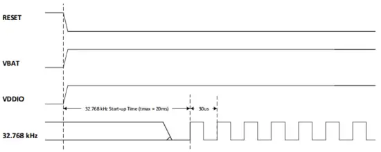
Power on sequence
AC Specifications
HSPI timing
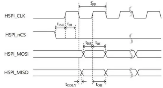
| Symbol | Parameter | Min | Typ | I Max | Unit |
| fpp | Frequency | – | – | 25 | MHz |
| tom | Output delay time | 6 | – | – | ns |
| to„ | Output hold time | 2 | – | – | ns |
| tisu | Input setup time | – | – | 14 | ns |
| Us | Input hold time | 3. | – | – | ns |
SPI Timing
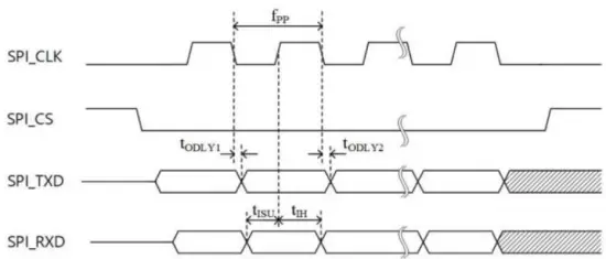
| Symbol | Parameter | Min | Typ | Max | Unit | ||
| fpp | Frequency | master | – | 24 | 24 | MHz | |
| slave | – | – | 4 | MHz | |||
| tort | Output delay time l | 0 | – | 10 | MHz | ||
| tOD1Y2 | Output delay time 2 | 0 | – | 10 | ns | ||
| tsu | Input setup time | 18 | – | – | ns | ||
| tu, | Input hold time | 20 | – | – | ns | ||
AUXADC Timing
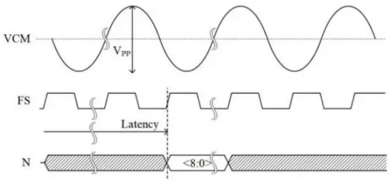
| Symbol | Parameter | Min | Typ | Max | Unit |
| VCM | Input common-mode voltage | 0.25 | 0.28 | 0.31 | V |
| Vpp | Input Swing | – | 0.5 | – | Vpp |
| FS | Sampling Clock | – | 32 | – | MHz |
| Latency | Conversion latency(1 cycle = 31.25 ns) | – | 11 | – | cycle |
| N | Resolution | – | 9 | – | Bit |
| RIN | Input impedance | – | 1 | – | Mohms |
| (_active | Current consumption (1.2V supply) | – | – | 300 | uA |
| !down | Power-down current (1.2V supply) | – | – | 1 | uA |
11ah WLAN RF Specifications and Performance
Transmitter Specifications
| Parameter | Conditions | Min | Typ | Max | Unit |
| RF Output Frequency Range in | 920.5 | 924.5 | MHz | ||
| 13.5 Mbps (MCS7, 4 MHz BW) | 18 | dBm | |||
| EVM compliant Output Power | |||||
| EVM at 0 dBm output power | 33 | dB | |||
| Transmitter Spurious Signal i Emissions | <700 MHz | <-36 | dBm/ | ||
| >1GHz | <45 | MHz | |||
| RF Output Return Loss | |||||
| Single ended output port | -10 | dB | |||
| Output 1dB Gain Compression | 0.4 MHz CW signal input | 25 | dBm | ||
| Gain Control Range | 30 | 30 | dB | ||
| Gain Control Step | 1 | dB | |||
| Unwanted Sideband | Over RF channel, RF frequency, and baseband frequency at 0 dBm output power | <-40 | dBc |
Note: Unless otherwise specified, TA=27°C, VBAT=3.6V, RF input/output specifications are referenced not device pins and do not include 1dB loss from EV kit OCB and SMA connector.
(1) RF output frequency range depends on RF SAW filter on the module. The NRC7292 chipset by itself can support frequency range from 750 to 950 MHz.
Receiver Specifications
| 1 Parameter | Conditions | Min | Typ | Max | Unit |
| RF Input Frequency Range “I | 921. | 925. | MHz | ||
| RF Input Return Loss | For LNA high/mid/low gain modes | -10 | -12 | -15 | dB |
| ‘ Total Voltage Gain Range | Analog + Digital Gain | -10 | 92 | dB | |
| RF Gain Step | From high gain mode to medium gain mode | 6 | dB | ||
| RX Gain Step | From RF to Analog | 1 | dB | ||
| DSB Noise Figure | LNA max gain mode | 4. | dB | ||
| IIP3 | LNA with high gain mode | -17 | dBm | ||
| LNA with low gain mode | 24 |
| Baseband Filters for Receiver ( log + Digital Filter) | |||||
| Baseband -3dB Low-pass Corner Frequency (Controllable) | 1 MHz channel | 0.5 | MHz | ||
| 2 MHz channel | 1.0 | MHz | |||
| 4 MHz channel | 2.0 | MHz | |||
Note: Unless otherwise specified, TA=27°C, VBAT=3.6V, RF input/output specifications are referenced not device pins and do not include 1dB loss from EV kit OCB and SMA connector. (1) RF output frequency range depends on RF SAW filter on the module. The NRC7292 chipset by itself can support frequency range from 750 to 950 MHz.
Transmitter Performance
| DR/MCS/BW bPs/ /MHz (hA ) | LEE Relative constellation error (dB) | EVM (%) (IEEE) | WM (%) (NRM7292A) | Comments |
| 0.15/MCS10/1 | -4 | 63. | 3. | BPSK Peak |
| 0.30/MCS0/1 | -5 | 56. | 3. | BPSK Peak |
| 0.60/MCS1/1 | -10 | 32. | 3. | 18 dBm OFDM, RMS |
| 0.90/MCS2/1 | -13 | 22. | 3. | 18 dBm OFDM, RMS |
| 1.20/MCS3/1 | -16 | 16. | 3. | 18 dBm OFDM, RMS |
| 1.80/MCS4/1 | -19 | 11. | 3. | 18 dBm OFDM, RMS |
| 2.40/MCS5/1 | -22 | 8. | 3. | 18 dBm OFDM, RMS |
| 2.70/MCS6/1 | -25 | 6. | 3. | 18 dBm OFDM, RMS |
| 3.00/MCS7/1 | -27 | 5. | 3. | 18 dBm OFDM, RMS |
| 0.65/MCS0/2 | -5 | 56. | 3. | BPSK Peak |
| 1.30/MCS1/2 | -10 | 32. | 3. | 18 dBm OFDM, RMS |
| 1.95/MCS2/2 | -13 | 22. | 3. | 18 dBm OFDM, RMS |
| 2.60/MCS3/2 | -16 | 16. | 3. | 18 dBm OFDM, RMS |
| 3.90/MCS4/2 | -19 | 11. | 3. | 18 dBm OFDM, RMS |
| 5.20/MCS5/2 | -22 | 8. | 3. | 18 dBm OFDM, RMS |
| 5.85/MCS6/2 | -25 | 6. | 3. | 18 dBm OFDM, RMS |
| 6.50/MCS7/2 | -27 | 5. | 3. | 18 dBm OFDM, RMS |
| 1.35/MCS0/4 | -5 | 56. | 3.0 | BPSK Peak |
| 2.70/MCS1/4 | -10 | 32. | 3.0 | 18 dBm OFDM, RMS |
| 4.05/MCS2/4 | -13 | 22. | 3.0 | 18 dBm OFDM, RMS |
| 5.40/MCS3/4 | -16 | 16. | 3.0 | 18 dBm OFDM, RMS |
| 8.10/MCS4/4 | -19 | 11. | 3.0 | 18 dBm OFDM, RMS |
| 10.80/MCS5/4 | -22 | 8. | 3.0 | 18 dBm OFDM, RMS |
| 12.15/MCS6/4 | -25 | 6. | 3.0 | 18 dBm OFDM, RMS |
| 13.50/MCS7/4 | -27 | 5. | 3.0 | _ 18 dBm OFDM, RMS |
Note: <Conditions> supply voltage VBAT 2.6-3.6V, TA=25°C, Signal within spectrum mask.
Receiver Performance
Receiver Sensitivity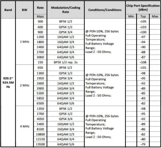
Adjacent Channel Rejection (ACR)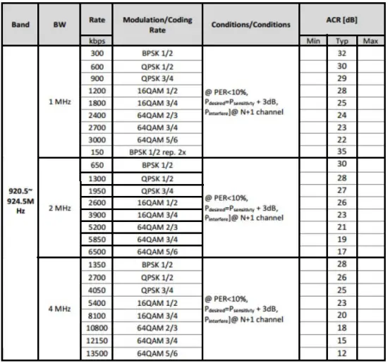
Product Characteristic
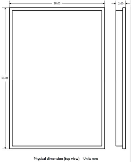
Product Dimension
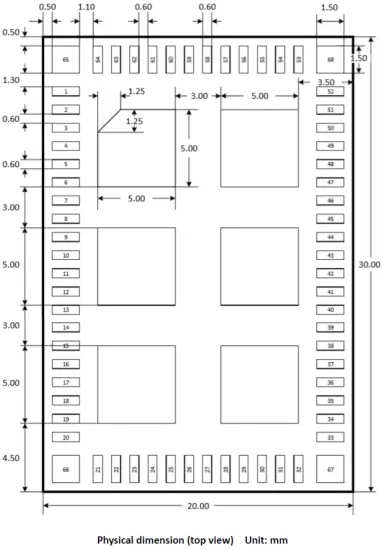
PAD Dimension
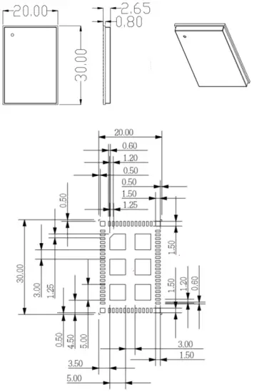
Recommend footprint
SMT Temperature Sequence (Pb-free)
Reflow profile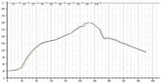
FCC Statement
Federal Communication Commission Interference Statement
This equipment has been tested and found to comply with the limits for a Class B digital device, pursuant to Part 15 of the FCC Rules. These limits are designed to provide reasonable protection against harmful interference in a residential installation. This equipment generates, uses and can radiate radio frequency energy and, if not installed and used in accordance with the instructions, may cause harmful interference to radio communications. However, there is no guarantee that interference will not occur in a particular installation. If this equipment does cause harmful interference to radio or television reception, which can be determined by turning the equipment off and on, the user is encouraged to try to correct the interference by one of the following measures:
- Reorient or relocate the receiving antenna.
- Increase the separation between the equipment and receiver.
- Connect the equipment into an outlet on a circuit different from that to which the receiver is connected.
- Consult the dealer or an experienced radio/TV technician for help.
FCC Caution: Any changes or modifications not expressly approved by the party responsible for compliance could void the user’s authority to operate this equipment.
This device complies with Part 15 of the FCC Rules. Operation is subject to the following two conditions: (1) This device may not cause harmful interference, and (2) this device must accept any interference received, including interference that may cause undesired operation. For product available in the USA/Canada market, only channel 1~11 can be operated. Selection of other channels is not possible. This device and its antenna(s) must not be co-located with any other transmitters except in accordance with FCC multi transmitter product procedures. Referring to the multi transmitter policy, multiple transmitter(s) and module(s) can be operated simultaneously without C2PC.
IMPORTANT NOTE: FCC Radiation Exposure Statement: This equipment complies with FCC radiation exposure limits set forth for an uncontrolled environment. This equipment should be installed and operated with minimum distance 20 cm between the radiator & your body.
IMPORTANT NOTE: This module is intended for OEM integrator. The OEM integrator is responsible for the compliance to all the rules that apply to the product into which this certified RF module is integrated. Additional testing and certification may be necessary when multiple modules are used.
20 cm minimum distance has to be able to be maintained between the antenna and the users for the host this module is integrated into. Under such configuration, the FCC radiation exposure limits set forth for an population/uncontrolled environment can be satisfied. Any changes or modifications not expressly approved by the manufacturer could void the user’s authority to operate this equipment.
USERS MANUAL OF THE END PRODUCT:
In the user’s manual of the end product, the end user has to be informed to keep at least 20 cm separation with the antenna while this end product is installed and operated. The end user has to be informed that the FCC radio frequency exposure guidelines for an uncontrolled environment can be satisfied. The end user has to also be informed that any changes or modifications not expressly approved by the manufacturer could void the user’s authority to operate this equipment. If the size of the end product is smaller than 8x10cm, then additional FCC part 15.19 statement is required to be available in the user’s manual: This device complies with Part 15 of FCC rules. Operation is subject to the following two conditions: (1) this device may not cause harmful interference and (2) this device must accept any interference received, including interference that may cause undesired operation.
LABEL OF THE END PRODUCT:
The final end product must be labeled in a visible area with the following ” Contains FCC ID: PPQ-WSG300NRC”. If the size of the end product is larger than 8x10cm, then the following FCC part 15.19 statement has to also be available on the label: This device complies with Part 15 of FCC rules. Operation is subject to the following two conditions: (1) this device may not cause harmful interference and (2) this device must accept any interference received, including interference that may cause undesired operation.
OEM Integrator Checklist
The party below will implement the LITE-ON Module in host systems in accordance with the instructions specified in this document and the documents referenced herein.
- The OEM integrator will ensure the Module is integrated in a host systems using only the approved antenna model(s) described in this document.
- The OEM integrator will ensure the antenna placement inside the host system will maintain the required spacing to end user for RF Exposure compliance, as specified in this document.
- If other radios are integrated inside the host with the LITE-ON Module, the OEM integrator will contact its test lab, TCB or LITE-ON to determine if additional FCC compliance evaluation is required to meet FCC collocation rules.
- The OEM integrator will ensure end user documentation will contain the specified regulatory wording and ensure the host system and the Module itself are labeled as specified in this document.
- The OEM integrator will ensure the Module is programmed in the factory with compliant transmit power not exceeding the levels specified in this document. LITE-ON requests that the OEM integrator acknowledge its receipt of this document and the above instructions. You may contact LITE-ON with any questions concerning this document or the responsibilities of the OEM integrator


