![]()
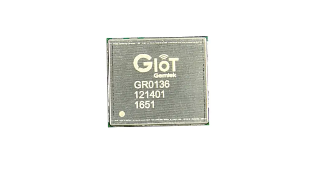
GR0136
RPMA Radio Communication
Module
Date: Nov. 30th, 2020
| Document Number | |
| Version | 0.6 |
| Created By | Steve Lin |
Modification History
| Date | Change log | Author | Revision |
| 09/03/2017 | First draft | Steve Lin | 0.1 |
| 13/04/2017 | Version Modified. | Steve Lin | 0.2 |
| 26/04/2017 | Version Modified. | Steve Lin | 0.3 |
| 15/11/2017 | Current consumption value revised. | Steve Lin | 0.4 |
| 08/11/2017 | Shield Cover Marking revised. | Steve Lin | 0.5 |
| 30/11/2020 | Adding FCC/IC/CE Regulatory Information. | Steve Lin | 0.6 |
General Description
The purpose of this document is to provide guidelines allowing an integrator to design a Host product that utilizes the GR0136 RPMA module and ensures that the system meets all of its technical objectives and requirements. The GR0136 RPMA module is a small form factor wireless network SiP module that easily integrates with various devices and sensors using an industry-standard Serial Peripheral Interface (SPI). The top side of the printed circuit board (PCB) is enclosed with a radio frequency (RF) shield. GR0136 RPMA module is an LGA-style module designed to be soldered directly onto a host board via SMT processes.
The RF technology operates on the Ingenu 2.4GHz RPMA two-way Communication Network. GR0136 can achieve a sensitivity of over -133 dBm. The high sensitivity combined with the integrated +21.5 dBm power amplifier yields industry leading link budget making it optimal for any low data rate application requiring range or robustness. RPMA also provides significant advantages in both blocking and selectivity over conventional modulation techniques, solving the traditional design compromise between range, interference immunity and energy consumption.
Features
- Small footprint 20.5 mm x 18 mm x 2.35 mm
- RPMA Modem
- +21.5 dBm constant RF output vs. V supply
- High sensitivity: down to -133 dBm
- Excellent blocking immunity
- Preamble detection
- Embedded memory of 1 Mbytes of Flash memory
1-1 Block Diagram
A simplified block diagram of the GR0136 RPMA module is depicted in the figure below.
PicoNode (GR0136) Block Diagram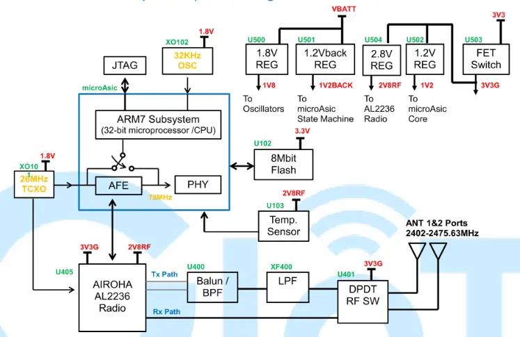
1-2 Product Version
The features of GR0136 is detailed in the following table
| Part Number | Frequency Range | Channel Bandwidth (M Hz) | Effective Bitrate (bps) | Est. Sensitivity ( dBm ) |
| GR0136 | 2.4 GHz | 1 | 60bps~30Kbps | -133 |
1-3 Specification
| Model Name | GR0136 |
| Product Description | RPMA Wireless Communication Module |
| Host Interface | SPI |
Operation Conditions | |
| Temperature | Storage:-40℃ ~ +85℃ Operating:-40℃ ~ +85℃ |
| Humidity | Operating:10 ~ 95% (Non-Condensing) Storage:5 ~ 95% (Non-Condensing) |
| Dimension | 20.5 mm x 18 mm x 2.35 mm |
| Package | LGA type |
Electrical Characteristic
2-1. Absolute Maximum Ratings
| Parameter | Min. | Max. | Unit |
| Storage Temperature | -40 | 85 | ⁰C |
| Operating Temperature | -40 | 85 | ⁰C |
| Vbatt Input Voltage | 2.2 | 6.0 | V |
| 3.3V Supply | 3.1 | 3.5 | V |
| Digital Interface Signals, 3.3V nominal | 3.0 | 3.6 | V |
2-2. Recommended Operating Range
Operating Conditions
| Parameter | Min. | Max. | Unit |
| Input voltage, VBATT | 2.2 | 5.5 | V |
| 3.3V Input | 3.2 | 3.4 | V |
| Ambient Temperature, Ta | -40 | 85 | ⁰C |
DC Characteristics
| Description | Min. | Typ. | Max. | Unit |
| Voltage – Vbatt | 2.2 | 3.3 | 5.5 | Volt |
| Off Current | 0.05 | 0.1 | 2.0 | µA |
| Deep Sleep Current | 19 | 30 | µA | |
| Idle Current | 20 | 26 | mA | |
| Receive Current | 105 | 120 | mA | |
| RPMA Node: Transmit Current (@21.5dBm) | 325 | 375 | mA |
Note: The above values with * mark in the DC Characteristics table are preliminary values.
Digital
| Description | Min. | Typ. | Max. | Unit |
| VOL – Voltage Output, Low (4mA sink) | 0 | 0.4 | V | |
| VOH – Voltage Output High (4mA source) | 2.4 | 3.3 | V | |
| SPI Clock – Note 11 | 0.1 | 8.6 | MHz |
Environmental
| Description | Min. | Typ. | Max. | Unit |
| Operating Temperature | -40 | +85 | °C | |
| Storage Temp | -40 | +85 | °C | |
| Humidity – non-condensing | 5 | 95 | % | |
| Ramp Temperature (the maximum rate at which operating temperature should change) | 30 | °C/Hr. | ||
| MTBF (RPMA Node) | TBD | MHrs |
Receiver
| Description | Min. | Typ. | Max. | Unit |
| Receiver Sensitivity | -130* | -133* | -135* | dBm |
| Noise Figure | 3.5 | 5 | 6.5 | dB |
| Maximum RF input level for specification compliance | -20* | dBm |
Note: The above values with * mark in Receiver table are preliminary values
General RF Characteristics
| Description | Min. | Typ. | Max. | Unit |
| Frequency Range | 2402 | ~2482 | MHz | |
| Channel Spacing | N/A | 1.99 | N/A | MHz |
Transmitter
| Description | Min. | Typ. | Max. | Unit |
| Maximum RF Conducted Power FCC/IC markets: | 21.5 | dBm | ||
| Signal Modulation | DSSS- DBPSK | |||
| Signal Bandwidth | 1.0 | MHz | ||
| BT Factor | 0.3 | |||
| Peak to Average Ratio | 2.3 | dB | ||
| Spectral bandwidth at maximum RF power: -6dB –20dB BW | 0.96 1.75 | MHz MHz | ||
| ACPR | -30 | dBc | ||
| Harmonics | -43 | dBm | ||
| Transmit Power Level Accuracy | ±1.5 | dB | ||
| Transmitter Spurious Outputs 30MHz to 2400MHz: 2482MHz to 8000MHz: | < -43 < -43 | dbm dbm | ||
| VSWR Tolerance Maximum VSWR for spec compliance maximum VSWR for stability. | 1.5:1 9:1 |
Pin Definition
3-1. Pin Assignment
| Pin | Definition | Signal Type | Description |
| 1 | GND | Power | Ground return |
| 2 | SRQ | Output | Slave Request |
| 3 | STURDY | Output | Slave Ready |
| 4 | SPI_MISO | Output | SPI Master Input Slave Output |
| 5 | SPI_CS0 | Input | SPI Chip Select |
| 6 | SPI_MOSI | Input | SPI Master Output Slave Input |
| 7 | SPI_SCLK | Input | SPI Clock |
| 8 | 3V3 | Power | The 3.3V can be continuously supplied or only when the WAKE pin is asserted “high”. This power domain is high power (internal CPU, Transceiver, and RF PA) and should be decoupled with a low ESR, high capacitance Capacitor. |
| 9 | TOUT | Output | TOUT is a normally low signal that pulses high in response to specific Network Timing Events. |
| 10 | TIME_QUAL | Output | This pin is used by the Extender for Node-based timing derivation. |
| 11 | GND | Power | Ground return |
| 12 | GND | Power | Ground return |
| 13 | GND | Power | Ground return |
| 14 | GND | Power | Ground return |
| 15 | GND | Power | Ground return |
| 16 | MRQ | Input | Master Request |
| 17 | RF_SHDN | RF Shutdown | This pin indicates the status of the RF Transceiver for GR0136 module: Low = Shutdown High = Active |
| 18 | ON_OFF | Input | This is used to turn ON/OFF the Internal Power supplies of the GR0136 module. Low: Node consumes <1uA High: Node is active and will run through a wide range of power states. |
| 19 | WAKE | Input | Wake up pin |
| 20 | VBATT | Power | Input power to GR0136 module. This power domain is low current but is used 100% of the time to supply Supervisory domains. |
| 21 | RF_TXENA | Output | This signal is used to indicate status of the Power Amplifier for the GR0136 module: Low = OFF High = Enabled (Transmitting) The rise edge can be used to trigger a Host CPU’s ADC read of VBATT (battery voltage while under maximum load). |
| 22 | GND | Power | Ground return |
| 23 | RF_PORT1 | 50 Ohm | RF port for GR0136 module. This is 50 Ohm port, DC coupled. RF1 is required but both are desired for antenna diversity. Single port or dual antenna port can be configured in the provisioning process. |
| 24 | GND | Power | Ground return |
| 25 | RF_PORT2 | 50 Ohm | RF port for GR0136 module. This is 50 Ohm port, DC coupled. Single port or dual antenna port can be configured in the provisioning |
| process. | |||
| 26 | GND | Power | Ground return |
| 27 | GND | Power | Ground return |
| 28 | GND | Power | Ground return |
| 29 | GND | Power | Ground return |
| 30 | GND | Power | Ground return |
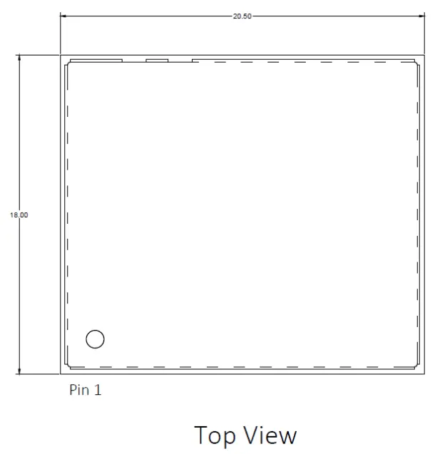
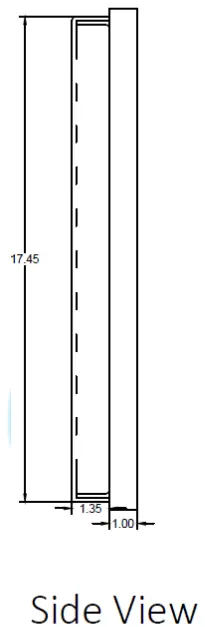
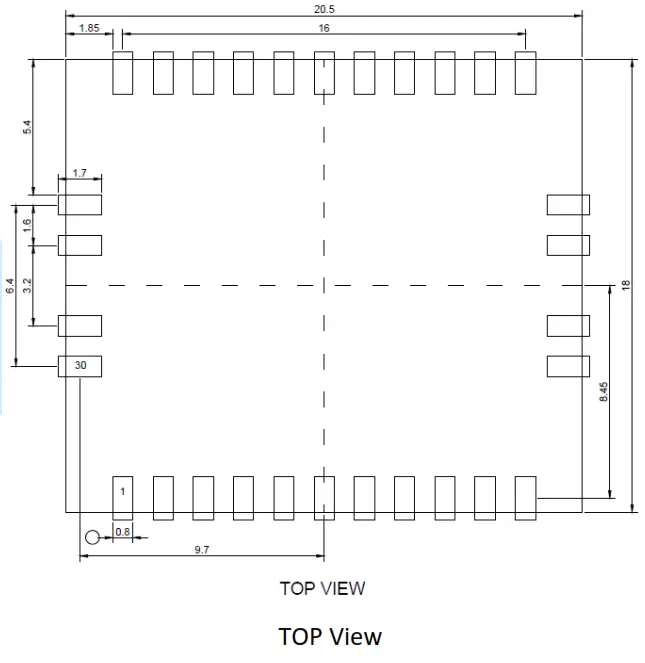
Mechanical Dimension
Unit: mm
 | 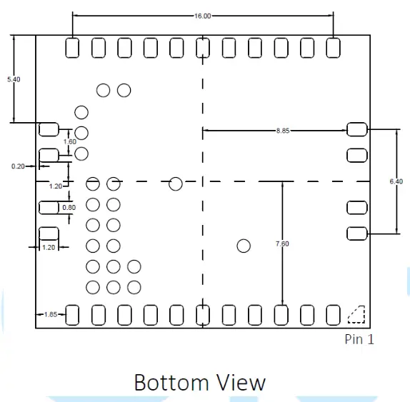 |  |
4-1 Recommended Footprint
Unit: mm
Recommended Reflow Profile
Reflow Profile for SiP on board Assembly
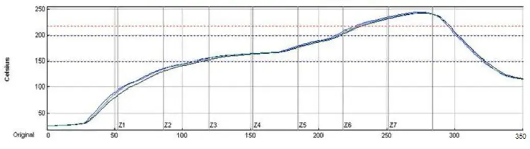
| Preheat time | -15sec 150°C 200°C: 105+1 |
| Dwell time | Over 220°C: 70+5/-10 sec |
| Peak Temp | 240 +10/-5°C |
| Ramp Up/Down Rate | Up: 3 +0/-2 °C/ sec Down: 2 +0/-1°C/ sec |
SiP Module Preparation
6-1. Handling
Handling the module must wear the anti-static wrist strap to avoid ESD damage. After each module is aligned and tested, it should be transported and stored with anti-static tray and packing. This protective package must remain in a suitable environment until the module is assembled and soldered onto the main board.
6-2. SMT Preparation
- Calculated shelf life in sealed bag: 6 months at<40 C and <90% relative humidity (RH).
- Peak package body temperature: 250 C.
- After the bag was opened, devices that will be subjected to reflow solder or another high-temperature process must.
A. Mounted within 168 hours of factory conditions<30’C/60%RH.
B. Stored at 10%RH with N2 flow box. - Devices require baking, before mounting, if:
A. Package bag does not keep in vacuumed while first time open.
B. Humidity Indicator Card is >10% when read at 23±5C.
C. Expose at 3A condition over 8 hours or Expose at 3B condition over 24 hours. - If baking is required, devices may be baked for 12 hours at 125±5 C .
Package Information
7.1 Product Making
Figure 1 below details the standard product marking for Gemtek GloT products. Cross-reference to the applicable line number and table for a full detail of all the variables.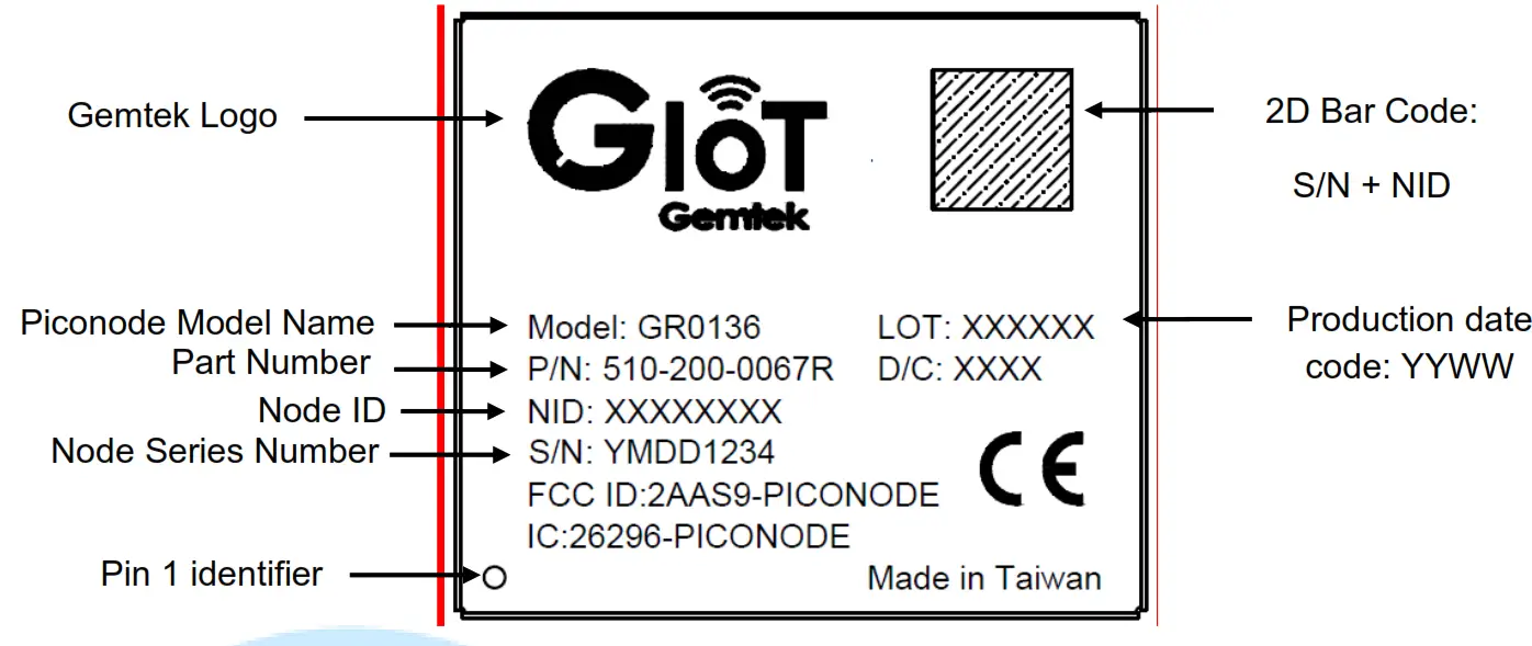
Figure 1 Standard Product Marking Diagram- TOP VIEW Scan result as below:
First line SN: 8 digit (HEX)
Second Line NID: 8 digit (HEX)
691D0001
00002372![]()
Regulatory Information
| Regulatory Region | Scope | Certificate ID |
| US | FCC | 2AAS9-PICO NODE |
| Canada | Industry Canada(IC) | 26296-PICO NODE |
| Europe | RED(Radio Equipment Directive) | No certificate ID since internal production control of A conformity assessment procedure is selected. |
GR0136 certification approvals
Integration instructions for host product manufacturers
Applicable FCC rules to module
FCC Part 15.247
Summarize the specific operational use conditions
The module is must be installed in the mobile device. This device is intended only for OEM integrators under the following conditions:
1) The antenna must be installed such that 20 cm is maintained between the antenna and users, and 2) The transmitter module may not be co-located with any other transmitter or antenna As long as 2 conditions above are met, further transmitter test will not be required. However, the OEM integrator is still responsible for testing their end-product for any additional compliance requirements required with this module installed.
IMPORTANT NOTE: In the event that these conditions can not be met (for example certain laptop configurations or co-location with another transmitter), then the FCC authorization is no longer considered valid and the FCC ID can not be used on the final product. In these circumstances, the OEM integrator will be responsible for re-evaluating the end product (including the transmitter) and obtaining a separate FCC authorization. The OEM integrator has to be aware not to provide information to the end-user regarding how to install or remove this RF module in the user’s manual of the end product which integrates this module.
The end-user manual shall include all required regulatory information gaming as shown in this manual.
Limited module procedures
Not applicable
Trace antenna designs
See the documents: “GR0136_Antenna_2020_1130” & “Test Procedure of embedded Antenna for GR0136 GIOT module”
RF exposure considerations
20 cm separation distance and co-located issue shall be met as mentioned in “Summarize the specific operational use conditions”. The product manufacturer shall provide the below text in the end-product manual “This equipment complies with FCC radiation exposure limits set forth for an uncontrolled environment. This equipment should be installed and operated with a minimum distance 20cm between the radiator & your body.”
Antennas
| Brand name | Model name | Antenna type | Antenna gain | Antenna connector |
| Linx | ANT-2.4-USP | Mono-pole | 3.8 (dBi) | RSMA |
| Taiyo Yuden | AH 104F2450S1 | Mono-pole (Inverted F) | 1.9 (dBi) | RSMA |
| Taoglas | GW.34.5153 | Dipole | 5.89 (dBi) | RSMA |
| Ethertronics | 1001013 | PIFA / magnetic Dipole | 2.6 (dBi) | — |
| Jesoncom | 10I010D | Mono-pole | 4.8 (dBi) | RSMA |
Label and Compliance Information
Product manufacturers need to provide a physical or e-label stating
“Contains FCC ID: 2AAS9-PICONODE” with the finished product
Information on Test Modes and Additional Testing Requirements
EMC Certification Tools, Version: 1.6.14.1shall be used to set the module to transmit continuously.
Additional Testing, Part 15 Subpart B Disclaimer
The module is only FCC authorized for the specific rule parts listed on the grant, and the host product manufacturer is responsible for compliance to any other FCC rules that apply to the host not covered by the modular transmitter grant of certification. The final host product still requires Part 15 Subpart B compliance testing with the modular transmitter installed.
Industry Canada statement
This device contains license-exempt transmitter(s)/receiver(s) that comply with Innovation, Science and Economic Development Canada’s license-exempt RSS(s). Operation is subject to the following two conditions:
(1) This device may not cause interference (2) This device must accept any interference, including interference that may cause undesired operation of the device
This radio transmitter [IC: 26296-PICONODE] has been approved by Innovation, Science and Economic Development Canada to operate with the antenna types listed below, with the maximum permissible gain indicated. Antenna types not included in this list that have a gain greater than the maximum gain indicated for any type listed are strictly prohibited for use with this device.
| Brand name | Model name | Antenna type | Antenna gain | Antenna connector |
| Linx | ANT-2.4-USP | Mono-pole | 3.8 (dBi) | RSMA |
| Taiyo Yuden | AH 104F2450S1 | Mono-pole (Inverted F) | 1.9 (dBi) | RSMA |
| Taoglas | GW.34.5153 | Dipole | 5.89(dBi) | RSMA |
| ethertronics | 1001013 | PIFA / magnetic Dipole | 2.6 (dBi) | — |
| Jesoncom | 10I010D | Mono-pole | 4.8 (dBi) | RSMA |
Radiation Exposure Statement:
This equipment complies with Canadian radiation exposure limits set forth for an uncontrolled environment. This equipment should be installed and operated with a minimum distance 20cm between the radiator & your body.
This device is intended only for OEM integrators under the following conditions: 1) The transmitter module may not be co-located with any other transmitter or antenna. As long as 1 condition above are met, further transmitter test will not be required. However, the OEM integrator is still responsible for testing their end-product for any additional compliance requirements required with this module installed.
IMPORTANT NOTE:
In the event that these conditions can not be met (for example certain laptop configurations or co-location with another transmitter), then the Canada authorization is no longer considered valid and the IC ID can not be used on the final product. In these circumstances, the OEM integrator will be responsible for re-evaluating the end product (including the transmitter) and obtaining a separate Canada authorization.
End Product Labeling
The final end product must be labeled in a visible area with the following: “Contains IC:26296- PICONODE”.
Manual Information To the End-User
The OEM integrator has to be aware not to provide information to the end-user regarding how to install or remove this RF module in the user’s manual of the end product which integrates this module.
The end-user manual shall include all required regulatory information/warning as show in this manual.


