HOPERF RFM380F32 434MHz SoC Wireless Transceiver Module
434MHz SoC Wireless transceiver module
Product overview
The RFM380F64 is an integrated ARM Cortex-M0 32-bit CPU kernel with an ultra-low-powerRFtransceiver,low-powerconsumption,highsensitivity,remote communication, and a highly cost-effective SoC RF transceiver module. Integrated with rich peripherals, support standard UART, I2C and SPI interfaces, providing multiple general IO, support internal fast RC concussion, internal slow RC concussion and 32.768 kHz external crystal oscillator, support multiple package formats and codec, up to 64-byte Tx / Rx FIFO, feature-rich RF GPIO, multiple low-power operating modes and fast start mechanism, high precision RSSI, manual fast frequency hopping and multi-channel input 12-bit high-speed ADC. The product is divided into 434MHz working frequencies, supporting a data rate range of 0.5-300kbps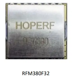
product features
- Super anti-interference ability, suitable for the use of complex interference environment scenarios
- Receive sensitivity: -120 d B m @ 434MHz,0.6bps, GFSK
- Operating frequency: 434MHz
- Power supply voltage input range: 1.8V—3.6V
- Emission current: 74mA @ + 20dBm, 434MHz
- Receive current: 12mA @434MHz, FSK
- Deep sleep current: 2.5uA
- Operating rate: 0.5-300 kbps
applied range
- Automatic meter reading
- Furniture Security and Building automation
- Wireless sensing nodes and industrial monitoring
- ISM frequency band data communication
Product foot position
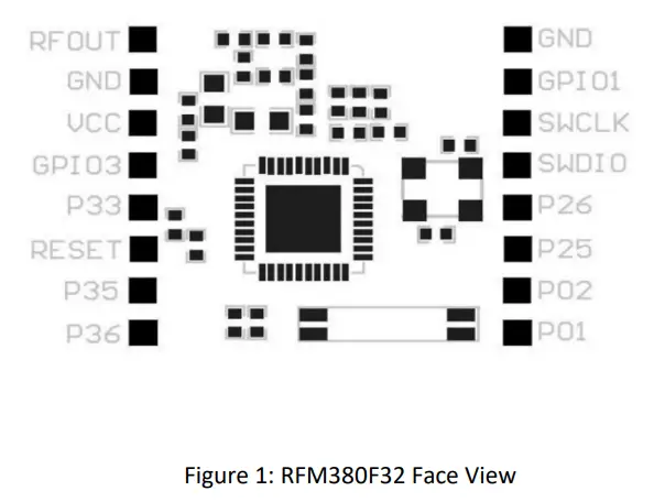
Table 1, the foot-bit definition of the RFM380F32
| foot | name | describe | Configuration function |
| 1 | P36 | MCU and so on IO | UART1_RXD、TIM6_CHA、UART0_RXD、PCA_CH4、TIM5_CHA、 spi_mosi、i2c_scl、AIN6/VC6/AVREF |
| 2 | P35 | MCU and so on IO | UART0_TXD,TIM0_GATE、TIM4_CHB、SPI_MISO,I2C_SDA, AIN5/VC5,UART1 TXD |
| 3 | RESET | Hard reset pin | ——————- |
| 4 | P33 | MCU and so on IO | UART2_RXD、pca_ch1、tim5_chb、PCA_ECI、UART1_RXD、 XTL_OUT、TIM1_TOGN、AIN3/VC3 |
| 5 | GPIO3 | The GPIO3 of the RF | CLKO, DOUT/DIN, INT2,DCLK (TX/RX) |
| 6 | VCC | Positive power supply | ——————— |
| 7 | GND | earth wire | ——————– |
| 8 | RFOUT | RF output | ——————— |
| 9 | P01 | MCU and so on IO | UART0_RXD,I2C_SDA, UART1_TXD, TIM0_TOG, TIM5_CHB, SPI_SCK, TIM2_EXT, AIN7/VC7,XTHI |
| 10 | P02 | MCU and so on IO | uart0_txd,i2c_scl,uart1_rxd,tim0_togn,tim6_cha,spi_cs, tim2_gate,ain8,extho |
| 11 | P25 | MCU and so on IO | SPI_SCK、pca_ch0 、tim5_cha、LVD_OUT、UART2_RXD、 I2C_SDA、TIM1_GATE、LVDIN3/VC1 |
| 12 | P26 | MCU and so on IO | SPI_MOSI,TIM4_CHA,TIM5_CHB,PCA_CH2,UART2_TXD, I2C_SCL,TIM1_EXT,AIN |
| 13 | SWDIO | SW shakedown test IO | —— |
| 14 | SWCLK | TheSW debugging clock | ——– |
| 15 | GPIO1 | The GPIO1 of the RF | DOUT/DIN, INT1,INT2,DCLK (TX/RX),RF_SWT |
remarks:
- RFM380F32 chip 32nd foot SCLK and chip 27th foot has been external connected
- RFM380F32 chip 33rd foot SDA and the chip 26th foot are external connected
- RFM380F32 chip 34th foot CSB and the chip 23th foot are external connected
- RFM380F32 chip 35th foot FCSB and chip 9th foot has been external
Electrical parameters
Test conditions, power supply 3.3V, temperature 25℃
Table 2, a list of electrical parameters
| parameter | symbol | status | least value | representa tive value | crest value | unit |
| service frequency | RFM380F32-433S2 | 434 | MHZ | |||
| mode | MOD | FSK | ||||
| receiving sensitivity | 434MHz1 Kbps | -120 | DBM | |||
| data rate | DR | 0.5 | 2.4 | 300 | Kbps | |
| Receive bandwidth | BW | 50 | 330 | KHZ | ||
| working voltage | VDD | 1.8 | 3.3 | 3.6 | V | |
| Receiveworking current | IRX | 434MHZ | 9 | 10 | mA | |
| Launchworking current | ITX | 434MHZ +20dbm | 70 | 80 | mA | |
| Sleep current | ISleep | 1 | uA | |||
| image rejection | IMR | 33 | dB | |||
| image rejection | Top | -40 | +80 | ℃ |
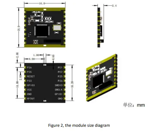
Module outline dimension drawing
FCC Statement
FCC standards: FCC CFR Title 47 Part 15 Subpart C Section 15.231
Trace antenna with antenna gain 3.555dBi
This device complies with part 15 of the FCC Rules. Operation is subject to the following two conditions: (1) This device may not cause harmful interference, and (2) this device must accept any interference received, including interference that may cause undesired operation.
Any Changes or modifications not expressly approved by the party responsible for compliance could void the user’s authority to operate the equipment.
Note: This equipment has been tested and found to comply with the limits for a Class B digital device, pursuant to part 15 of the FCC Rules. These limits are designed to provide reasonable protection against harmful interference in a residential installation. This equipment generates, uses and can radiate radio frequency energy and, if not installed and used in accordance with the instructions, may cause harmful interference to radio communications. However, there is no guarantee that interference will not occur in a particular installation. If this equipment does cause harmful interference to radio or television reception, which can be determined by turning the equipment off and on, the user is encouraged to try to correct the interference by one or more of the following measures:
- Reorient or relocate the receiving antenna.
- Increase the separation between the equipment and receiver.
- Connect the equipment into an outlet on a circuit different from that to which the receiver is connected.
- Consult the dealer or an experienced radio/TV technician for help.
FCC Radiation Exposure Statement
This modular complies with FCC RF radiation exposure limits set forth for an uncontrolled environment. This transmitter must not be co-located or operating in conjunction with any other antenna or transmitter. If the FCC identification number is not visible when the module is installed inside another device, then the outside of the device into which the module is installed must also display a label referring to the enclosed module. This exterior label can use wording such as the following: “Contains Transmitter Module FCC ID: 2ASEORFM380F32 Or Contains FCC ID: 2ASEORFM380F32”
When the module is installed inside another device, the user manual of the host must contain below warning statements;
- This device complies with Part 15 of the FCC Rules. Operation is subject to the following two conditions:
- This device may not cause harmful interference.
- This device must accept any interference received, including interference that may cause undesire operation.
Note: This equipment has been tested and found to comply with the limits for a Class B digital device, pursuant to part 15 of the FCC Rules. These limits are designed to provide reasonable protection against harmful interference in a residential installation. This equipment generates, uses and can radiate radio frequency energy and, if not installed and used in accordance with the instructions, may cause harmful interference to radio communications. However, there is no guarantee that interference will not occur in a particular installation. If this equipment does cause harmful interference to radio or television reception, which can be determined by turning the equipment off and on, the user is encouraged to try to correct the interference by one or more of the following measures:- Reorient or relocate the receiving antenna.
- Increase the separation between the equipment and receiver.
- Connect the equipment into an outlet on a circuit different from that to which the receiver is connected.
- Consult the dealer or an experienced radio/TV technician for help.
- Changes or modifications not expressly approved by the party responsible for compliance could void the user’s authority to operate the equipment.
The devices must be installed and used in strict accordance with the manufacturer’s instructions as described in the user documentation that comes with the product. Any company of the host device which install this modular with modular approval should perform the test of radiated & conducted emission and spurious emission,etc. according to FCC part 15C : 15.231 and 15.209 & 15.207 ,15B Class B requirement, Only if the test result comply with FCC part 15C : 15.231 and 15.209 & 15.207 ,15B Class B requirement,then the host can be sold legally.
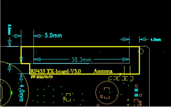
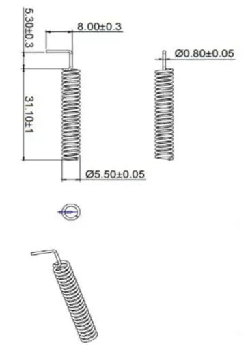
- Directional spring antenna specification
- Below is ntenna specification
- You can see antenna size from below specification
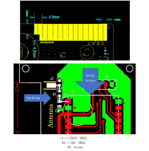
 And PCB Pad size for spring antenna just follow the below chart.
  Spring antenna location on PCB are J2, and the Empty Area except spring antenna should be see just follow the below two charts.

 And PCB Pad size for spring antenna just follow the below chart.
 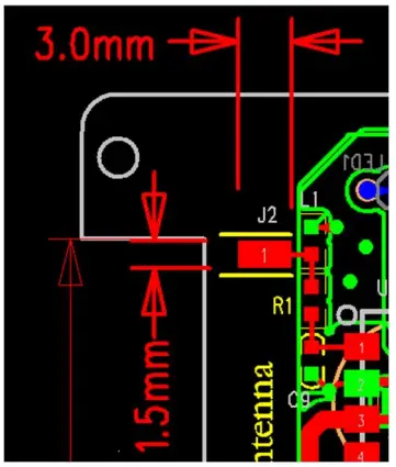 Spring antenna location on PCB are J2, and the Empty Area except spring antenna should be see just follow the below two charts.