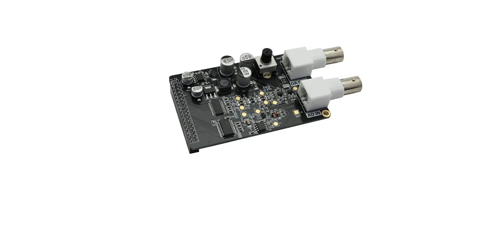
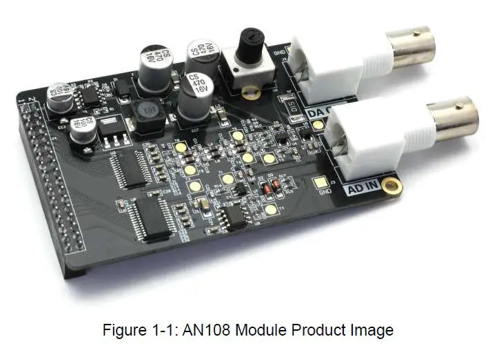
ALINX AN108 High-Speed AD-DA Module
Product Information
The High-Speed AD/DA Module AN108 is a module that allows for high-speed analog-to-digital and digital-to-analog conversion. The module has a 34-pin standard interface and consists of a high-speed DA chip (AD9708), a 7th order Butterworth low pass filter, an amplitude adjustment circuit, a signal output interface (10Vpp), a high-speed AD chip (AD9280), an attenuation circuit (attenuation to 0-2V).
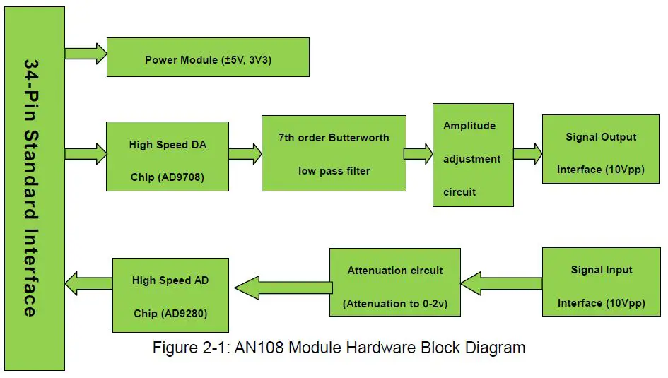
Hardware Block Diagram
The hardware block diagram of the module is shown in Figure 2-1 of the user manual. The signal input interface and signal output interface have a range of 10Vpp. The DA circuit consists of a high-speed DA chip, a 7th-order Butterworth low-pass filter, an amplitude adjustment circuit, and a signal output interface. The AD circuit consists of a high-speed AD chip, an attenuation circuit, and a signal input interface.
Digital to Analog Conversion Circuit
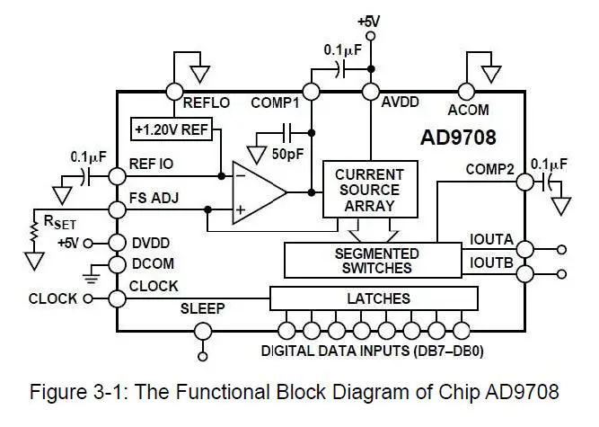
The DA circuit uses the AD9708 chip, an 8-bit, 125MSPS DA conversion chip with a built-in 1.2V reference and differential current output. After the differential output of the AD9708 chip, a 7th-order Butterworth low-pass filter is connected to the circuit with a bandwidth of 40MHz to prevent noise interference. The frequency response is shown in Figure 3-2 of the user manual. Two high-performance 145MHz bandwidth op amp AD8056 are used to achieve differential conversion to single-ended, amplitude adjustment, and other functions. The amplitude is adjusted using a 5K potentiometer and the final output range is -5V to 5V (10Vpp).
Analog to Digital Conversion Circuit
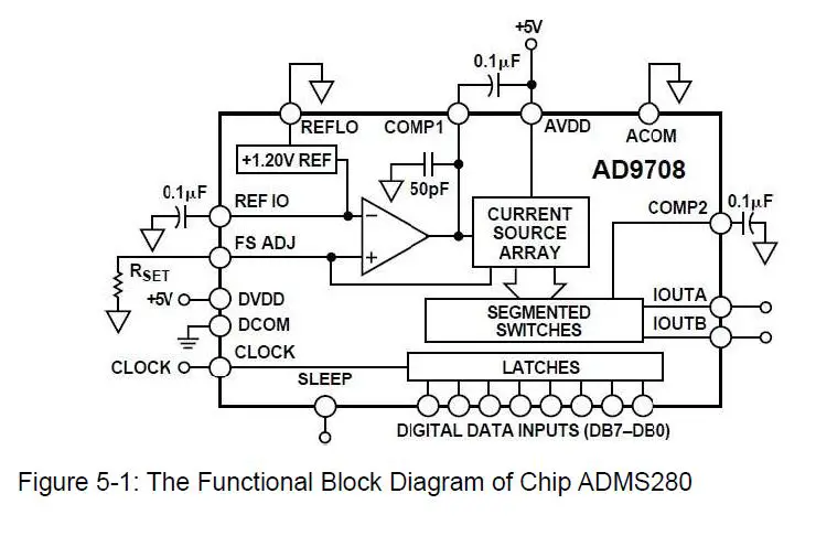
The AD circuit uses the ADMS280 chip, an 8-bit, maximum sampling rate of 32MSPS, AD chip. The input range of the interface is -5V~+5V (10Vpp). Before the signal enters the AD chip, an attenuation circuit is constructed with a piece of the AD8056 chip. The input range of the interface is -5V~+5V (10Vpp). After attenuation, the input range meets the input range of the AD chip (0~2V).
Product Usage Instructions
To use the High-Speed AD/DA Module AN108, follow the steps below:
- Connect the module to the device using the 34-pin standard interface.
- For analog-to-digital conversion, connect the signal source to the signal input interface with a range of 10Vpp. If necessary, use the attenuation circuit to adjust the input range to -5V~+5V (10Vpp) to match the input range of the AD chip.
- For digital-to-analog conversion, connect the signal output interface with a range of 10Vpp to the output device. Adjust the amplitude using the 5K potentiometer if necessary.
High-Speed AD/DA Module AN108
Hardware Block Diagram
Digital to Analog Conversion Circuit
- As shown in Figure 2-1 the hardware block diagram, the DA circuit consists of a high-speed DA chip, a 7th-order Butterworth low-pass filter, an amplitude adjustment circuit, and a signal output interface.
- The high-speed DA chip we use is the AD9708 from AD. The AD9708 is an 8-bit, 125MSPS DA conversion chip with a built-in 1.2V reference and differential current output. Figure 3-1 is the functional block diagram of chip AD9708.
- After the differential output of the AD9708 chip, in order to prevent noise interference, a 7th-order Butterworth low-pass filter is connected to the circuit with a bandwidth of 40MHz. The frequency response is shown in Figure 3-2 below:
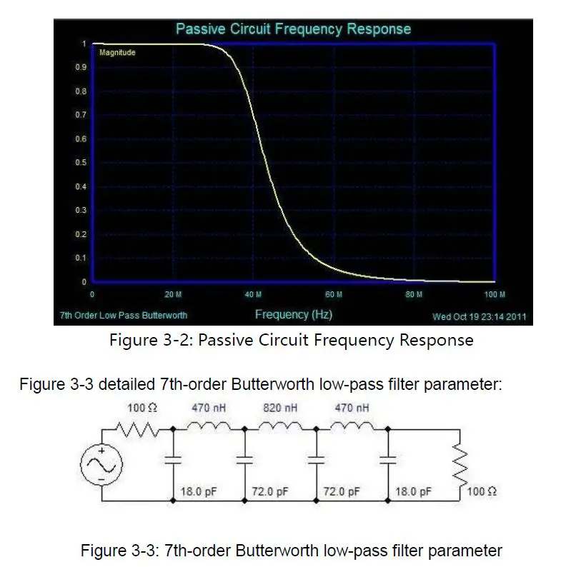
After the filter, we used two high-performance 145MHz bandwidth op amp AD8056 to achieve differential conversion to single-ended, amplitude adjustment, and other functions, so that the overall circuit performance has been maximized. The amplitude is adjusted using a 5K potentiometer and the final output range is -5V to 5V (10Vpp).
Note: Since the accuracy of the potentiometer is not very accurate, the final output has a certain error. It is possible that the waveform amplitude cannot reach 10Vpp, and there may be problems such as waveform clipping. These are normal conditions.
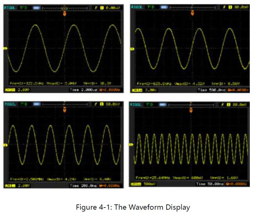
Waveform Display
Analog to Digital Conversion Circuit
- As shown in Figure 2-1 the hardware block diagram, the AD circuit consists of a high-speed AD chip, an attenuation circuit, and a signal input interface.
- The high-speed AD chip used in the high-speed AD/DA module AN108 is an 8-bit, maximum sampling rate of 32MSPS, ADMS280 chip of AD. Figure 5-1 is the functional block diagram of chip ADMS280.
- According to the configuration shown in Figure 5-2 below, we set the AD voltage input range to: 0V~2V.
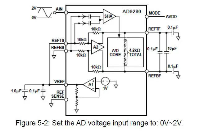
- Before the signal enters the AD chip, an attenuation circuit is constructed with a piece of the AD8056 chip. The input range of the interface is -5V~+5V (10Vpp). After attenuation, the input range meets the input range of the AD chip (0~2V). The conversion formula is as follows:
- When the input signal Vin=5(V), the signal input to AD Vad=2(V); When the input signal Vin=-5(V), the signal input to AD Vad=0(V);
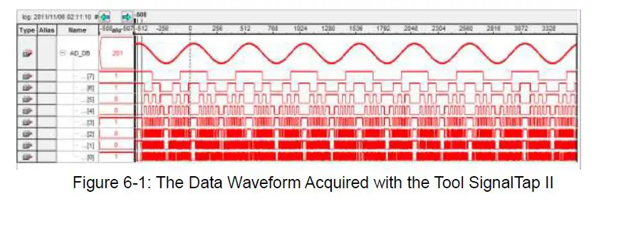
SignalTap II Waveform
- The waveform in Figure 6-1 below is the data waveform acquired with the tool SignalTap II in the Quartus II software.
Interface definition
(J4 in the schematic diagram, the square pin the PCB labeled is pin 1)
| Pin | Pin Name | Description | Pin | Pin Name | Description |
| 1 | DCOM | Ground | 2 | VCC | +5V |
| 3 | 4 | ||||
| 5 | DACLK | DA Clock Line | 6 | DADB7 | DA Data Line |
| 7 | DADB6 | DA Data Line | 8 | DADB5 | DA Data Line |
| 9 | DADB4 | DA Data Line | 10 | DADB3 | DA Data Line |
| 11 | DADB2 | DA Data Line | 12 | DADB1 | DA Data Line |
| 13 | DADB0 | DA Data Line | 14 | ||
| 15 | 16 |
| 17 | 18 | ||||
| 19 | 20 | ||||
| 21 | ADDB0 | AD Data Line | 22 | ADDB1 | AD Data Line |
| 23 | ADDB2 | AD Data Line | 24 | ADDB3 | AD Data Line |
| 25 | ADDB4 | AD Data Line | 26 | ADDB5 | AD Data Line |
| 27 | ADDB6 | AD Data Line | 28 | ADDB7 | AD Data Line |
| 29 | ADCLK | AD Clock Line | 30 | ||
| 31 | 32 | ||||
| 33 | 34 |
DA Experiment Steps
- First, connect the high-speed AD/DA module AN108 to the 34-pin standard expansion port of the ALINX series FPGA development board. (in case of power off).
- When doing DA experiments, you need an oscilloscope to match the AD output port (near potentiometer BNC interface J2) is connected to the oscilloscope interface via the cable provided.
- Download the program to the FPGA using the Quartus II software (the test program provided).
- Adjust the oscilloscope to display the full waveform correctly.
- Manually adjust the amplitude of the waveform with a potentiometer (U6).
AD Experiment Steps
- First, connect the high-speed AD/DA module AN108 to the 34-pin standard expansion port of the ALINX series FPGA development board. (in case of power off).
- This experiment requires the cooperation of the DA experiment, which means that we need to pass the DA output signal to the AD input port. Of course, if you have a signal source, it is better. Use the cable provided to connect the output interface of the signal source to the AD input interface (J3) (Note: AD port input range: -5V~+5V).
- Download the program to the FPGA using the Quartus II software (the test program provided).
- Real-time data collection with SignalTap II.


